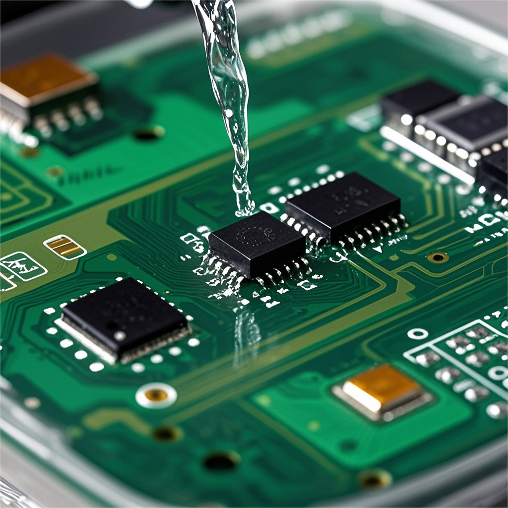
Why is copper used in PCBs? Because of its strong electrical conductivity, it can ensure efficient signal transmission; excellent thermal conductivity, can quickly dissipate heat; stable chemical properties, can resist corrosion to ensure reliable circuits; good processability, meet the needs of PCB miniaturization; and good cost-effectiveness and compatibility, it is an ideal choice for PCB manufacturing.
What material is commonly used for PCBs?
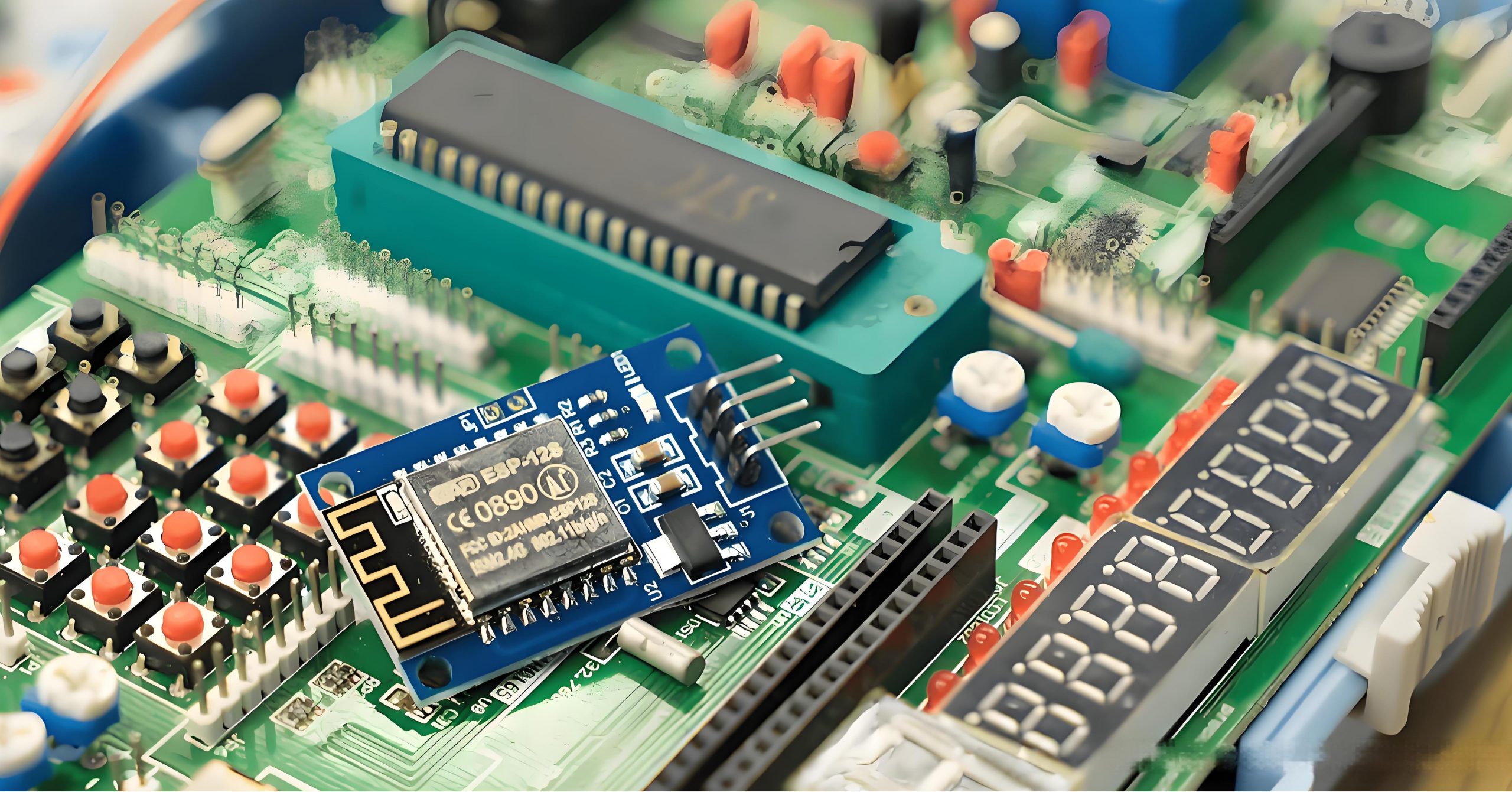
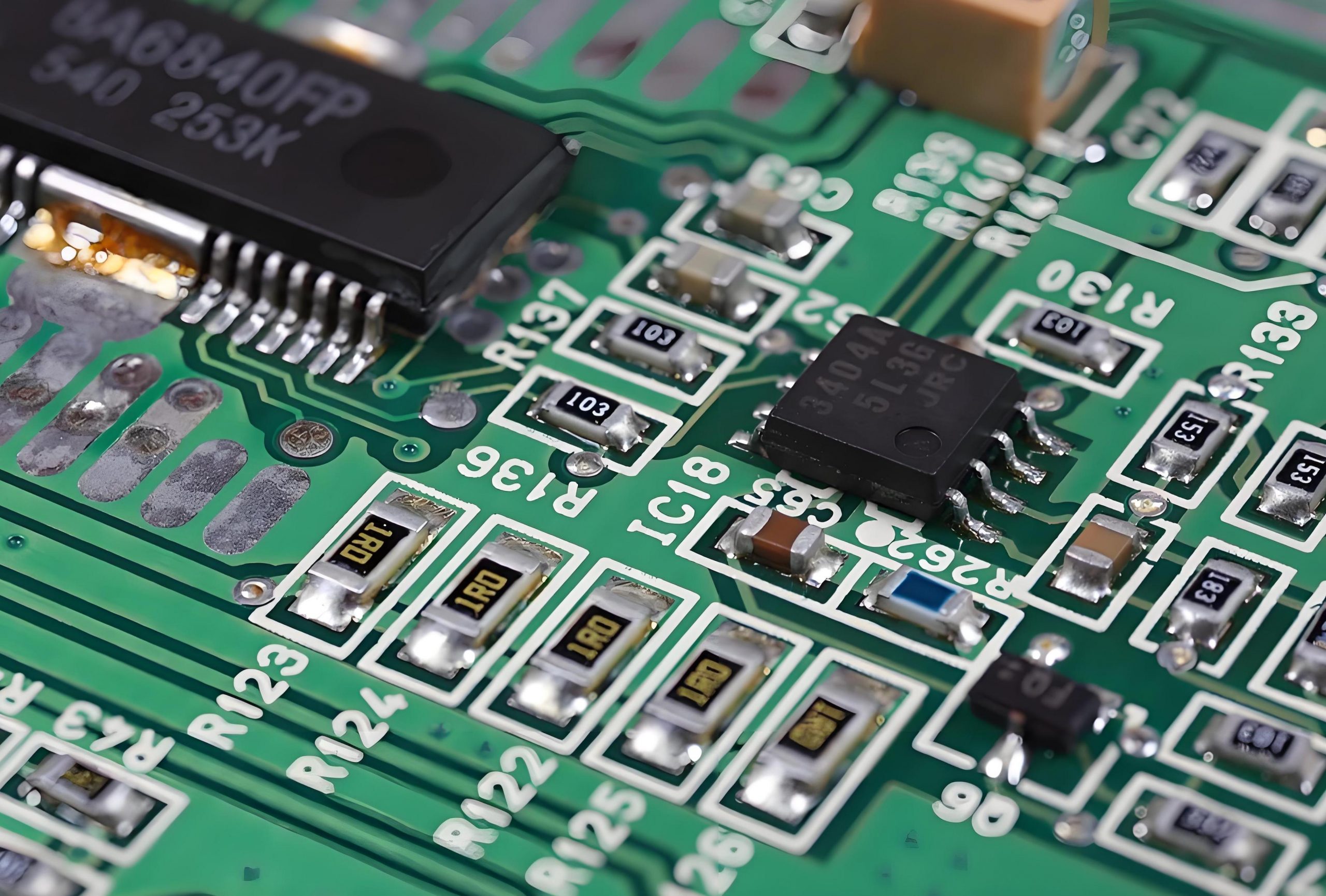
The materials commonly used for PCBs include FR-4, metal substrates, ceramic substrates, polymer materials, etc. These materials have their own characteristics and are suitable for different application scenarios.
- 1. FR-4
FR-4 is a glass fiber reinforced plastic and is the most commonly used substrate in the PCB manufacturing process. It has excellent electrical properties, mechanical properties, thermal properties and weather resistance, and is widely used in home appliances, office electronic equipment, automotive electronics, industrial controllers and other fields.
- 2. Metal substrate
A metal substrate is a PCB board with a metal film plated on the substrate. Commonly used metals include aluminum, copper, iron, nickel, stainless steel, etc. It has excellent heat dissipation and shock resistance, and is suitable for high-power electronic equipment, LED lighting, automotive electronics and other fields. But metal substrates are expensive and have high manufacturing costs.
- 3. Ceramic substrates
Ceramic substrates are very hard, high-temperature-resistant and corrosion-resistant materials, usually made of high-purity alumina or silicon nitride. They are suitable for high-frequency, high-power and high-precision electronic components, and are mainly used in high-end fields such as military industry, aerospace, and medical treatment.
- 4. Polymer materials
Polymer materials include polyimide, acrylic, polyamide and epoxy resin, which have good mechanical properties, dimensional stability and thermal stability, and are suitable for high-density, high-speed and high-precision circuit boards. They are mainly used in semiconductor production equipment, optical instruments, aerospace, military industry and other fields.
What is the core material of a PCB?
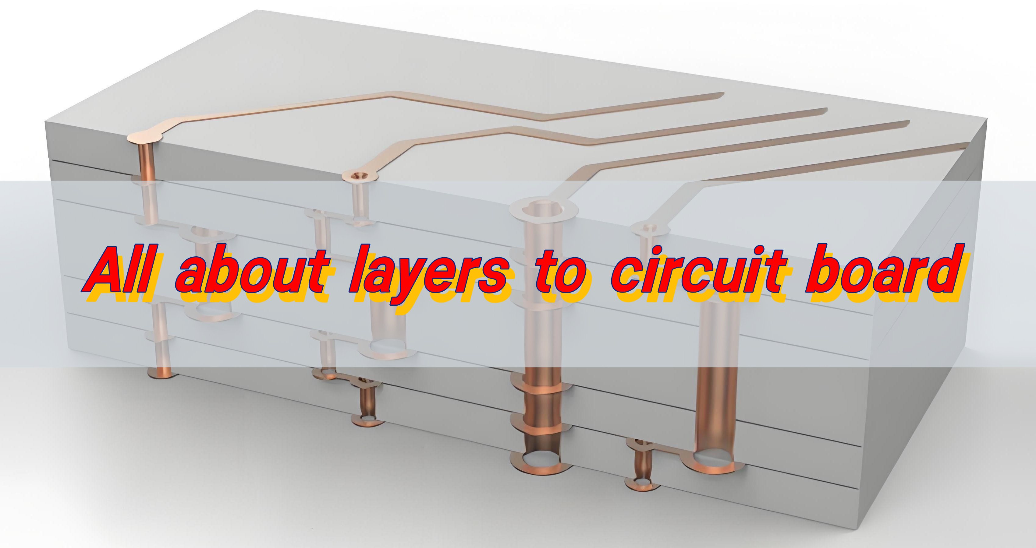
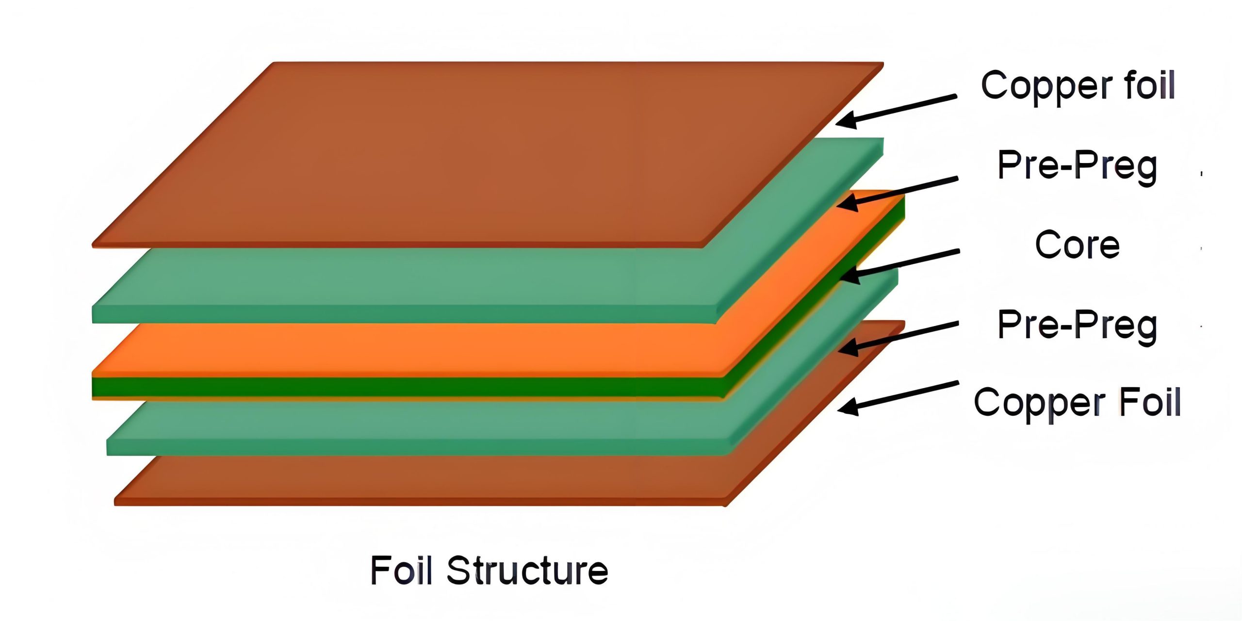
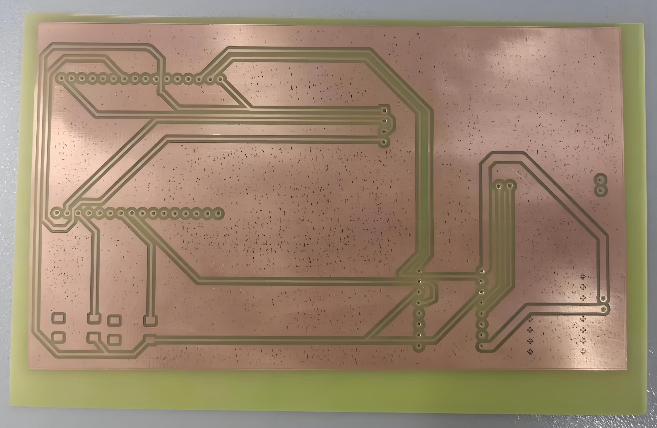
The core material of a PCB is copper clad laminate (CCL). Copper clad laminate plays a vital role in PCB manufacturing. It not only provides the functions of conductivity, insulation and support, but also directly determines the performance of PCB.
The manufacturing process of copper clad laminate includes impregnating electronic fiberglass cloth or other reinforcing materials with resin, then covering one or both sides with copper foil, and undergoing hot pressing. This material not only has the functions of conducting, insulating and supporting, but also serves as the core substrate of PCB.
In addition, other core materials of PCB include copper foil, prepreg, dry film and ink, etc. These materials together determine the quality and performance of the final product.
What is the copper plate on PCB?
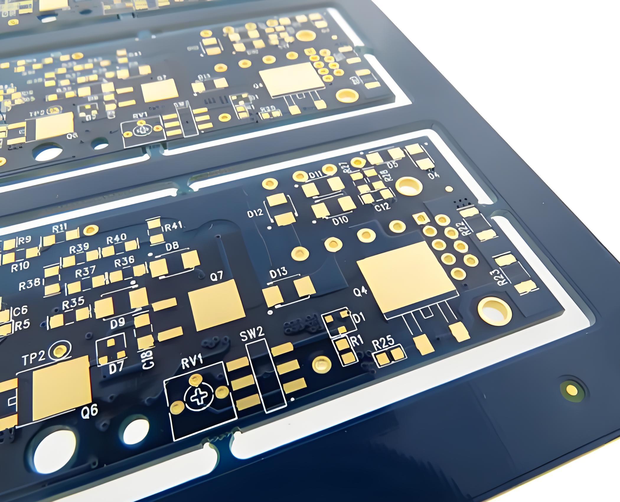
The copper clad laminate (CCL) on PCB is a composite material consisting of a non-conductive substrate (such as FR4) and one or more layers of copper foil. The copper foil is usually covered on one or both sides of the substrate for conductive connection.
Copper clad laminate plays a vital role in PCB manufacturing. It is the core material for making PCBs and has four major functions: conducting, insulating, supporting and signal transmission.
Copper clad laminate not only carries the connection between electronic components, but also ensures the normal operation of electronic equipment, and in the production of multilayer boards, it also plays the role of core board.
The manufacturing process of copper clad laminate mainly includes impregnating the reinforcing material with a resin binder, then covering the copper foil on one or both sides, and finally hot pressing. It occupies an important position in PCB manufacturing, and direct materials account for about 60% of the total cost of PCB. It has a wide range of applications and is commonly found in electronic products such as computers, computers, and mobile communications.
Why is copper used in a PCB?
The main reasons for using copper in PCBs include the following:
- Conductive properties: Copper is an excellent conductive material that can ensure that current flows smoothly on the PCB to meet the working requirements of electronic equipment.
- Heat dissipation: The high thermal conductivity of copper can effectively disperse heat to a larger area, reduce local hot spots, and improve overall heat dissipation efficiency.
- Mechanical stability: Copper plating helps maintain the uniformity of lamination during PCB manufacturing and reduce deformation caused by uneven materials, thereby improving the mechanical stability of the finished product.
- Signal integrity: Copper plating can provide a low-impedance return path, reduce signal loss and interference, especially in high-frequency digital signal transmission, and improve the stability and reliability of signal transmission.
- Electromagnetic shielding: Large areas of ground or power copper plating can serve as a natural electromagnetic shielding layer to reduce external interference, while suppressing noise propagation within the circuit to meet EMC requirements.
- Reduce costs: Although the cost of copper is relatively high, its excellent electrical and thermal conductivity makes the circuit design more concise, reduces the number and complexity of components, and thus reduces the overall cost to a certain extent.
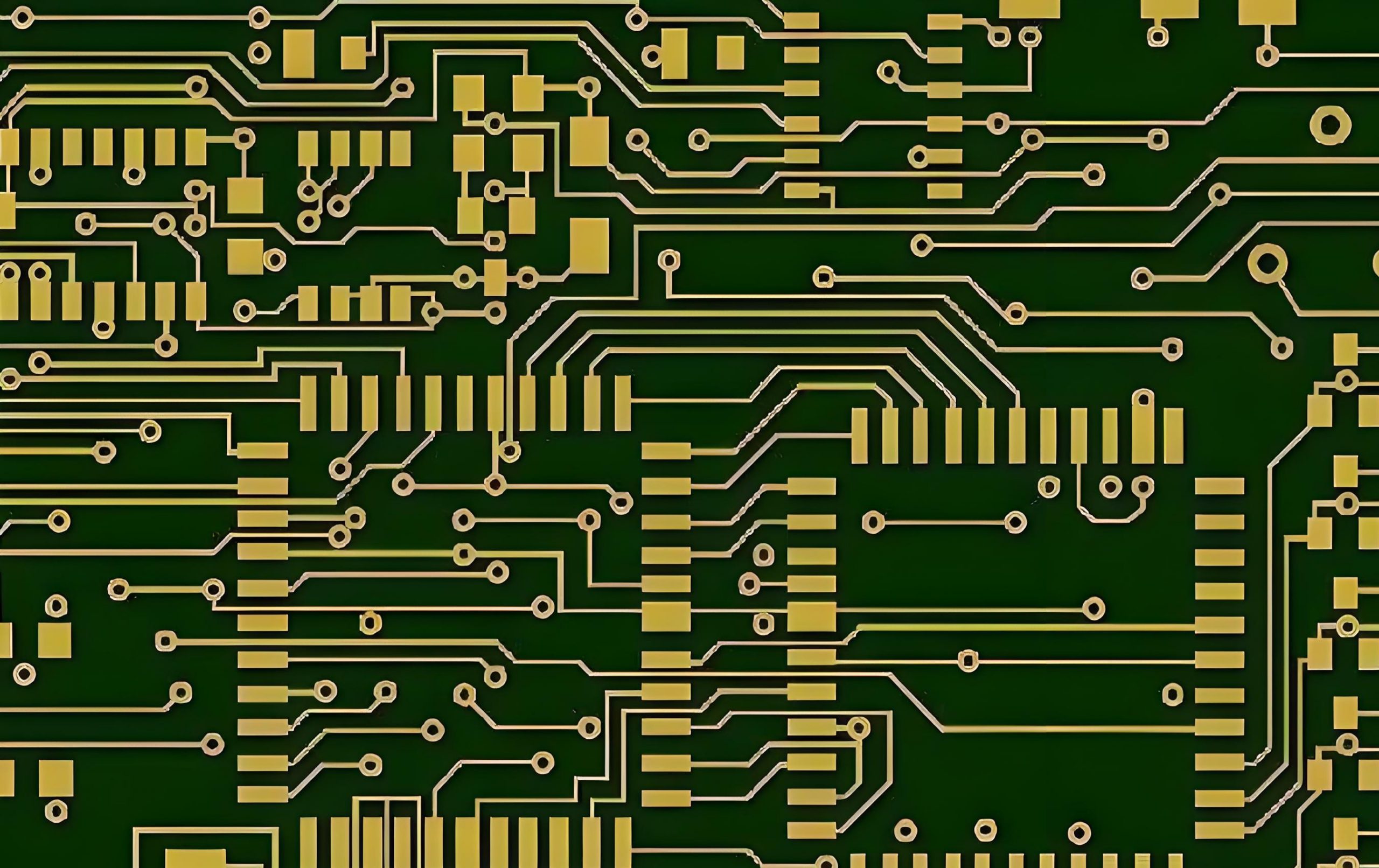
What is the purpose of copper traces on a PCB?
Copper traces on a PCB have a variety of uses, mainly including conduction, heat dissipation, mechanical support and signal transmission.
- Conductivity: Copper traces are the most important conductive material in PCBs, used to connect various components in the circuit, such as integrated circuits, resistors, capacitors, etc., to ensure smooth transmission of current.
- Heat dissipation: Copper has good thermal conductivity. By laying copper traces near the heat source, heat can be effectively dispersed, local overheating can be prevented, and the overall heat dissipation efficiency of the PCB can be improved.
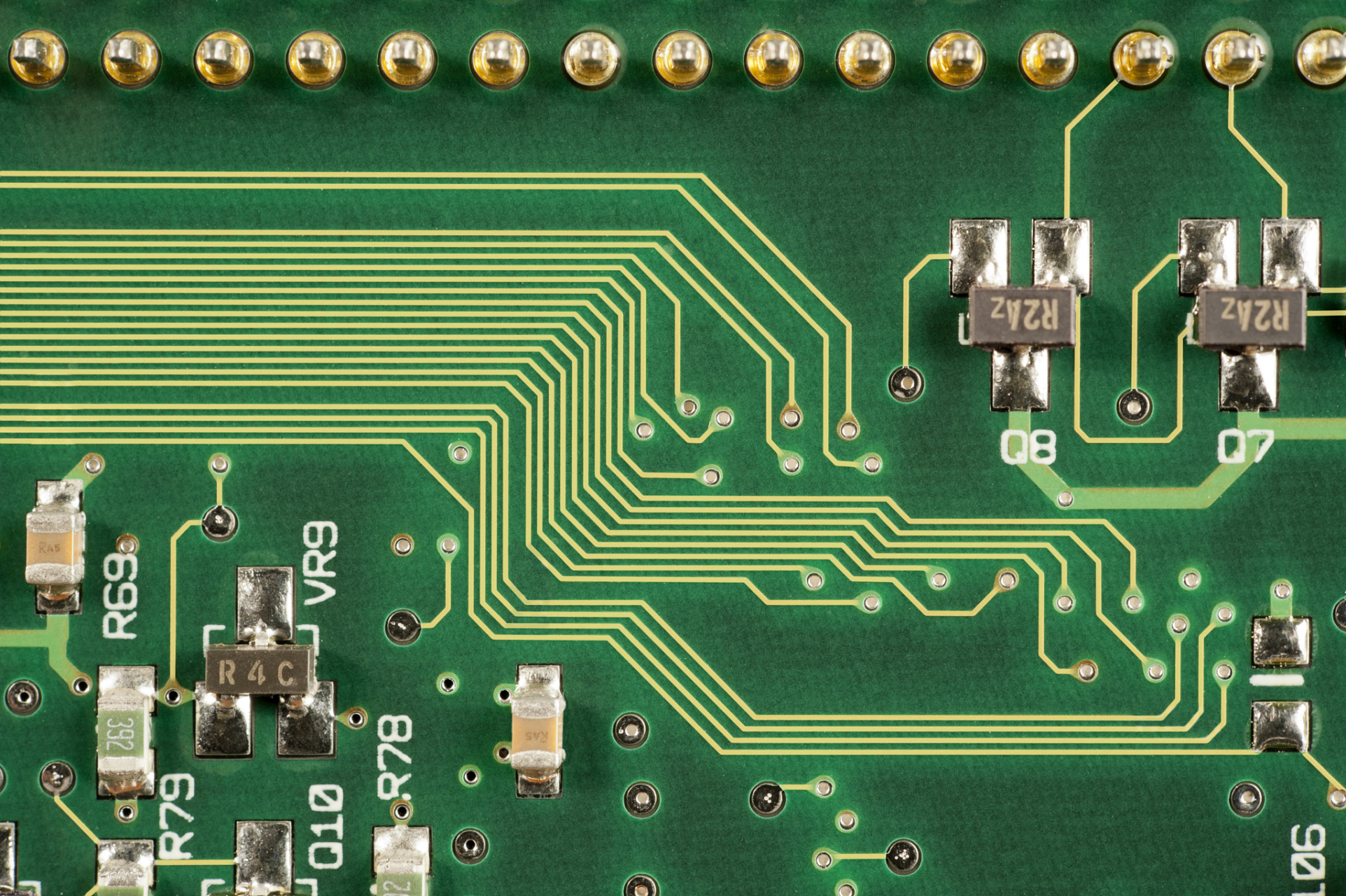
- Mechanical support: Copper traces play a supporting role in the PCB manufacturing process, helping to maintain the uniformity of lamination and reduce deformation, thereby improving the structural stability of the PCB.
- Signal transmission: In high-frequency circuits, copper traces provide a complete return path for high-frequency signals, reduce signal interference, and improve the stability and reliability of signal transmission.
How thick is 1 oz copper PCB?
The thickness of 1 oz copper PCB is about 1.4 mils, or 0.035 mm.
Key information is as follows:
- Relationship between ounces and thickness: In PCB manufacturing, the thickness of copper is usually expressed in ounces. 1 ounce of copper means that the weight of copper is 1 ounce in an area of 1 square foot.
- Unit conversion: After conversion, the thickness of 1 oz copper is about 1.4 mils, and 1 mil is equal to 0.001 inches, which is further converted to millimeters, that is, 0.035 mm.
What is the difference between 1 oz and 2 oz copper?
The main difference between 1 oz and 2 oz copper is their thickness and weight.
1. Thickness difference:
- 1 oz copper: The thickness of 1 oz copper is about 0.0356 mm or 1.35 mils.
- 2 oz copper: The thickness of 2 oz copper is about 0.0712 mm or 2.72 mils.
2. Weight difference:
- 1 ounce copper: 1 ounce is approximately equal to 28.35 grams (g).
- 2 ounces copper: 2 ounces is approximately equal to 56.7 grams (g), which is twice that of 1 ounce copper.
3. Application scenarios:
- 1 ounce copper: Usually used for general circuit board design, suitable for most electronic devices.
- 2 ounces copper: Suitable for applications that require higher current carrying capacity or higher reliability, such as servers, industrial control equipment, etc.
4. Cost difference:
- Increased thickness: Generally, increased copper thickness leads to higher costs because more materials and more complex manufacturing processes are required.
On the whole, the choice of copper in PCB is inevitable. With its excellent performance, it ensures stable signal transmission, anti-interference, efficient heat dissipation, circuit stability, high current carrying and enhanced PCB mechanical strength of electronic equipment, thereby ensuring reliable operation of the equipment.