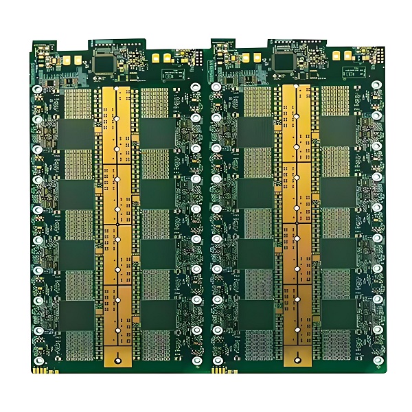
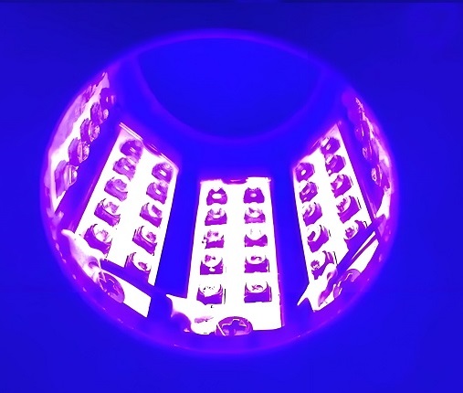
Metal Core Printed Circuit Boards (MCPCBs) are widely used in high-power applications like LED lighting, automotive systems, and power electronics. They offer superior thermal management compared to standard FR4 PCBs, but several variables impact their final pricing. Whether you’re prototyping or placing a volume order, understanding these factors helps you make informed decisions and avoid unexpected costs.
At EBest Circuit (Best Technology), we manufacture a wide range of MCPCBs tailored to customer requirements. Below, we’ve broken down the main elements that influence pricing so you can better evaluate your design options.
Key Technical Factors That Affect MCPCB Pricing
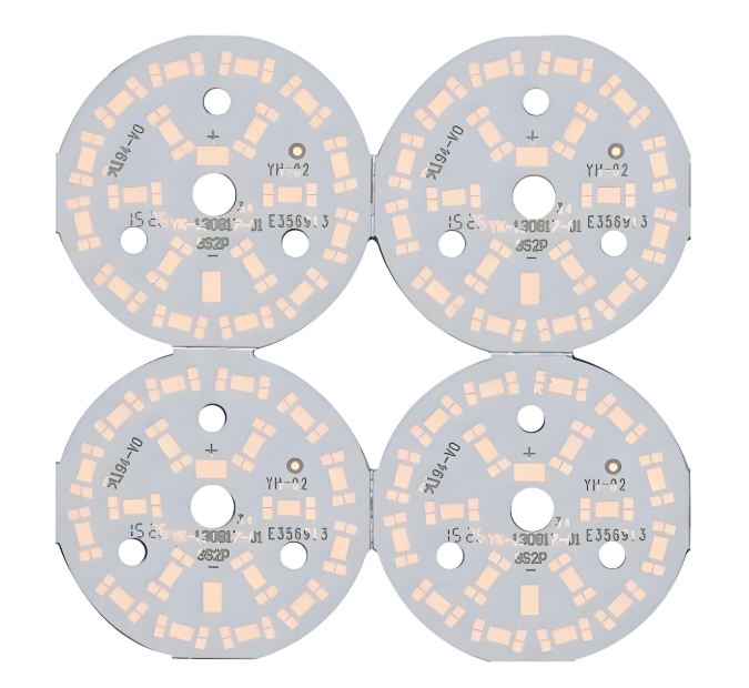
1. Board Dimensions
Size is the starting point for cost evaluation. For non-rectangular shapes like circles, pricing is based on the longest two sides—typically the diameter for round boards. Larger boards require more base material and longer processing time, which increases the unit price.
2. Copper Thickness
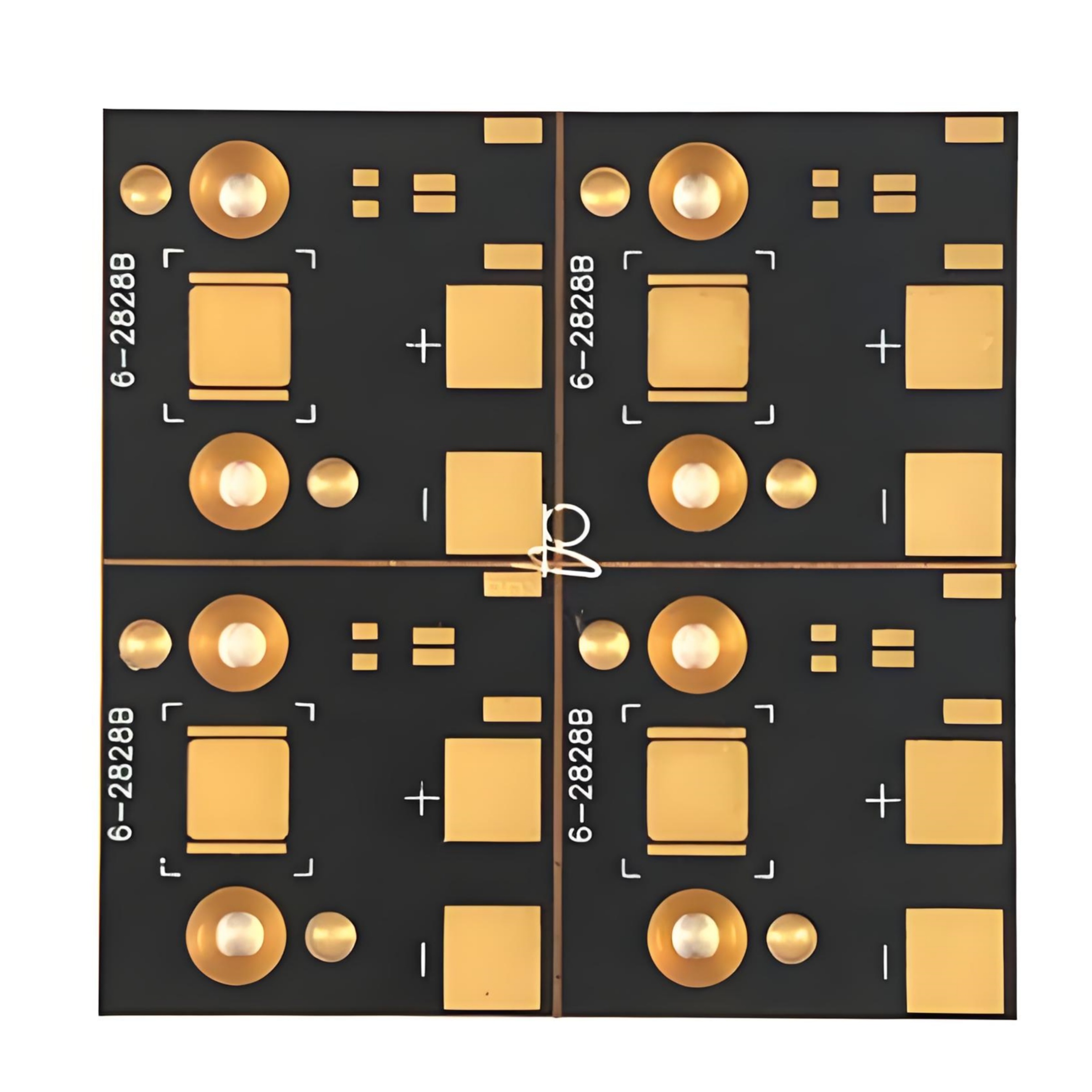
Copper thickness directly affects both thermal performance and cost. We offer standard and high-current options, including 0.5 OZ, 1 OZ, 2 OZ, 3 OZ, up to 8 OZ. Thicker copper enhances current-carrying capacity but also raises the complexity and expense of manufacturing.
3. Thermal Conductivity
A higher thermal conductivity helps to dissipate heat more efficiently. For example, 3W/m·K materials offer better heat transfer but are more expensive than standard options. The choice often depends on the power density of your application.
4. Surface Finishing
We support finishes such as HASL_LF (lead-free hot air leveling), OSP (Organic Solderability Preservative), and ENIG (Electroless Nickel Immersion Gold). ENIG is the premium choice due to its excellent solderability and oxidation resistance, though it comes at a higher cost.
5. Board Thickness
The most common MCPCB thickness is 1.6mm ±10%, which meets most design standards. Boards thinner than 1mm or thicker than 2mm will cost more due to non-standard processing. Our maximum capacity reaches 4.0mm ±10% for specific projects.
6. Solder mask Type and Color
Solder mask adds not only a protective layer but also an aesthetic touch. We offer white, black, blue, green, and red options. For high-end applications like LED boards, Taiyo solder mask is preferred for its excellent reflectivity, though it is priced higher than regular options.
7. Stack-Up and Construction
The complexity of the PCB stack-up has a big impact on both cost and manufacturing time. Single-layer boards are simpler and cheaper, while multi-layer, double-sided, or heat sink-integrated boards increase the number of processes, materials, and quality inspections required.
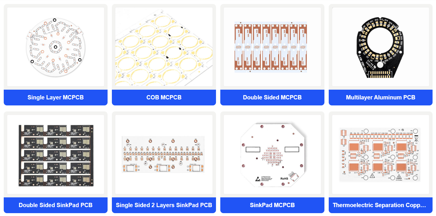
MCPCB Types We Offer
Our company specializes in producing a wide range of MCPCB types to suit various thermal and mechanical requirements:
Single Layer MCPCB
Two Layers MCPCB
Double-Sided MCPCB
Multi-Layer MCPCB
Chip-on-Board (COB) MCPCB
Heat Sink Integrated MCPCB
Each type is customizable to your exact application needs—whether you’re building high-power LED lighting, automotive electronics, or power conversion devices.
How to Choose the Right Parameters Without Overspending?
When planning your MCPCB project, it’s essential to balance performance requirements with budget constraints. Here are a few suggestions:
Match copper thickness to your current needs – don’t over-specify if lower OZ will suffice.
Select surface finishing based on reliability needs – use ENIG for sensitive components, OSP for more budget-friendly builds.
Ask about solder mask options early – especially for LED projects requiring high reflectivity.
Consider standard thicknesses – unless your application has unique structural or thermal demands.
Let us help with stack-up decisions – especially for complex or multi-functional boards.
At EBest Circuit (Best Technology), we guide you through each stage of development, offering design support, material recommendations, and volume-based quotations that match your project goals.
Need help optimizing your MCPCB design for performance and cost?
Contact our team today for a fast, professional quote and expert guidance tailored to your application.
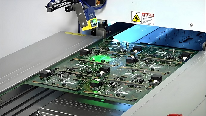
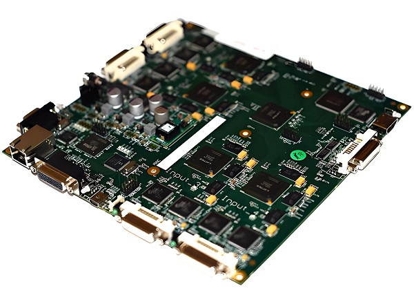
PCB contract manufacturing is a process where companies outsource the production of printed circuit boards to a third-party manufacturer. This includes not just making the board, but also assembling components, running functional tests, and sometimes even final product packaging. It allows companies to focus on core tasks like product development and marketing, while the technical side of electronics production is handled by experts.
At its core, PCB contract manufacturing saves time, reduces production costs, and ensures consistency in quality. For startups and global electronics brands alike, finding a dependable contract manufacturer can significantly boost speed-to-market and reduce project risks.
What Is PCB Contract Manufacturing
Our Printed Circuit Board Services
At EBest Circuit (Best Technology), we offer a complete range of services under one roof. Whether you’re developing a new electronic product or scaling up production, we handle everything from the initial design to final functional testing. Here’s what we bring to the table:
PCB Layout & Design
We help you start from scratch or improve your existing Gerber files. Our layout team is experienced in high-density routing, impedance control, and EMC-compliant designs. With tools like Altium Designer and CAD, we ensure accurate and efficient PCB layouts tailored to your project needs.
OEM & ODM PCB Manufacturing
Whether you need OEM or ODM service, we have the capability to take your concept and turn it into a working product. Our engineering team collaborates closely with clients to deliver custom solutions that are production-ready.
Electronic Components Assembly
From SMT (Surface Mount Technology) to through-hole assembly, our facility is equipped for full-scale PCBA (Printed Circuit Board Assembly). We support both leaded and RoHS-compliant assembly and offer automated inspection (AOI), X-ray, and BGA rework services to guarantee every joint is solid and reliable.
Wire Harness Assembly
We also supply PVC/PE/TPU/LZSH hook-up wire, flat cable, connector wire harness for machinery equipment, and cables for the field of electronic appliances, DC power supply, audio video devices, toys, medical equipment, communication devices, electrician & electrical, computer accessories cable, and so on.
Box Building Assembly
We don’t stop at the board level. If you need enclosure integration, cable harnessing, or full unit assembly, our box building assembly service is available. This end-to-end solution simplifies your supply chain and gives you more control over the finished product.
Functional Testing
We provide full functional testing based on your test procedure or help you develop one. This includes power-on tests, signal integrity verification, and custom fixture testing. We ensure your board works perfectly before it reaches your customers.
Our Printed Circuit Board Services
What PCBs We Can Fabricate?
Our team at EBest Circuit (Best Technology) specializes in a wide range of printed circuit board types. No matter your project’s complexity or environment, we’ve got you covered. Here are some products that we can make, but not limited to these PCBs.
Extra Thin PCB
For devices that require tight packaging like smart cards, cameras, or medical sensors, we offer ultra-thin PCBs as thin as 0.1mm. These boards maintain strength while saving space.
HDI PCB
High-Density Interconnect (HDI) PCBs support advanced electronics with fine-pitch components, blind and buried vias, and micro-via-in-pad technology. These are perfect for smartphones, tablets, and compact IoT devices.
RF PCB
We manufacture RF (Radio Frequency) PCBs using low-loss materials like Rogers, Taconic, and PTFE laminates. These boards are designed for wireless communication, antennas, and radar systems, where signal clarity matters most.
Heavy Copper PCB & Busbar PCB
When high current is involved, such as in automotive or industrial power supplies, heavy copper and busbar PCBs are necessary. We can produce boards with copper thickness from 2oz to 20oz, ensuring excellent thermal and electrical performance.
Metal Core PCB
For LED lighting and power conversion applications, our metal core PCBs (MCPCBs) provide efficient thermal dissipation. Aluminum and copper cores are both available depending on your thermal and mechanical needs.
Ceramic PCB
Using materials like aluminum nitride and alumina, ceramic PCBs deliver outstanding heat resistance and insulation. We have mature manufacturing technologies, including: Thick film ceramic PCB, thin film ceramic PCB, AMB ceramic PCB, DBC & DPC ceramic PCB, HTCC & LTCC ceramic PCB.
Flex Circuit & Rigid-Flex PCB
Flex circuits offer excellent bendability, reducing connectors and saving space. Rigid-flex PCBs combine the best of both worlds and are widely used in wearables, drones, and other portable electronics.
High-Speed PCB
We design and produce high-speed PCBs with controlled impedance, low-loss materials, and proper stack-ups. These are ideal for applications like 5G networks, servers, and high-frequency digital communication.
High TG PCB
When operating temperatures exceed 170°C, High-TG (glass transition temperature) PCBs are the right choice. These boards are more stable thermally and mechanically, perfect for automotive and industrial applications.
IC Substrate
We also support packaging solutions with IC substrates that act as a bridge between chips and PCBs. Our substrates offer fine-line traceability and are used in semiconductor packaging.
Ceramic Packages
Ceramic packages provide superior hermetic sealing and thermal cycling endurance. These are used to package sensitive ICs in defense, aerospace, and critical medical applications.
FR4 PCB Capability in EBest Circuit (Best Technology)
At EBest Circuit (Best Technology), we offer a wide range of FR4 PCBs — the most common material in the PCB industry — from consumer electronics to industrial control systems and automotive electronics. Whether it’s single-sided, double-sided, or multi-layer (up to 40 layers), we provide:
✅ General Capabilities
Layer Count: 1–40 layers
Board Size: Up to 580mm × 1200mm
Board Thickness: 0.2mm to 3.2mm
Copper Thickness: 0.5oz to 6oz (outer), 0.5oz to 3oz (inner)
Finished Hole Size: ≥ 0.10mm
Minimum Line Width / Spacing: 3mil / 3mil (0.075mm)
Aspect Ratio: Up to 12:1
Impedance Control: ±10% or better
✅ Material Options
Standard FR4: Tg135°C
High-TG FR4: Tg170°C to Tg180°C
Halogen-Free FR4: Environmentally friendly for RoHS/REACH applications
Low Dk/Df FR4: For better signal performance in high-speed circuits
✅ Surface Finishes
HASL (Hot Air Solder Leveling) – Leaded & Lead-free
With a monthly capacity of over 30,000 square meters and a 98% on-time delivery rate, our FR4 line is built to serve both prototypes and mass production.
Certifications & Quality Assurance in PCB Manufacturing
At EBest Circuit (Best Technology), quality isn’t just a goal — it’s a standard built into every step of our manufacturing process. To ensure compliance with international regulations and industry-specific requirements, we maintain a comprehensive set of certifications, including:
ISO 9001:2015 – Quality Management System
ISO 13485:2016 – Medical Device Quality System
IATF 16949:2016 – Automotive Quality Management
AS9100D – Aerospace & Defense Quality Management
UL Certification
RoHS & REACH Compliance
IPC Standards Compliance – IPC-A-600 and IPC-A-610 Class 2 & Class 3 for PCBfabrication and assembly
One-Stop High-Quality PCB Contract Manufacturer
When you’re looking for a reliable partner to handle your PCB contract manufacturing, EBest Circuit (Best Technology) is ready to deliver more than just boards. We provide full-service support — from design to delivery — with speed, precision, and attention to detail.
We offer a complete solution that includes PCB fabrication, components sourcing, assembly, testing, and even box build — all under one roof. That means you don’t have to juggle multiple suppliers or waste time coordinating between factories. You get a dedicated project manager, clear communication, and consistent quality from start to finish.
Engineering Support: this isn’t traditional engineer support, in EBest Circuit (Best Technology), every sales are engineer, they are professional so that can save much time on design communication and can give you the best solutions.
Fast Turnaround: we offer quick-turn prototyping (as fast as 24 hours) and competitive lead times for volume production.
Global Shipping: Whether you’re in the US, Germany, Japan, or Australia, we ship your orders promptly with DHL, FedEx, UPS, air & ocean shipment.
Traceability System: Our ERP system keeps detailed records for every board we produce, offering transparency and traceability.
WIP Update Every Week: Every customer can enjoy one-to-one sales-assistant service, they will update the product status & share videos every week for you, so that you can closely to your PCBs.
Cost-Effective Solutions: With advanced production lines and a mature supply chain, we provide cost-effective options without sacrificing quality.
PCB contract manufacturing can significantly reduce your product development cycle and overhead. By partnering with a professional and certified provider like EBest Circuit (Best Technology), you ensure every step — from PCB layout to functional testing — meets your project goals with precision and speed.
Whether you need a simple FR4 board or a high-performance ceramic PCB, our comprehensive services and commitment to quality make us a trusted choice for businesses around the world.
Frequently Asked Questions
1. What industries does EBest Circuit (Best Technology) serve?
We serve a broad range of industries including medical, automotive, aerospace, telecom, and consumer electronics.
2. Can EBest Circuit (Best Technology) support low-volume or prototype orders?
Yes, we support both small-batch prototypes and high-volume production with flexible minimum order quantities.
3. Do you offer component sourcing services?
Absolutely. We have partnerships with authorized distributors to source genuine components and manage the BOM for you.
4. What file formats do you accept for PCB layout?
We accept Gerber, ODB++, and other formats such as Altium, Eagle, and CAD-based files.
5. How can I request a quote for PCB contract manufacturing?
Simply send your files and requirements via our online form or email, and our sales team will get back to you within 24 hours.
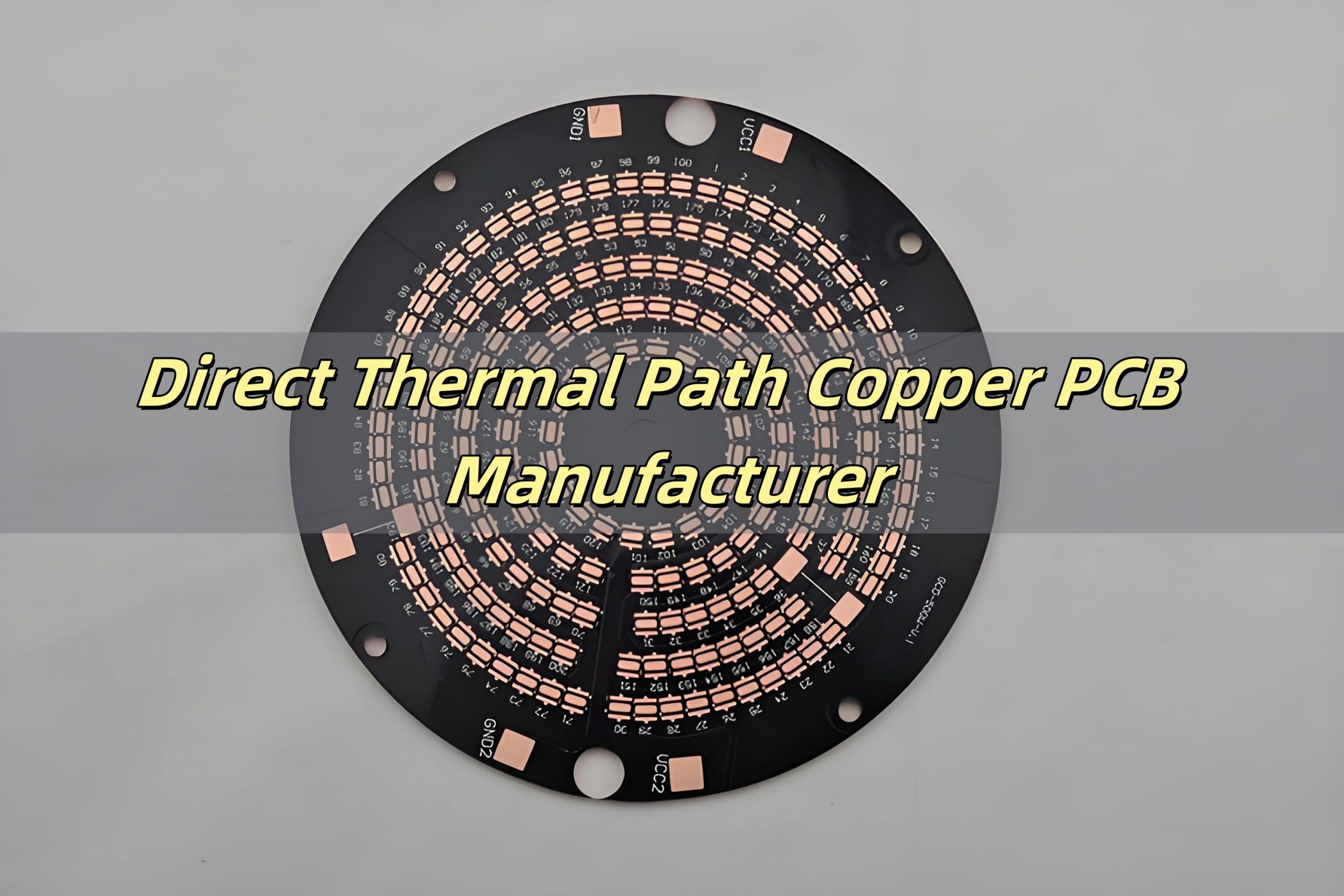
A Direct Thermal Path Copper PCB, also called DTP copper PCB or sinkpad copper base PCB. It is a type of high-performance circuit board used in applications where heat dissipation is critical. Unlike standard printed circuit boards (PCBs), which rely on dielectric layers to insulate the copper circuitry from the metal base, a DTP PCB removes this insulation layer directly beneath the heat-generating components. This creates a direct connection between the component, the copper layer, and the copper base.
This structure allows heat to flow quickly and efficiently away from the source, reducing thermal resistance and improving the performance and reliability of electronic components, especially in high-power or high-current environments. These boards are widely used in LED lighting, automotive systems, telecom infrastructure, and power electronics.
Why Thermal Management Matters in Electronics?
Every electronic device generates heat when it’s running. While small gadgets like phones may only get warm, high-power devices like industrial lighting systems or motor controllers can heat up rapidly. If this heat isn’t removed effectively, it can cause serious problems:
Component failure
Reduced lifespan of electronic parts
Malfunction due to overheating
Safety risks, especially in automotive or aerospace applications
To prevent these outcomes, thermal management becomes a critical aspect of PCB design. Engineers use a combination of heat sinks, thermal vias, and copper planes—but in extreme conditions, these are often not enough. That’s where DTP copper PCBs come in—they allow maximum heat transfer from hot components to the surrounding environment, helping electronics run cooler and more reliably.
Features of DTP Copper PCB
Direct thermal path copper PCBs stand out due to their special construction and capabilities. Here are some of their key features:
Thick copper base (up to 10 oz or more): Helps carry more current and draw heat away quickly.
Direct contact between copper circuit and metal base: Eliminates the thermal barrier of dielectric materials.
Excellent heat dissipation: Thermal resistance is significantly lower compared to regular MCPCBs.
Strong mechanical structure: Supports heavy components without deformation or cracking.
Stable performance in harsh environments: Suitable for high-temperature, vibration, and high-voltage conditions.
These features make DTP PCBs a practical choice for demanding applications where standard PCBs would overheat or fail.
How Does DTP PCB Work?
The principle behind a DTP PCB is simple: remove the thermal barrier (dielectric layer) between the heat source and the metal base. In a typical metal core PCB, the heat generated by a component passes through a dielectric layer (which is an electrical insulator) before reaching the metal base. This dielectric slows down the heat transfer.
In a DTP PCB, the designer removes the dielectric material under the power component and creates a direct copper pad that touches the metal base directly. This structure dramatically reduces thermal resistance and allows heat to flow out much faster.
In short, DTP PCBs give heat a shortcut—a direct path to escape—leading to lower operating temperatures and better performance.
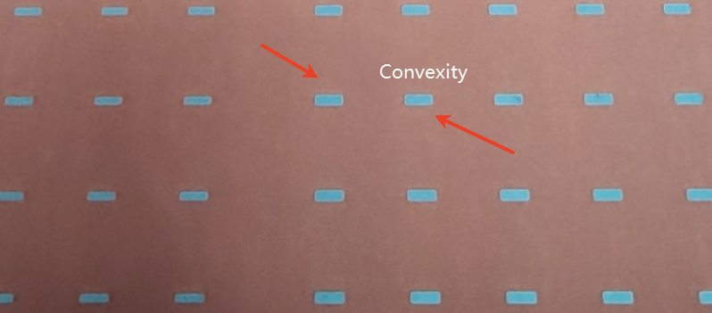
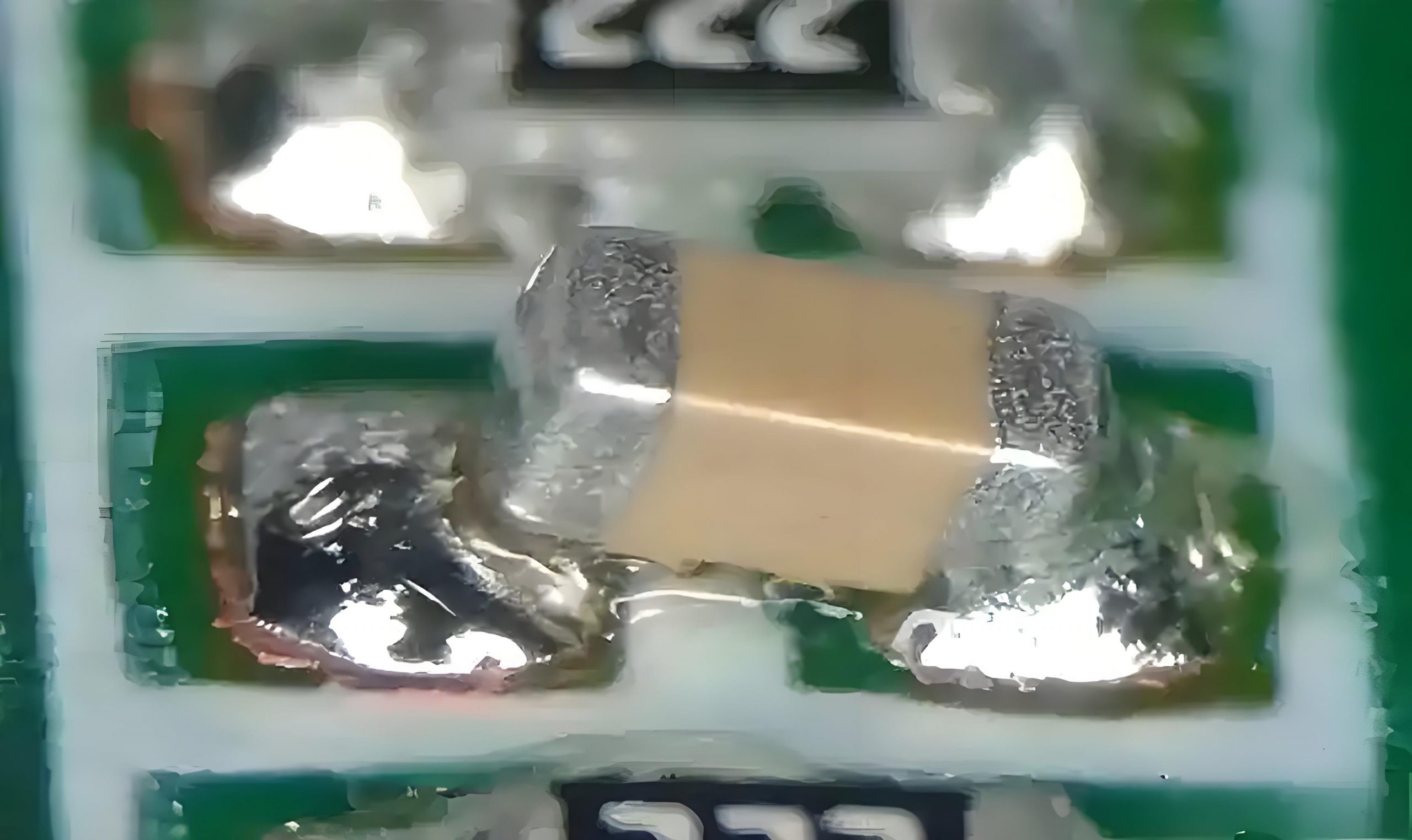
How Does the Convexity Pad Create?
The convexity pad is a small bump or raised copper structure that connects the top copper circuitry directly to the metal base below. This feature is critical in DTP PCBs because it serves as the contact point for heat transfer. Actually, the convexity pad is a little complicated than normal. Normally the thickness of copper core/substrate is 0.8mm, 1.0mm, 1.2mm, 1.4mm, 1.6mm, 2.0mm. And there’re blue protection film on both sides. We will remove that protection film after raw material cutting, before convexity making, so that copper can be etched. After that, we will grind the copper core to make sure it’ll be clear enough, so that in next step another film can be added to make trace.
Then, we will add one extra layer of film (normally blue color, and will refer to blue film hereafter) on whole area copper core, and after developing & etching, only selected area of blue film will be kept and other area will be removed away. In fact, the area of blue film will be the place convexity will be.
Why Aluminum Base Is Not Suitable to Make DTP PCB?
As we know, the convexity pad directly connects the copper base serving as the substrate to the thermal pads of the LED without any insulating thermal conductive material in between. In this way, the heat from the LED can be directly transferred to the copper substrate of the base through the solder, without having to pass through the electrical traces on the base surface and the insulating materials for heat transfer. This is why DTP PCB also is called thermoelectric isolation as well. (The heat output path of the LED is directly connected to the copper plate and separated from the electrical traces). As for why aluminum substrates cannot be used, it is because the heat pads of the led chips need to be directly soldered to the copper substrate through the solder on the reserved protrusion on the base, and aluminum doesn’t bond well with standard solder materials.
In addition to this, some manufacturers said they can make DTP aluminum PCB. Maybe they indeed made it, but need to spend a lot of time and the cost is much higher than DTP copper base PCB. And compared with copper base PCB, the thermal conductivity of aluminum PCB is slightly lower, so we always not recommend customers to make DTP aluminum PCB.
Considerations While Using Direct Thermal Path MCPCB
Before incorporating DTP copper PCBs into your design, keep these factors in mind:
1. Component Placement
Ensure components that generate high heat are directly above the DTP pads. Misalignment can compromise thermal efficiency.
2. Base Thickness
The thickness of the copper base affects both heat transfer and mechanical strength. Heavier bases improve heat conduction but may reduce flexibility.
3. Thermal Simulation
Use thermal analysis software to simulate heat dissipation before production. This helps identify hotspots and optimize layout.
4. Dielectric Material
Where dielectric is still used, choose materials with high thermal conductivity (such as ceramic-filled polymers).
5. Mounting & Enclosure
DTP PCBs perform best when mounted to a heatsink or metal enclosure. Make sure there’s good thermal interface material between them.
6. Surface Finish
Use finishes like ENIG (Electroless Nickel Immersion Gold) or OSP (Organic Solderability Preservative) to improve soldering and surface protection.
DTP Copper PCB Manufacturing Process
Manufacturing a direct thermal path copper PCB requires careful attention and precision. Here’s a step-by-step breakdown:
Step 1: Base Metal Selection
A thick copper base (typically 1.6–3.2 mm) is chosen as the base layer. This base serves as the thermal sink for the entire board.
Step 2: Lamination
A high-thermal conductivity dielectric is laminated to the copper base. This is done only where insulation is needed.
Step 3: Circuit Layer Preparation
A copper foil (typically 1–3 oz) is applied on top. The PCB manufacturer then performs photolithography and etching to define the circuit pattern.
Step 4: Dielectric Removal
The dielectric under high-heat components is selectively milled or punched to expose the copper base.
Step 5: Convex Pad Formation
Using precision CNC machining, a raised copper pad is formed on the exposed area. This pad directly contacts the component’s thermal pad.
Step 6: Surface Finishing
The board receives a protective finish like ENIG, OSP, or immersion silver to prevent oxidation and improve solderability.
Step 7: Solder Mask and Silkscreen
Solder mask is applied to protect the circuitry, followed by silkscreen for labeling.
Step 8: Testing and Quality Control
Each board undergoes electrical and thermal testing to ensure performance, conductivity, and durability.
This manufacturing process results in a high-performance PCB that can handle extreme heat conditions with ease.
Common Applications of DTP MCPCB
Because of their outstanding heat management, DTP copper PCBs are widely used across industries that rely on high-power or high-brightness components. Here are some key applications:
Automotive LED lighting: Headlights, brake lights, and DRLs require efficient thermal dissipation to maintain brightness and longevity.
Power electronics: DTP PCBs are used in DC/DC converters, motor controllers, and battery management systems for better heat control.
Industrial lighting: High bay and floodlights benefit from improved thermal design to prevent premature failure.
Telecommunication systems: Base stations and network equipment use DTP PCBs to manage heat from amplifiers and processors.
Aerospace and defense: Systems in satellites and aircraft need PCBs that perform reliably under thermal and environmental stress.
Wherever performance and reliability are non-negotiable, DTP copper PCBs are a trusted solution.
FAQs About Direct Thermal Path MCPCB
Q1. What makes DTP PCBs different from regular MCPCBs?
The key difference is the removal of the dielectric layer beneath the component, enabling direct heat flow from the copper pad to the metal base. This dramatically improves thermal conductivity.
Q2. Can DTP copper PCBs be used in multilayer stackups?
Typically, they are single-sided. However, hybrid multilayer configurations are possible for complex applications, though they require advanced design and manufacturing techniques.
Q3. Is copper the only metal used for DTP base material?
In high-end applications, copper is the preferred base due to its superior conductivity and durability. Aluminum is cheaper but less effective in DTP designs.
Q4. Do I still need a heatsink with a DTP PCB?
Yes, in most cases. While the DTP board efficiently moves heat to its base, the heat still needs to exit the board—often through a heatsink or the product’s metal housing.
Q5. How can I get a DTP copper PCB made?
You’ll need a PCB manufacturer like EBest Circuit (Best Technology) that specializes in metal core PCBs and has equipment for precision CNC milling and selective dielectric removal. Request thermal simulation support for best results.
If you’ve ever held a green circuit board, chances are you were looking at an FR4 PCB. It’s one of the most common materials used in printed circuit board production today. But what makes FR4 so popular? And how exactly does the FR4 PCB manufacturing process work from start to finish?
In this guide, we’ll walk you through everything from the basics of FR4 material to the full production process, FR4 PCB stack-up design, material properties, and key manufacturing considerations. Whether you’re a designer, engineer, or purchasing specialist, this is your go-to reference for working with FR4 PCBs.
What Is FR4 Material?
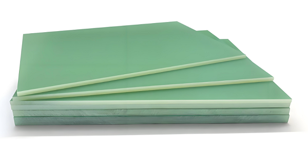
FR4 stands for “Flame Retardant 4.” It is a type of fiberglass-reinforced epoxy laminate that meets specific flame resistance standards. The core of the material is made from woven fiberglass cloth soaked in epoxy resin. This combination gives it excellent mechanical strength and insulation.
It offers great mechanical strength and excellent insulation, even at high temperatures. Because of these qualities, FR4 PCB material is widely used in everything from mobile phones and automotive systems to medical devices and industrial controls.
FR4 PCB Material Properties
The performance of any PCB starts with the base material. Here’s what makes FR4 PCB material properties suitable for a wide range of electronics:
Electrical Insulation: FR4 is an excellent electrical insulator, which protects your circuit.
Heat Resistance: It can withstand soldering and other high-temperature processes.
Mechanical Strength: Its fiberglass base provides structural durability.
Moisture Resistance: FR4 doesn’t absorb much water, so it remains stable in humid conditions.
Thermal Stability: Most FR4 materials can handle temperatures up to 130–140°C. Some high-Tg versions go higher.
FR4 PCB Stack-up
The stack-up refers to how the layers of copper and insulating materials are arranged in a PCB. In FR4 PCBs, the stack-up directly affects signal performance, EMI control, and even thermal management. A typical FR4 PCB stack-up can have one, two, or multiple copper layers separated by dielectric layers of FR4.
A basic FR4 PCB stack-up might include:
Top Copper Layer (signal)
Prepreg layer (dielectric made of FR4)
Inner Copper Layer (for power or signal routing)
Core (FR4 material with copper on both sides)
Bottom Copper Layer
For multilayer boards, additional layers are added between the top and bottom layers using alternating layers of copper and FR4-based dielectric.
Engineers design the stack-up based on signal integrity, board thickness, and power distribution requirements. Choosing the right arrangement improves reliability and helps prevent signal interference.
FR4 PCB Thickness
One important design decision is selecting the right FR4 PCB thickness. Standard boards are often 1.6 mm thick, but other options are available, ranging from 0.2 mm to over 3.2 mm.
FR4 boards typically come in standard thicknesses such as:
0.4 mm
0.8 mm
1.0 mm
1.2 mm
1.6 mm (most common)
2.0 mm
Custom thicknesses are also available depending on the application. Thicker boards are ideal for mechanical strength and high-current applications, while thinner boards are used in compact devices like smartphones.
When choosing FR4 PCB thickness, consider the following:
Mechanical strength: Thicker boards provide more durability.
Flexibility: Thinner boards can reduce weight and size.
Thermal load: More copper and greater thickness help dissipate heat.
Signal integrity: The distance between signal layers matters in high-speed designs.
Proper thickness planning improves performance and reduces warping during reflow or wave soldering.
What Is the Difference Between FR4 and FR5 PCB?
At first glance, FR4 and FR5 materials might seem very similar—they’re both fiberglass-based substrates. However, the key difference lies in their thermal performance.
Property
FR4
FR5
Max Temp. Resistance
~130–140°C
~170–180°C
Cost
Lower
Higher
Application
General electronics
High-temp environments
Dielectric Strength
High
Comparable to FR4
FR5 is a more heat-tolerant version of FR4 but also more expensive. Unless your project involves high temperatures, FR4 will typically be the better option. Most consumer and industrial electronics use FR4 unless extreme thermal demands require upgrading to FR5.
FR4 PCB Manufacturing Process – Step by Step
Now that we’ve covered the material, stack-up, and design considerations, let’s explain the whole FR4 PCB manufacturing process.
1. Material Preparation
Manufacturing starts with selecting the right FR4 board based on the desired thickness and copper weight. Sheets are cut into panels and cleaned for processing.
2. Inner Layer Imaging
For multilayer PCBs, inner copper layers are etched first. A photoresist is applied, and the circuit pattern is transferred using UV light. Unwanted copper is etched away using a chemical solution.
3. Layer Alignment & Lamination
Once inner layers are etched, layers are stacked with prepreg (uncured FR4 resin sheets) between them. This stack is laminated under heat and pressure to bond all layers together.
4. Drilling
Next, holes are drilled for vias and through-hole components. High-speed CNC machines or laser drills are used depending on the design.
5. Plating
Drilled holes are chemically treated and then electroplated with copper. This forms conductive paths between layers.
6. Outer Layer Imaging & Etching
Outer copper layers go through the same imaging and etching process as the inner layers. The circuit pattern is created using photoresist and chemical etching.
7. Solder Mask Application
A protective solder mask is applied to insulate copper traces and prevent solder bridges. This step also gives the board its green (or sometimes blue, red, or black) color.
8. Silkscreen Printing
Component labels and identifiers are printed on the board using white epoxy ink.
9. Surface Finish
Surface finishes like HASL, ENIG, or OSP are added to exposed copper pads. This step improves solderability and protects the copper.
10. Routing and V-Cutting
Boards are cut into their final shape using routers or V-cut machines.
11. Electrical Testing
Each board is tested for shorts, opens, and other faults using flying probe or fixture-based testers.
12. Final Inspection and Packing
Boards are visually inspected and packed in anti-static materials for delivery.
Considerations During FR4 PCB Manufacturing
There are several factors to keep in mind when manufacturing with FR4:
Thermal Expansion: Consider the coefficient of thermal expansion, especially for multilayer or BGA designs.
Glass Transition Temperature (Tg): Higher Tg FR4 is better for lead-free soldering and automotive applications.
Thickness Control: Even small deviations in FR4 PCB thickness can affect impedance and performance.
Copper Weight: Heavier copper requires more precise etching and lamination processes.
If you’re working with a reliable FR4 PCB manufacturer, these details are usually handled with strict quality controls.
Why Choose EBest Circuit (Best Technology) for Your FR4 PCB Manufacturing?
At EBest Circuit (Best Technology), we specialize in high-quality PCB manufacturing using FR4 material. Whether you need simple prototypes or complex multilayer designs, our team delivers consistent quality with fast turnaround. We use advanced MES systems to track your PCBs through every step of production, ensuring traceability and precision.
Multilayer PCB design is at the heart of compact, high-speed electronics. As more devices require higher functionality in smaller packages, multilayer PCBs have become the go-to solution. In this blog, we’ll explore how these boards are designed, what materials go into them, and how they are manufactured.
EBest Circuit (Best Technology) is a trusted PCB manufacturer based in China, specializing in small to medium-volume PCB fabrication, PCB assembly, and comprehensive electronic manufacturing services (EMS). As a one-stop PCB solutions provider, we go beyond manufacturing. Our services cover turnkey assembly, component sourcing, box build assembly, PCBA testing, and full electronics assembly. Whether you’re developing a prototype or scaling up to full production, EBest Circuit (Best Technology) is committed to delivering reliable quality, fast turnaround, and personalized support to meet all your PCB and electronics manufacturing needs.
What Is PCB Multilayer?
A multilayer PCB is a type of printed circuit board made by stacking multiple copper layers with insulating materials in between. While a single-sided PCB has only one conductive layer and a double-sided PCB has two, a multilayer PCB typically starts at four layers and can exceed thirty layers depending on the design complexity.
These copper layers are interconnected using vias (small plated holes). The main advantage is that multilayer PCBs allow more complex circuitry in a compact form. They’re used when simple routing becomes impossible due to high component density, high-speed signals, or design restrictions.
Multilayer boards usually contain signal layers, power planes, and ground planes that are symmetrically arranged to ensure electrical balance and mechanical stability.
Advantages of Multilayer PCB
There are many advantages of multilayer PCBs, especially for high-end, compact, and performance-driven applications:
High Circuit Density: Multilayer PCBs offer more real estate by using multiple layers. This helps route more connections without crowding.
Compact Size: By stacking layers, complex circuits can be condensed into smaller board sizes, which is important for modern gadgets.
Better Signal Integrity: Ground and power planes shield signal layers, helping reduce electromagnetic interference and signal loss.
Enhanced Reliability: Since many connections are internal and automated, multilayer PCBs tend to be more reliable than manually wired boards.
Improved Power Distribution: Dedicated power planes help distribute power evenly across the board.
Cost Efficiency in Mass Production: Although more expensive to design, they become cost-effective when produced at scale.
What Materials Are Used for Multilayer PCB?
Multilayer PCB construction involves several materials chosen based on the application’s electrical, thermal, and mechanical requirements. Common materials include:
Copper Foil: Used for all conductive layers. Thickness ranges from 0.5oz to 3oz, depending on current requirements.
Core Material (FR4): The most widely used substrate, made from fiberglass-reinforced epoxy. It provides mechanical strength and insulation.
Prepreg (Pre-impregnated resin): A resin-impregnated fiberglass that bonds layers together during lamination.
High-Frequency Materials: For applications like 5G or RF circuits, materials such as PTFE, Rogers, or ceramic substrates are used.
Solder Mask: This green or colored coating protects the board from oxidation and solder bridges.
Silkscreen: Printed on the board to mark component positions and labels.
For high-temperature or high-reliability applications, alternative materials like polyimide or metal cores may also be used.
Why Are There No 3 Layer PCBs?
Technically, you can make a 3-layer PCB, but they are very uncommon and often impractical. PCB manufacturing is designed to favor even-numbered layer configurations for several reasons:
1. Symmetry: Even-layered stack-ups offer better mechanical balance. Odd layers may lead to board warping due to uneven internal stress.
2. Manufacturing Simplicity: Most production lines are optimized for 4, 6, or 8 layers. A 3-layer board would require a custom process, which increases cost.
3. Signal Performance: High-speed signals benefit from a symmetrical structure. Odd-layer designs make it harder to maintain signal and power integrity.
Because of these reasons, designers usually move to 4-layer designs when they outgrow double-sided layouts.
How to Design a Multilayer PCB?
Designing a multilayer PCB starts with understanding the functional needs of your product. Here’s a step-by-step process:
Define Layer Count: Decide how many layers are required based on circuit complexity, signal integrity, and available space. Common configurations include 4, 6, and 8 layers.
Create a Stack-Up: Plan how each layer will function — signal, ground, or power. Layer arrangement impacts EMI performance and routing efficiency.
Component Placement: Place high-speed, sensitive, and power components with care. Keep analog and digital sections separate.
Routing Strategy: Route critical signals on inner layers to shield them from external noise. Use short, direct routes for clock and high-speed lines.
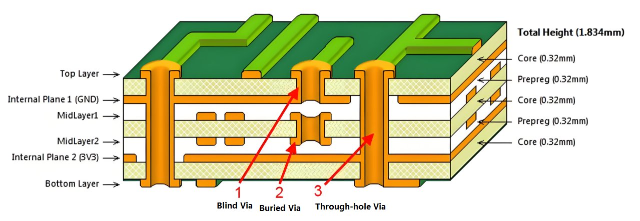
Via Planning: Use through-hole vias, blind vias, and buried vias to connect different layers.
Impedance Control: For high-speed signals, calculate and control the trace impedance using PCB design software.
Thermal Management: Add thermal vias and consider copper pour for better heat distribution.
Design for Manufacturability (DFM): Ensure trace widths, spacing, hole sizes, and clearances follow manufacturer guidelines.
Design tools like Altium Designer, Eagle, or KiCad can help streamline multilayer PCB design while checking for errors along the way.
How to Build a Multilayer PCB Stack-Up?
A stack-up is the arrangement of copper and dielectric layers in a multilayer PCB. It affects signal quality, EMI, thermal behavior, and mechanical strength.
Common 4-Layer Stack-Up:
Top layer: Signal
Inner layer 1: Ground
Inner layer 2: Power
Bottom layer: Signal
6-Layer Stack-Up Example:
Top: Signal
Layer 2: Ground
Layer 3: Signal
Layer 4: Signal
Layer 5: Power
Bottom: Signal
Tips for Effective Stack-Up:
Keep ground and power layers close for decoupling.
Place critical signals between ground planes.
Symmetry reduces warping.
Maintain consistent dielectric thickness to control impedance.
At EBest Circuit (Best Technology), our engineering team assists clients with stack-up planning to match their performance, size, and cost targets.
Multilayer PCB Manufacturing Process
The multilayer PCB manufacturing process involves combining multiple copper and insulation layers through precise steps:
1. Inner Layer Imaging
Each internal copper layer is printed with the desired circuit pattern using photoresist and UV light.
2. Etching
Unwanted copper is chemically etched away, leaving only the circuit traces.
3. Lamination
All layers are stacked with prepreg between them and laminated under high heat and pressure to form a single board.
4. Drilling
Holes are drilled through the stack to connect layers. These include through-hole, blind, and buried vias.
5. Plating
Copper is plated into drilled holes and on the board’s surface to create electrical paths.
6. Outer Layer Imaging and Etching
Outer layers undergo the same photoimaging and etching process as inner layers.
7. Solder Mask and Silkscreen Application
A solder mask is added to prevent oxidation and short circuits. Silkscreen is printed for component labeling.
8. Surface Finishing
Finishes like HASL, ENIG, or OSP are applied to pads for better solderability.
9. Testing and Inspection
Every board undergoes electrical tests and visual inspections to catch defects.
At EBest Circuit (Best Technology), we combine automated optical inspection (AOI), flying probe testing, and impedance measurement tools to ensure product quality at every stage.
Multilayer PCB Application
Multilayer PCBs are used in products where performance and miniaturization are critical. Here are some typical multilayer PCB applications:
Smartphones and Tablets: Compact devices need high-density PCBs to fit advanced features in tight spaces.
Medical Equipment: Imaging machines, heart monitors, and portable diagnostic tools depend on stable multilayer circuits.
Automotive Electronics: Modern vehicles use multilayer PCBs for infotainment systems, sensors, and control units.
Telecommunication Devices: Routers, switches, and 5G antennas rely on multilayer designs for signal integrity.
Industrial Controls: Multilayer PCBs support automation equipment and high-voltage circuits.
Military and Aerospace: Satellites, drones, and radar systems require rugged multilayer boards with excellent thermal and electrical performance.
How to Identify Multilayer PCB?
Identifying a multilayer PCB can be tricky just by looking at the surface. However, here are some tips:
Edge View: Under a magnifier, you can often see multiple stacked layers at the board edge.
X-ray Inspection: In factories, X-ray equipment can show internal connections and vias not visible from outside.
Blind/Buried Vias: If the board has vias that don’t go through the entire thickness, it’s likely multilayer.
Complexity and Component Density: A compact board handling many components usually suggests a multilayer design.
FAQs
1. What is the typical number of layers in a multilayer PCB?
Most commonly, multilayer PCBs have 4, 6, or 8 layers. High-end designs may go up to 32 or more.
2. Can multilayer PCBs be flexible?
Yes. Flexible multilayer PCBs are used in wearables, cameras, and aerospace applications where bending is needed.
3. Are multilayer PCBs expensive?
They cost more than single or double-layer PCBs but offer more value in space savings and performance.
4. What’s the difference between blind and buried vias?
Blind vias connect outer and inner layers. Buried vias connect internal layers only, and are hidden from the surface.
5. How does EBest Circuit (Best Technology) support multilayer PCB projects?
We offer complete support — design review, stack-up suggestions, high-speed materials, and full traceability via MES systems.
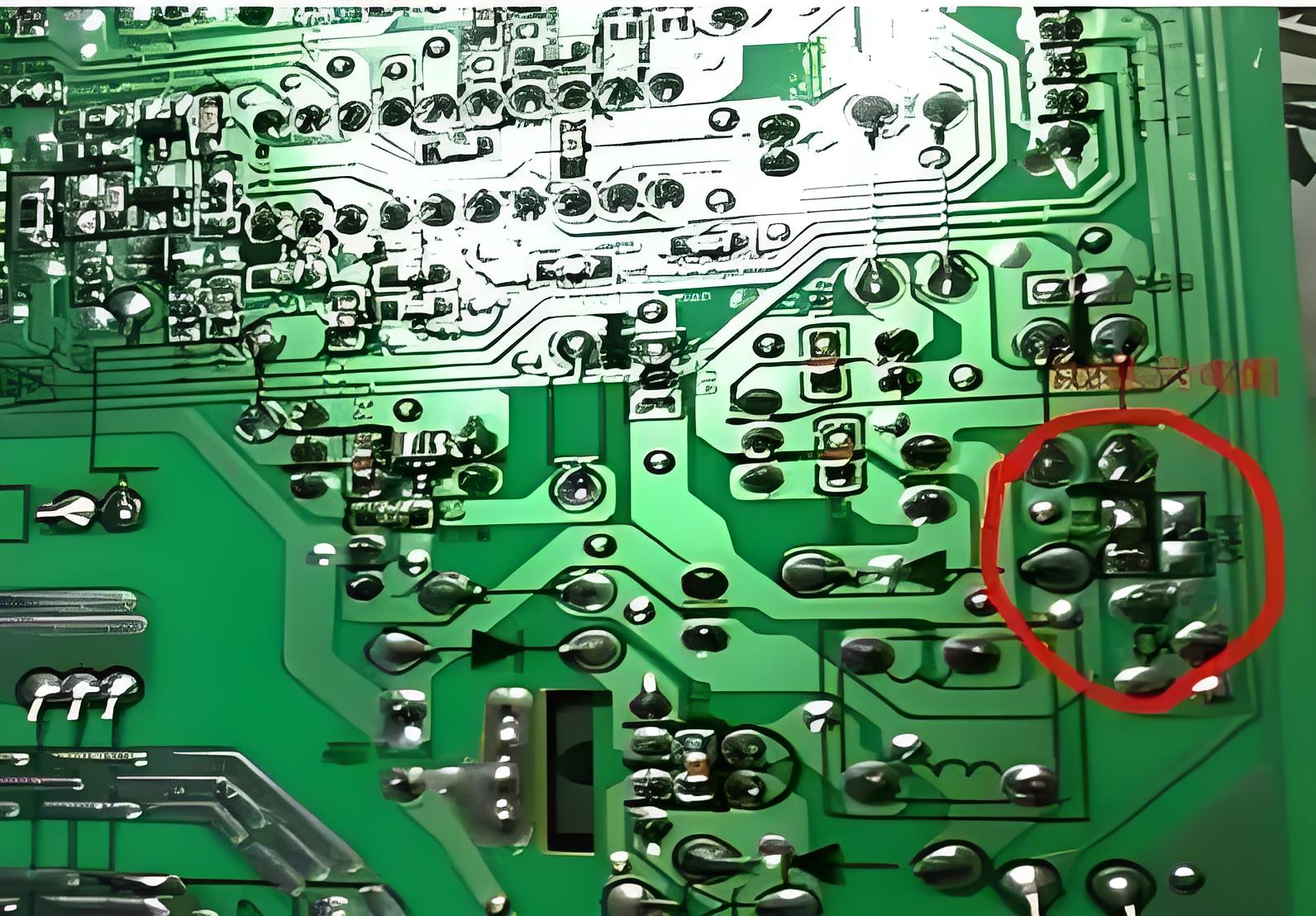
When a cold solder joint appears on a PCB, it might not fail immediately. But over time, it can cause real trouble—intermittent signals, unstable connections, or even complete circuit failure. These defects are often hidden, and if not caught early, they can waste time and money in rework.
In this blog, you’ll learn:
What a cold solder joint looks like
What causes it
How to avoid and fix it
Why a trusted PCB assembly partner like EBest Circuit (Best Technology) matters
What is a Cold Solder Joint?
A cold solder joint or cold joint solder, is a defective connection between a component lead or terminal and a PCB pad during PCB assembly process. Unlike a properly formed solder joint, which provides a strong, reliable electrical and mechanical connection, a cold solder joint fails to fully bond the two elements together.
When soldering is done correctly, the solder melts completely and wets both the component lead and the PCB pad, creating a smooth, shiny, and concave surface. In the case of a cold solder joint, however, the solder doesn’t reach its optimal melting point or doesn’t flow properly. This results in a rough, dull, and often uneven surface. The joint may look like it’s attached, but in reality, the connection is weak and prone to failure. It might conduct electricity intermittently or not at all, leading to erratic behavior in the electronic device, from occasional glitches to complete breakdowns.
Cold Solder Joint Causes
Several factors can contribute to the formation of cold solder joints. Understanding these causes is the first step in preventing them.
Inadequate Soldering Temperature
One of the primary culprits is insufficient soldering temperature. Each type of solder has a specific melting range, and if the soldering iron or reflow oven doesn’t reach and maintain the appropriate temperature, the solder won’t melt fully. For example, if the temperature is too low, the solder may only partially liquefy, leaving solid particles that prevent a proper bond.
Incorrect Soldering Time
If the soldering iron is applied for too short a time, the solder won’t have enough time to melt and flow properly. On the flip side, overheating the joint by leaving the soldering iron on for too long can also cause problems. It can damage the component leads, PCB pads, or even change the properties of the solder itself, potentially leading to a cold solder joint.
Poor Surface Preparation
The cleanliness and condition of the surfaces to be soldered are vital. If the component leads or PCB pads are dirty, oxidized, or contaminated with oils, residues, or other substances, the solder won’t adhere properly. Oxidation, in particular, forms a thin layer on the metal surfaces that acts as a barrier to soldering.
Inappropriate Flux Usage
Flux is a key component in the soldering process. It helps clean the surfaces, remove oxidation, and promote the flow of solder. However, using the wrong type of flux, too little flux, or applying it incorrectly can lead to cold solder joints. Some fluxes may not be compatible with certain solders or components, while insufficient flux won’t provide enough cleaning and wetting action.
Component Movement During Soldering
When components move while the solder is still molten, it can disrupt the formation of a proper joint. This can happen due to vibrations during the soldering process, improper handling of the PCB, or insufficient securing of the components. Even a small movement can break the developing bond, resulting in a cold solder joint or a weak connection.
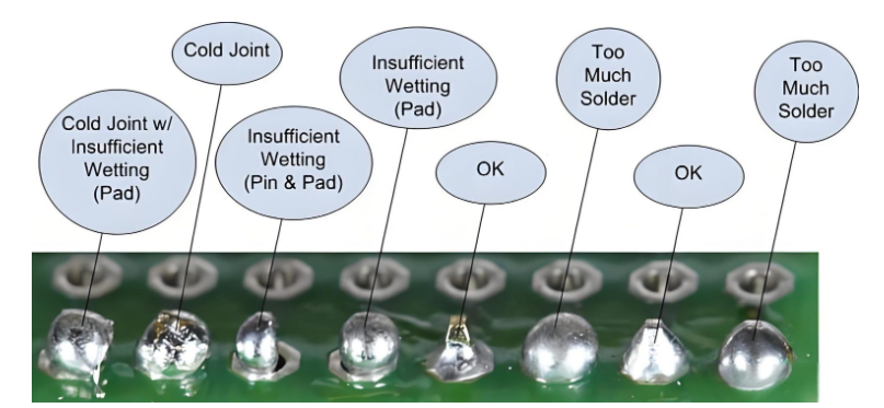
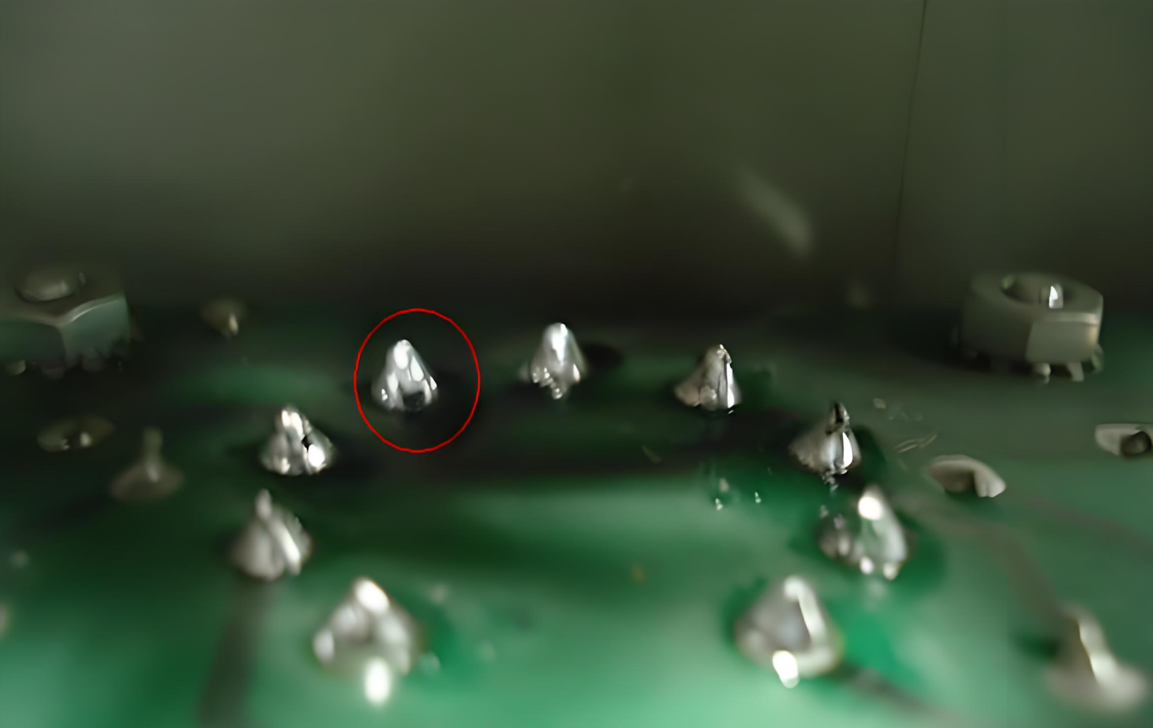
Cold Solder Joint Pictures
Visual aids can be extremely helpful in identifying cold solder joints. Here are common visual signs:
Dull, Grainy Appearance: A good joint is shiny and smooth. Cold ones look frosty or matte.
Cracks or Gaps: Visible separations or voids between the component and pad.
Ball-Like Shape: If the solder beads up instead of flowing smoothly, it likely didn’t bond.
Lifting Leads: Components that seem slightly off the pad may signal a cold joint underneath.
Identifying a good solder joint is just as important as recognizing a cold one. A high-quality solder joint has several distinct characteristics:
1. Appearance
A good solder joint should have a smooth, shiny, and concave surface. The solder should flow evenly around the component lead and onto the PCB pad, forming a natural fillet.
2. Wetting
Proper wetting is a key indicator of a good solder joint. The solder should spread and adhere evenly to both the component lead and the PCB pad, covering the surfaces completely. When the wetting is correct, there will be no gaps, voids, or bare spots where the metal surfaces are exposed.
3. Strength
A well-soldered joint should be strong enough to hold the component in place firmly. Gently tugging on the component (with appropriate care not to damage it) should reveal a solid connection.
How to Avoid Cold Solder Joints?
Prevention is better than repair. Here’s how to keep cold solder joints from happening in the first place:
1. Use the Right Temperature
Always set your soldering iron between 350°C to 400°C for standard lead-based solder. Higher temperatures may be needed for lead-free types.
2. Pre-Clean Pads and Leads
Use isopropyl alcohol to clean surfaces before soldering. Dirt and oxidation are invisible enemies.
3. Don’t Skip the Flux
Flux removes oxidation and improves solder flow. Many solder wires include it, but extra flux helps in difficult spots.
4. Keep Steady Hands
Hold the component and iron steady until the solder cools. Use clamps or tools if needed.
5. Pick Quality Tools
Poor-quality irons with unstable tips lead to inconsistent heat. Invest in a reliable soldering station with temperature control.
6. Work in a Clean, Static-Safe Area
Humidity, static, and poor lighting all raise the chances of making mistakes.
How to Fix Cold Solder Joints?
Despite our best efforts, cold solder joints may still occur. Fortunately, there are ways to fix them:
1. Soldering
The first step in fixing a cold solder joint is often desoldering. Use a desoldering pump or wick to remove the existing solder from the joint. Heat the joint with the soldering iron to remelt the solder, and then use the desoldering tool to suck up or absorb the molten solder. Make sure to remove all the old solder completely to start fresh.
2. Cleaning
After desoldering, clean the surfaces again to remove any flux residues, oxidation, or other contaminants that may have accumulated. This step is crucial for ensuring a proper repair. Use a suitable cleaning solution and a clean brush or cloth to wipe the surfaces clean.
3. Resoldering
Once the surfaces are clean, it’s time to resolder the joint. Apply a small amount of fresh flux to the cleaned surfaces, and then heat the joint with the soldering iron. When the flux starts to bubble and activate, feed a small amount of solder into the joint.
4. Inspection and Testing
After resoldering, inspect the joint visually to make sure it looks good and meets the criteria for a proper solder joint. Then, use testing equipment to verify the electrical connection. Check for continuity and make sure the joint is conducting electricity properly. If any issues are found, repeat the desoldering, cleaning, and resoldering process until the joint is fixed.
Trust PCB Assembly Service Provider – EBest Circuit (Best Technology)
Avoiding cold solder joints isn’t just about skills—it’s also about choosing the right PCB assembly partner. At EBest Circuit (Best Technology), we follow strict quality processes to ensure every joint is clean, strong, and reliable. Here’s how we guarantee excellence:
X-ray and AOI Inspection: We detect hidden cold joints and ensure solid connections throughout.
Skilled Technicians: Our team is trained to international IPC standards, ensuring precision with every solder joint.
Fast Prototyping and Mass Production: Whether you’re scaling up or fine-tuning, we support your project at every stage.
Need flawless assembly for your next project? Contact EBest Circuit (Best Technology) today for a quote or consultation. Let’s build something reliable—together.
FAQs
1. What is a cold solder joint in simple terms?
It’s a weak or poorly connected solder point that didn’t heat properly and can fail over time.
2. Are cold solder joints dangerous?
Yes, they can cause circuits to fail, especially in safety-critical systems like medical or automotive electronics.
3. Can cold solder joints be fixed easily?
Yes, with the right tools, you can reheat and repair them quickly.
4. What does a cold solder joint look like?
It often appears dull, cracked, grainy, or uneven—unlike a shiny, smooth good joint.
5. Can a PCB test miss a cold solder joint?
Yes, especially if the fault is intermittent. That’s why visual inspection and X-ray are important.
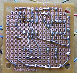
A perf board, often referred to as a perforated board, is a type of printed circuit board (PCB) that’s widely used in prototyping and DIY electronics. Unlike fully fabricated PCBs, a perf board offers a flexible way to mount and wire components before committing to a finalized design. If you’ve ever wondered how electronics hobbyists or engineers test ideas quickly, perf board printed circuit boards (PCBs) are often the answer.
What is Perf Board Printed Circuit Boards PCBs?
Perf boards are thin boards made from an insulating material like fiberglass or phenolic resin, pre-drilled with evenly spaced holes. These holes are laid out in a grid pattern and are designed to hold through-hole electronic components. The term “perf board printed circuit boards PCBs” refers to this category of PCBs that lack pre-designed traces but allow for custom circuit construction.
Unlike standard PCBs, perf boards don’t come with etched copper paths. You can design your own connections using wires or solder bridges, offering full control of your circuit layout.
What is Another Name for a Perfboard?
Perfboards are also known as prototyping boards, dot boards, or project boards. In some circles, they’re casually called “proto boards.” While names vary, their purpose remains the same: to provide a quick, hands-on way to build, test, and modify circuits during the design phase.
What is Perf Board Made Of?
Most perf boards are made from one of two materials:
FR4 (Fiberglass Reinforced Epoxy): Durable and commonly used in professional settings.
Phenolic Resin: More affordable but slightly brittle, usually found in budget DIY kits.
The board has a grid of holes, and in some cases, those holes are surrounded by copper pads, especially in copper-clad perf boards. These pads allow easy soldering of components and jumpers.
What Does a Perf Board Do?
A perf board allows engineers and hobbyists to construct electronic circuits manually. You mount components through the holes and connect them with wire or solder to form the circuit. It’s especially useful for:
Rapid prototyping
Small-scale production
Educational projects
Repair or replacement circuits
Perf boards eliminate the wait time and cost associated with custom PCB fabrication during early design phases.
What is the Difference Between a Perf Board and a Breadboard?
This is a common question for beginners, and the differences are worth understanding:
Feature
Perf Board
Breadboard
Reusability
Single-use
Reusable
Soldering
Required
Not needed
Electrical Conductivity
Manual with wires/solder
Internal metal strips
Component Stability
Permanent
Temporary
Best for
Finalizing prototypes
Initial testing & concept design
If you’re experimenting with a new idea, start with a breadboard. When you’re ready to make it permanent, switch to a perf board.
Perf Board Dimensions
Perf boards come in various standard sizes, typically measured in holes (e.g., 60×40 holes) or in millimeters. Here are a few common options:
3cm x 7cm (30mm x 70mm): Great for small circuits or microcontroller projects
5cm x 7cm: A medium size, popular for Arduino-based designs
9cm x 15cm: Ideal for complex circuits with more components
The standard hole spacing is 2.54mm (0.1 inch), which aligns perfectly with most DIP (dual in-line package) components.
Perf Board Price
Prices vary based on size, material, and copper coverage. Here’s a general range:
Small perf board (3×7 cm): $0.20–$1.00 each
Medium board (5×7 cm): $0.50–$2.00 each
Large board (9×15 cm): $1.50–$5.00 each
Buying in bulk usually reduces cost. For instance, a 10-pack of medium boards may cost under $10 on platforms like Amazon, AliExpress, or Digi-Key.
How to Use a Perf Board?
Using a perf board is an excellent way to build a permanent version of a prototype circuit. Here’s a step-by-step approach to help you get started—even if you’re new to soldering or circuit design:
1. Plan Your Layout
Before inserting components, sketch your circuit on paper or use software like Fritzing or KiCad. Try to place components in a way that minimizes the number of jumpers and crossing wires. Make sure power and ground rails are easy to access.
2. Insert the Components
Place the components into the holes of the perf board with the leads facing down. Start with the shortest components (like resistors), then work your way up to taller ones (like capacitors or IC sockets). This helps keep the board level while soldering.
3. Secure the Components
Bend the leads slightly on the bottom side of the board to hold components in place. This is especially helpful if you’re working with many parts at once or if the board is going to be moved before soldering.
4. Solder the Leads
Once your components are in place, flip the board over and solder each lead to its corresponding pad. Try to heat both the pad and the lead at the same time for a clean solder joint.
5. Trim Excess Leads
After soldering, use flush cutters to snip off the extra length of the component leads. This prevents shorts and makes the back of the board neat.
6. Make Electrical Connections
Now it’s time to connect the components electrically. You can use:
Hook-up wire: Strip and bend it to form paths between solder points.
Solder bridges: Add a small amount of solder to connect two nearby pads.
Insulated jumper wires: For long connections across the board.
Tip: Color-code your wires for easier troubleshooting later (e.g., red for VCC, black for GND, yellow for signal).
7. Test the Circuit
Before powering up, check all connections with a multimeter. Look for continuity and confirm there are no shorts between adjacent traces or leads.
This process may take a bit of time, but it helps you build a functional and clean circuit that’s much more durable than a breadboard setup.
Perfboard Soldering Tips and Techniques
Soldering is a crucial step when working with perf boards. Good soldering makes your circuit reliable and long-lasting. Here are some essential tips and techniques to get better, cleaner, and more efficient solder joints:
1. Use the Right Soldering Iron
Choose a soldering iron with a fine tip and adjustable temperature, especially for delicate components. A temperature of around 350°C is good for most standard soldering jobs.
2. Select Quality Solder
Use 60/40 tin-lead rosin core solder or lead-free solder if safety or regulations require it. Thin solder (like 0.6mm) is easier to control for small connections.
3. Keep the Tip Clean
Clean the soldering iron tip with a damp sponge or brass wire before and after every few joints. This helps maintain heat transfer and reduces oxidation.
4. Pre-tin the Tip
Apply a small amount of solder to the tip before you start. This thin coating improves heat transfer to the pad and component lead.
5. Solder Quickly and Precisely
Touch the iron to the joint (pad and lead) for about 1–2 seconds, then feed in solder. Pull the iron away once enough solder has flowed. Avoid lingering too long, as overheating can damage the pad or component.
6. Avoid Cold Solder Joints
Cold joints happen when the solder doesn’t melt fully. They appear dull or cracked and can lead to unreliable connections. Always ensure the joint is shiny and slightly concave.
7. Use Heat Shrink or Insulation
When making jumpers or exposed connections, cover them with heat shrink tubing or use insulated wire to prevent accidental shorts.
8. Work in a Well-Ventilated Area
Soldering fumes can be harmful. Work near a window or use a small fume extractor to keep the air clean.
9. Double-Check Your Work
After finishing the soldering, inspect every joint. Use a magnifying glass if needed. A continuity check with a multimeter is also recommended.
10. Practice Makes Perfect
If you’re new to soldering, consider practicing on a spare perf board with some scrap components. Developing steady hands and learning how solder flows will improve your technique quickly.
Why Choose EBest Circuit (Best Technology) for Custom PCBs?
While perf boards are great for prototyping, finalized products need custom-made PCBs. That’s where EBest Circuit (Best Technology) comes in. We specialize in designing and manufacturing high-quality PCBs for various industries, from consumer electronics to automotive and aerospace.
We use a MES traceability system, provide professional engineering support, and offer competitive pricing even for low-volume orders. Whether you’re upgrading from perf board to custom PCB or need help bringing a prototype to life, EBest Circuit (Best Technology) has you covered.
FAQs
1. Can I use surface-mount components on a perf board?
Yes, but it’s trickier. You’ll need to manually create pads using wire or copper tape.
2. Are there perf boards with pre-connected tracks?
Yes, stripboards have rows of connected holes, which help speed up certain circuit designs.
3. Can perf boards handle high current?
Only to a certain extent. For higher currents, wider copper traces or bus bars are preferred.
4. Where can I buy perf boards?
They’re available online on Amazon, eBay, Digi-Key, Mouser, and local electronics stores.
5. What’s the best way to plan a circuit on a perf board?
Use grid paper or software like Fritzing to lay out components before building.
In high-power electronics, thermal management is everything. Whether you’re designing LED modules, motor controllers, or power converters, one of the first decisions you’ll make is selecting the right copper thickness for your copper core PCB.
It’s tempting to assume that more copper is always better. After all, thicker copper offers lower resistance and better heat conduction. But here’s the truth: while thicker copper can enhance performance, it also introduces new challenges—in cost, manufacturability, and even thermal efficiency in certain contexts.
In this article, we’ll dive into how copper thickness affects heat dissipation, mechanical integrity, and overall PCB performance. You’ll also learn how to find the sweet spot—balancing copper thickness with practical requirements.
What Does Copper Thickness Really Do in a PCB?
Copper thickness in a PCB is typically measured in ounces (oz), where 1 oz equates to approximately 35 micrometers of thickness. The thicker the copper, the more current it can carry and the more heat it can dissipate—up to a point.
For example:
1 oz copper is standard in many applications like consumer electronics or low-power LED boards.
2 oz–3 oz copper is often used in medium- to high-power applications, such as telecom equipment or automotive control modules.
4 oz–6 oz copper or more is reserved for ultra-high-current or extreme thermal environments, like industrial drives or inverters.
In a copper core PCB, the copper layer not only serves as a trace but also acts as a heat conduit. But simply adding more copper isn’t always the best strategy—it needs to be balanced with mechanical, thermal, and design constraints.
How Does Thicker Copper Affect Thermal Conductivity?
Thermal conductivity is the rate at which heat passes through a material. Copper’s thermal conductivity is excellent—about 398 W/m·K—much higher than FR4 (0.25 W/m·K) or aluminum (205 W/m·K). Thermal conductivity improves as copper gets thicker—up to a point.
A 1 oz (35µm) copper layer offers good heat flow for standard loads.
2 oz (70µm) or 3 oz (105µm) copper layers are used for medium-to-high power circuits.
Ultra-thick copper like 6 oz (210µm) or more is suitable for extreme applications like power inverters or motor drivers.
But while thicker copper improves thermal conductivity, it also increases thermal mass, which can slow down heat transfer in fast-cycling circuits. That means copper core PCBs with ultra-thick copper aren’t always the most efficient in dynamic thermal environments.
What Happens to Mechanical Strength as Copper Gets Thicker?
A copper core PCB with heavy copper also becomes more rigid. This can be beneficial in harsh environments (e.g. EV chargers, industrial robots) where vibration or mechanical shock is a concern.
However, ultra-thick copper comes with drawbacks:
Reduced flexibility: Too much copper can crack during mechanical stress.
Higher internal stress: Thicker copper can warp other layers if not carefully designed.
Drilling and routing challenges: High copper thickness limits hole aspect ratio and increases the risk of burrs or tool breakage.
In short, thicker copper increases strength but decreases the PCB’s resilience during assembly or use.
Manufacturing Challenges of Thick Copper Core PCBs
As copper thickness increases, so does the cost—not just of materials, but also in processing:
Etching Control: The deeper the copper, the harder it is to maintain precise trace widths and spacing. Over-etching or under-etching can occur, especially with high-aspect-ratio designs.
Drilling Difficulties: Thick copper increases drill wear and may require specialized bits. This adds time and cost.
Solder Mask Issues: Solder mask adhesion becomes less reliable with thick copper due to surface tension and lack of anchor points.
Fine-pitch traces are harder to produce with heavy copper.
A copper core PCB with 3 oz copper may cost up to 1.8x more than a standard 1 oz version. And a 6 oz copper design might require specialized etching equipment, which not all PCB manufacturers can support. That’s why working with an experienced supplier like EBest Circuit (Best Technology) is crucial.
How to Choose the Right Copper Thickness for Your PCB?
Rather than defaulting to the thickest copper available, consider these design factors:
Power Dissipation
Estimate total wattage and heat output. Use simulation tools or thermal imaging to understand hot zones.
Current Capacity
Follow IPC-2152 guidelines to determine trace width vs. amp load. For example:
1 oz copper: ~10A for 100 mil trace (surface)
2 oz copper: ~18A for same width
Board Size and Layer Count
Larger boards may use thinner copper with thermal vias and heat sinks. Multilayer designs must balance all layers.
Application Environment
Will the board be exposed to vibration, moisture, or rapid temperature swings? If yes, go thicker and stronger.
Budget and Lead Time
Thick copper PCBs cost more and take longer to fabricate. Optimize design for performance within your price range.
Rule of thumb:
Use 1 oz–2 oz copper for LED lighting, chargers, and automotive control boards.
Go for 3 oz–4 oz only if you have continuous high current or extreme heat.
Consider 5 oz+ only for industrial power systems or heavy-duty applications.
Case Study: How Thicker Copper Solved and Created Problems
A client building a 500W motor driver switched from 2 oz to 5 oz copper core PCB to improve thermal dissipation. While heat decreased by 12%, they faced new issues:
Via drilling became inconsistent due to copper pull-out.
Board warpage increased after reflow soldering.
Assembly cost rose by 30%.
We helped them optimize with a hybrid solution:
Kept 2 oz on signal layers.
Added localized copper in power zones.
Improved base layer contact for better heat flow.
Finally, thermal performance remained strong, but manufacturability and cost were brought back under control.
Conclusion
When designing a copper core PCB, it’s easy to fall into the trap of thinking “thicker is better.” In reality, optimal performance comes from careful engineering—not just stacking on copper.
At EBest Circuit (Best Technology), we help clients worldwide balance copper thickness with thermal, mechanical, and manufacturing constraints. We use simulation, prototype validation, and DFM support to ensure your final product is both high-performing and cost-effective.
Why Work With EBest Circuit (Best Technology) for Copper Core PCBs?
✔️ IPC-compliant thermal and electrical simulations
✔️ MES-based quality traceability
✔️ Rapid prototyping and scalable mass production
We help you avoid over-designing or under-designing copper thickness—saving cost and ensuring long-term reliability. No matter the application—EVs, LEDs, telecom, or industrial—you’ll find the right copper balance with us.
Call To Action
Want to know more information about copper base PCB?
In our last blog, we introduced the definition and basic of copper core PCB. But copper core PCB isn’t the only one metal core PCB, aluminum PCB provides good heat dissipation as well. So, when working with metal core boards, many engineers and buyers are unsure whether to choose an aluminum PCB or a copper core PCB. Some believe copper is always better, while others go with aluminum for lower cost. Today, we will guide you how to choose them, then let’s start it!
Material Comparison: Copper vs Aluminum Core
Both copper and aluminum are used as the core material for thermal management in PCBs, but their physical and electrical properties differ significantly:
Property
Copper
Aluminum
Thermal Conductivity
~380–400 W/m·K
~200–230 W/m·K
Electrical Conductivity
~58 MS/m
~35 MS/m
Density
8.96 g/cm³
2.70 g/cm³
Strength
Higher rigidity
More flexible
Cost
1.5x to 3x higher
Lower
Copper provides superior conductivity and better rigidity but comes at a much higher cost and weight. Aluminum is lighter, easier to machine, and cost-effective for mid-range applications.
Thermal Management: Which One Handles Heat Better?
When heat dissipation is your top priority, copper clearly wins. Its high thermal conductivity allows heat to spread faster and more evenly, which is critical in high-power applications like:
LED floodlights and stadium lighting
Automotive headlights
Power converters and inverters
Laser driver modules
Case example: A customer replaced an aluminum PCB with a copper base for a 100W LED driver. The operating temperature dropped by 15°C, drastically improving product lifespan.
However, in low-to-mid power systems—like ceiling lights, LED bulbs, or camera light rings—aluminum is typically sufficient. Using copper in these cases is often unnecessary and drives up costs without clear benefits.
Mechanical Strength and Weight: What Does Your Design Need?
Copper core PCBs are heavier and more rigid, which makes them better for industrial applications exposed to vibration or extreme temperature cycles.
But in products where weight matters—like drones or wearable devices—aluminum PCBs are the smarter option. They are easier to machine, route, and assemble. They also cost less in terms of tooling and manufacturing time.
Choose copper core PCBs if you need:
High mechanical stability
Vibration resistance
Long-term thermal durability
Choose aluminum PCBs if your product needs:
Lightweight design
Cost control
Simpler routing and drilling
Cost Consideration: Is Copper Always Worth It?
Let’s be honest: copper core PCBs can cost up to 3x more than aluminum PCBs. So you should ask yourself—is the higher thermal performance really necessary for your design?
Aluminum PCBs are the better choice when:
Your application doesn’t exceed 80W–100W
Weight and cost are design priorities
You’re in mass production and need price stability
Copper core PCBs are justified when:
Your system needs to handle heavy heat loads
High current density is involved
Long-term reliability matters more than price
Many of our customers reduce total project cost by switching to aluminum PCBs without sacrificing performance—once we review their thermal simulation data.
Where to Use Each PCB Type?
Here’s a quick-reference table to match your application with the recommended base material:
Application
Recommended Base
Reason
High-power LED floodlights
Copper
Heat and current requirements are high
Automotive lighting systems
Copper or thick aluminum
Performance and safety critical
Indoor LED lighting
Aluminum
Lower heat, cost-sensitive
Power modules & inverters
Copper
High voltage and thermal stress
Camera flash or ring light
Aluminum
Lightweight and cost-friendly
Medical power supply
Copper
Stability and safety required
LED floodlights (150W+)
Copper Core PCB
Handles heat better
LED bulbs & home lighting
Aluminum PCB
Affordable and thermally sufficient
EV chargers & power modules
Copper Core PCB
High reliability under load
Camera flashes & portable lights
Aluminum PCB
Lightweight and budget-friendly
Medical devices (power control)
Copper Core PCB
Precise, stable performance
Consumer electronics
Aluminum PCB
Cost-efficient for large volumes
Use this guide to avoid over-engineering or under-specifying your metal core PCB.
5 Key Points Before You Choose
Still not sure which base material fits your needs? Walk through this five-step checklist:
1. Power Level: How much current and heat does your circuit handle?
2. Installation Environment: Is weight a constraint? Will it face vibration?
3. Target Cost: Are you selling a premium or mass-market product?
4. Design Complexity: Do you need tight tolerances or complex routing?
5. Volume & Lead Time: Can your supplier meet deadlines for the material?
If you answered “high” for performance on most points, copper is likely the way to go. If not, aluminum is your best cost-performance choice. By the way, if you’re unsure after answering these, consult with your PCB manufacturer. At EBest Circuit (Best Technology), we provide application-based advice to help you choose between aluminum PCBs and copper core PCBs—without overspending.
Why Choose EBest Circuit (Best Technology) for Your Metal Core PCB?
Whether you need aluminum base PCBs for standard lighting or copper base PCBs for high-power industrial applications, EBest Circuit (Best Technology) has you covered:
Mature production lines for both copper and aluminum base PCBs
One-on-one design support, thermal simulation, and DFM reviews
Full in-house capabilities: thick copper etching, CNC routing, V-cutting
Fast sample turnaround and stable mass production support
Strict quality control and traceability through MES system
Expert engineering team for application-specific advice
Reach out to EBest Circuit (Best Technology)—we’ll help you analyze your application, recommend the ideal PCB solution, and even support custom development if needed.
FAQs
Q1: Can I use aluminum base PCBs for high-power applications?
Only for moderate heat loads. For >100W power systems, copper is strongly recommended.
Q2: What is the thinnest aluminum or copper base you can provide?
We can produce down to 0.8mm base thickness for both, depending on the structure.
Q3: Do you offer hybrid metal core PCBs?
Yes, we can integrate aluminum and FR4 or support copper-ceramic hybrid designs.
Q4: How long is the lead time for copper vs aluminum base?
Aluminum PCBs: 5–7 working days; Copper PCBs: 7–12 days depending on complexity.
Q5: Can I get thermal simulation before placing an order?
Absolutely! We offer pre-production thermal analysis and structural design assistance.
Q6: Are copper core PCBs compatible with standard SMT processes?
Yes, they are. We offer full SMT assembly services for both aluminum and copper base boards.
Q7: How do I know which type is best for my application?
Send us your design or specs, and we’ll recommend the most cost-effective and reliable option.
Conclusion
Choosing between a copper core PCB and an aluminum PCB isn’t about choosing the better material. It’s about selecting what’s right for your application. Copper is powerful but expensive; aluminum is flexible and affordable.
When designed and selected correctly, aluminum PCBs can outperform expectations, and copper core PCBs can save your system from thermal failure. Match the material to your environment, budget, and performance goals—and you’ll never go wrong. In our next blog, we will share how to select the thickness of copper. If you are interested in it, collect us and keep reading.
Copper base PCBs have become increasingly popular in high-power and thermally demanding applications. But many customers still ask: “Is it really suitable for my project?” If you’re in LED lighting, power electronics, automotive, or any field requiring excellent heat dissipation, this article is for you. We’ll walk you through what copper base PCBs are, their key advantages, and how to determine whether they’re the right fit for your product.
What Is a Copper Base PCB?
A Copper Base PCB is a type of metal core printed circuit board (MCPCB) that uses copper as the base material instead of the more common aluminum or FR4. This type of board is specifically designed to handle high heat, high power, and mechanical stress. The copper base acts as a heat sink, pulling heat away from components and distributing it more evenly. Compared with FR4 PCB, copper PCBs offer superior heat conductivity, mechanical strength, and current-carrying capacity.
Typical Structure of a Copper Base PCB
The structure of a copper base PCB is generally composed of three main layers, each playing a critical role in the board’s performance:
Copper Circuit Layer (Top Layer):
This layer contains the etched copper traces that form the electrical pathways. In copper base PCBs, this layer is often thicker than in standard PCBs—ranging from 1 oz to 20 oz or more—to handle higher current loads and improve heat distribution. These traces can be plated or coated depending on the application or customers requirements (e.g., ENIG, HASL, OSP).
Thermal Dielectric Layer (Middle Layer):
This is the insulating layer between the circuit and the metal base. It’s designed to have high thermal conductivity and excellent electrical insulation. Its main function is to transfer heat from the components to the copper base below while keeping the circuits electrically isolated. The thermal conductivity of this layer often ranges from 1 W/m·K to over 10 W/m·K, depending on material choice.
Copper Base Layer (Bottom Layer):
Unlike typical MCPCBs that use aluminum, this layer is made of solid copper—usually ranging from 1 mm to 3.5 mm thick or more. This acts as a heat sink, pulling heat away from the circuit layer and rapidly dispersing it. Copper’s thermal conductivity is about 400 W/m·K, significantly higher than aluminum (~200 W/m·K).
This design structure enables heat to be quickly conducted from the components to the copper baseplate, and then transferred through the heat sink or the casing, thereby enhancing the overall thermal management capability of the system.
What Are the Core Advantages of Copper Base PCBs?
Clients often wonder: “Why should I pay more for a copper base board?” Here’s why it might be worth it:
Exceptional thermal conductivity – Copper is far more effective at dissipating heat than aluminum or FR4, very suitable for high-wattage components.
High current tolerance – With thicker copper layers, these PCBs handle larger currents with minimal resistance.
Excellent mechanical durability – Copper PCBs are stronger and can withstand physical stress, vibration, and temperature cycling.
Improved electromagnetic shielding – Their dense base helps suppress EMI, a critical benefit in high-frequency applications.
These benefits result in longer product life, more consistent performance, and fewer field failures, especially in mission-critical applications.
Which Industries Benefit Most from Copper Base PCBs?
LED Lighting – High-power LEDs like COB, UV LED, floodlights, and grow lights require efficient thermal management.
Power Electronics – Power supplies, inverters, and converters benefit from copper’s high current-carrying capacity.
Automotive – EV batteries, headlights, and control systems need durability and consistent heat dissipation.
Telecom & RF Devices – Copper PCBs handle high frequencies with reduced signal loss and better EMI shielding.
Medical Equipment – High reliability is key for precision instruments that cannot afford overheating.
If your product involves heat, high power, or harsh environments, copper base PCBs are often the most dependable choice.
How Can You Tell If a Copper Base PCB Is Right for Your Project?
Before committing, ask yourself the following:
1. Does your design generate significant heat?
2. Is there limited space, but high power density?
3. Are you struggling with product reliability or failures due to overheating?
4. Is your end-product used in mission-critical or high-reliability environments?
If you answered “yes” to two or more of these, a copper base PCB could greatly improve your performance and reliability.
What Are the Limitations or Considerations of Copper Base PCBs?
While copper base PCBs offer outstanding thermal and electrical performance, they are not suitable for every project. Understanding their limitations and key design considerations is essential to avoid overdesign, unnecessary costs, or compatibility issues in your application.
1. Higher Material and Production Cost
Copper is significantly more expensive than aluminum or fiberglass (FR4). This cost factor affects both raw material pricing and manufacturing expenses. Additionally, the thicker copper layers and heavier base not only cost more to source, but they also require more energy and effort to process, increasing the total cost of production.
2. Heavier Board Weight
Copper has a high density (8.96 g/cm³ compared to aluminum’s 2.70 g/cm³), which means copper base PCBs are substantially heavier. This can present challenges in:
Weight-sensitive products such as drones or handheld devices
Shipping and logistics costs, especially for large quantities
Mechanical handling in assembly lines
Tip: If you’re designing a compact or mobile device, consider whether the weight trade-off justifies the thermal benefit.
3. More Challenging to Fabricate and Process
Due to the hardness and thickness of the copper base, special tooling, slower machining speeds, and experienced operators are required. Fabricators must use tougher drill bits, precise CNC machines, and advanced lamination processes to ensure:
Clean drill holes
Accurate etching and layering
Strong adhesion between layers
Poor processing can result in delamination, cracks, or electrical leakage—especially at the dielectric interface.
4. Limited Flexibility in Complex Layer Stack-Ups
While single-layer copper PCBs are common, multi-layer copper base PCBs are difficult and expensive to produce. This is because:
Each additional layer increases complexity in lamination
Heat must still flow effectively through the stack
Alignment and insulation tolerance become more critical
Not all manufacturers offer multi-layer copper PCBs due to the strict processing requirements and lower production yields.
5. Thermal Expansion and Stress Considerations
Copper has a relatively low coefficient of thermal expansion (CTE), which is good for dimensional stability. However, when paired with dielectric materials or mounted in assemblies with mismatched CTEs, thermal stress can build up during repeated heating and cooling cycles.
This can lead to:
Micro-cracking
Solder joint fatigue
Mechanical warping of the board
If you need help evaluating whether copper base PCBs are the right choice for your next project, EBest Circuit (Best Technology)’s engineering team is here to offer thermal simulation, design review, and cost-performance optimization—so you only pay for what you truly need.
Why Choose EBest Circuit (Best Technology) for Your Copper Base PCBs?
When it comes to copper base PCBs, expertise matters. At EBest Circuit (Best Technology), we provide end-to-end solutions — from thermal simulation and material selection to rapid prototyping and mass production.
Why choose us?
✅ One-on-one engineering support
✅ In-house thermal and mechanical design assistance