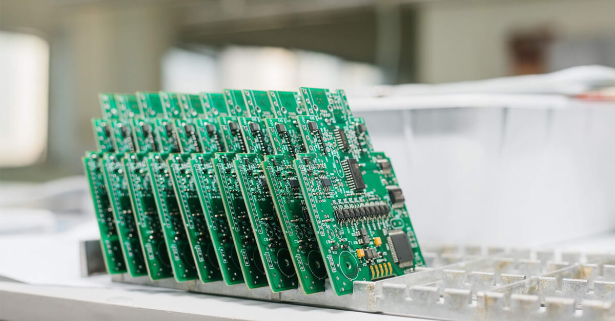
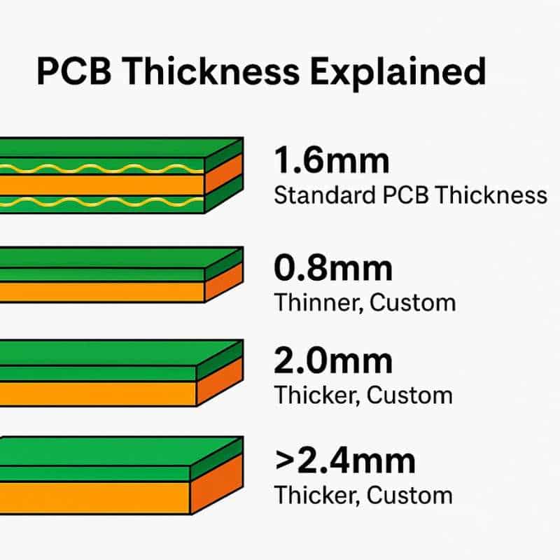
The standard PCB thickness is 1.6 mm (0.063 inch). This thickness has become the global default because it balances mechanical strength, electrical reliability, manufacturability, and cost. Most PCB fabs optimize their processes, materials, and tooling around 1.6 mm, making it the most economical and widely supported option.
What Are Standard PCB Thicknesses?
Standard PCB thicknesses are the most commonly produced finished board thickness values supported by mainstream fabrication lines. These values exist because materials, lamination presses, drilling tools, and surface finish processes are optimized around them.
For rigid boards, the most widely used finished thickness is 1.6 mm. This value has become the industry baseline. It offers a strong balance between rigidity, weight, and cost. Most connectors, card slots, and housings are designed with this thickness in mind.
Other standard thicknesses are also widely used:
- 0.4 mm
- 0.6 mm
- 0.8 mm
- 1.0 mm
- 1.2 mm
- 1.6 mm
- 2.0 mm
- 2.4 mm
These values are not arbitrary. They align with standard FR4 core thicknesses and prepreg build-ups.
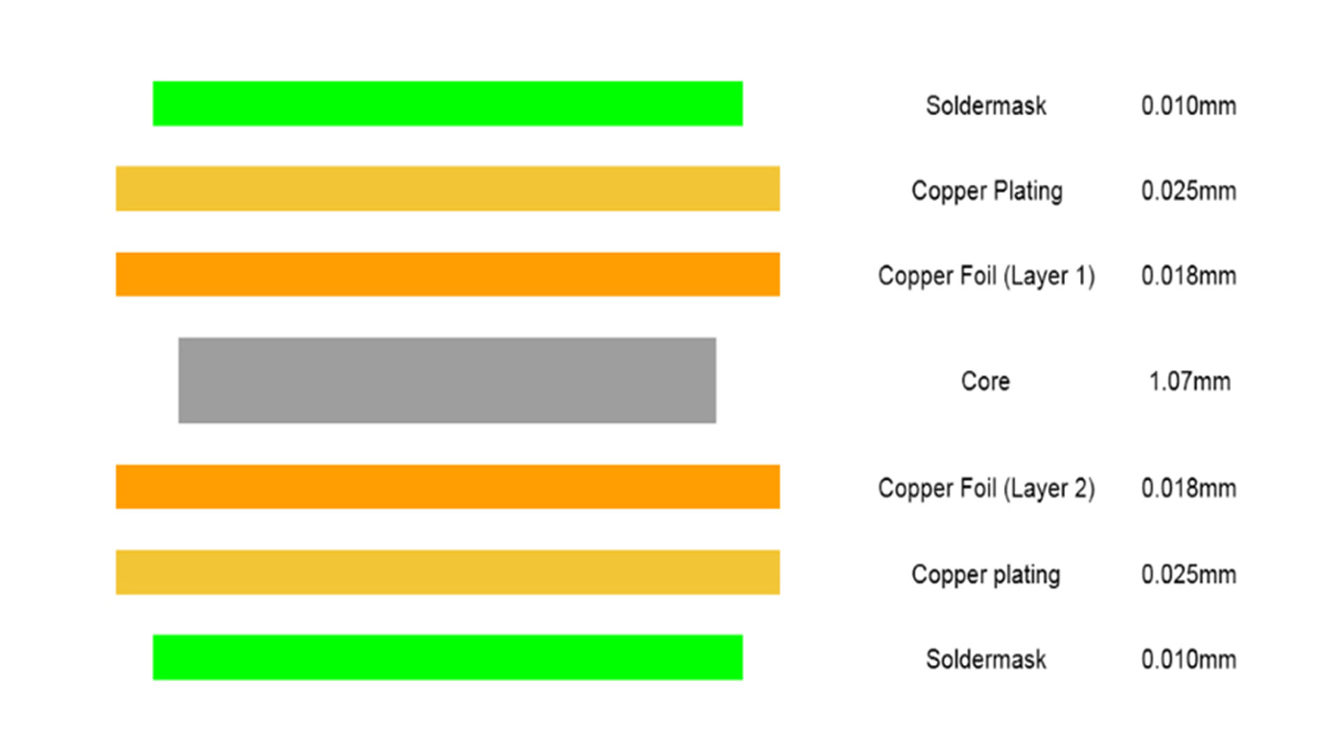
For multilayer boards, the finished thickness results from stacking multiple cores and prepregs. A standard PCB thickness 4 layer design often ends up between 1.2 mm and 1.6 mm, depending on copper weight and dielectric choice.
Because these thicknesses are repeatable, they reduce process variation. That stability is one reason they remain dominant across consumer, industrial, and medical electronics.
Does PCB Thickness Matter?
PCB thickness is very important. It affects performance, assembly, and long-term reliability. A thicker board offers higher rigidity. This reduces flexing during handling and assembly. It also improves resistance to vibration in industrial environments.
- A thinner board saves weight and space. This is valuable in compact products such as wearables or handheld devices. Thin boards also enable tighter stacking in multi-board assemblies.
- Electrically, thickness influences impedance. Controlled impedance traces rely on precise dielectric spacing. Changing thickness without recalculating stack-up can shift impedance out of tolerance.
- Thermally, thicker boards can dissipate heat more evenly. However, very thick boards may trap heat if copper distribution is poor.
In short, PCB thickness matters because it touches mechanics, electronics, and manufacturing at the same time.
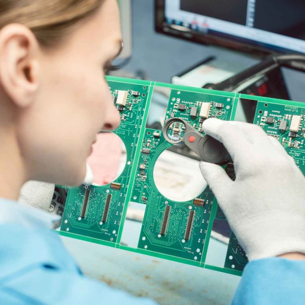
How to Find PCB Thickness?
Finding PCB thickness is straightforward when documentation is available. Most fabrication drawings specify finished thickness in millimeters. Gerber files alone do not define thickness, so you must check the fabrication notes or stack-up table.
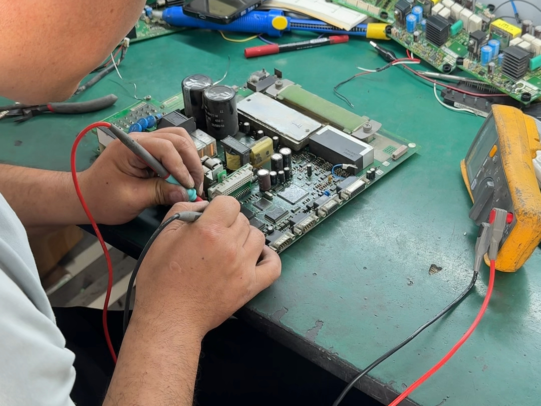
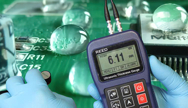
If you already have a physical board, thickness can be measured using a digital caliper. Measure at the edge, away from copper pours or surface finish buildup.
In production environments, thickness is verified during quality inspection. Fabricators use calibrated gauges to ensure boards fall within PCB thickness standard tolerances.
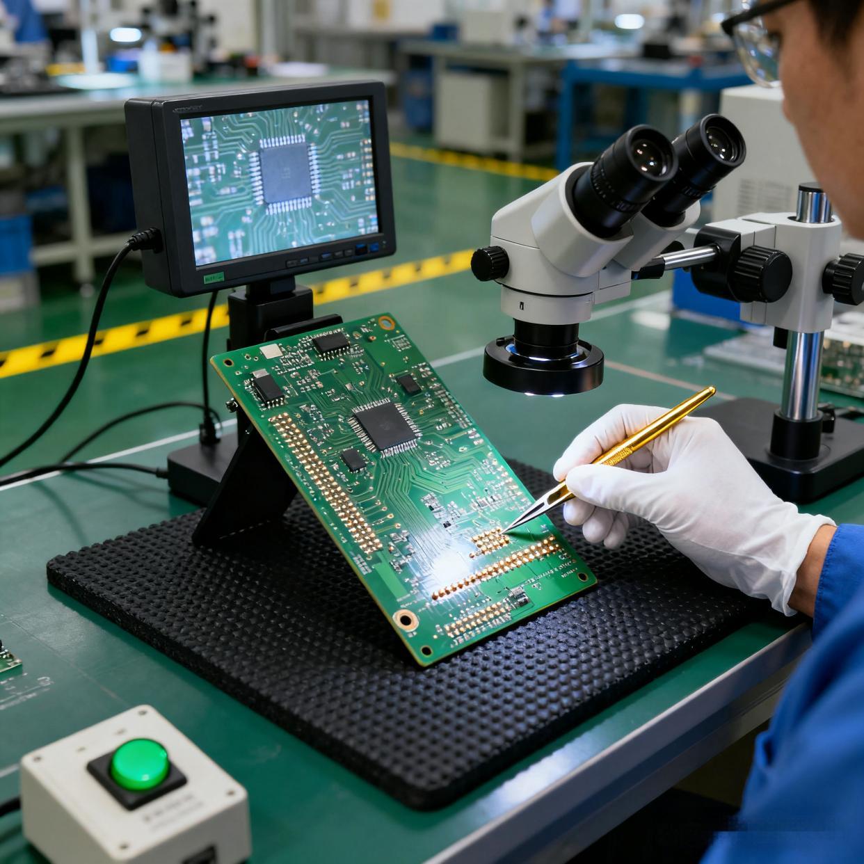
For legacy designs without clear records, cross-section analysis can reveal core and prepreg structure. This method is more involved but provides precise data.
What Is the Standard Thickness of a 2 Layer PCB?
The standard thickness of a 2 layer PCB is most commonly 1.6 mm. This configuration dominates simple control boards, power boards, and general electronics.
Other popular options include:
- 1.0 mm for lighter, space-saving designs
- 0.8 mm for compact modules
- 2.0 mm for higher rigidity
A 2-layer board typically uses a single FR4 core with copper laminated on both sides. Because the structure is simple, thickness control is very stable.
Many designers choose 1.6 mm by default. It fits most connectors and mechanical fixtures. It also minimizes cost because suppliers stock it in large volumes.
What Is the Standard Thickness of FR4 PCB?
FR4 is the most widely used PCB material. Its standard PCB thickness options match the common rigid board values.
Typical FR4 finished thicknesses include:
- 0.8 mm
- 1.0 mm
- 1.2 mm
- 1.6 mm
- 2.0 mm
The internal standard PCB core thicknesses are smaller. Common FR4 core thicknesses are:
- 0.1 mm
- 0.2 mm
- 0.3 mm
- 0.4 mm
By combining these cores with prepreg layers, fabricators achieve the final board thickness. Copper weight also plays a role. Heavy copper adds measurable thickness, especially in multilayer designs.
FR4 remains popular because it offers good electrical insulation, stable mechanical properties, and reasonable cost. Its standard thickness range supports almost every general application.
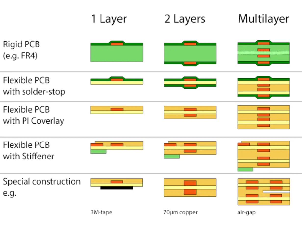
How Thick Is a Standard Flex PCB?
Flex PCBs follow different rules. Their thickness is much thinner because flexibility is the goal.
A standard flex PCB thickness often ranges from 0.05 mm to 0.3 mm, depending on layer count and stiffener use. Single-layer flex circuits are extremely thin. They use polyimide substrates rather than FR4.
Double-layer and multilayer flex boards add thickness but remain far thinner than rigid boards. Adhesives, coverlay, and copper weight all contribute to the final value.
When stiffeners are added, the thickness increases locally. This allows connectors to be mounted without sacrificing flexibility elsewhere.
Flex thickness must be chosen carefully. Too thin, and handling becomes difficult. Too thick, and flexibility is reduced.
How to Choose the Thickness of PCB?
Choosing PCB thickness should start with the application, not habit. While standard values simplify sourcing, the best thickness depends on real constraints.
- First, consider mechanical requirements. Boards exposed to vibration or stress benefit from greater thickness. Boards mounted in tight enclosures may need to be thinner.
- Next, review electrical needs. High-speed designs rely on precise impedance. Thickness affects dielectric spacing, so it must align with the stack-up calculation.
- Thermal performance also matters. Power boards may need thicker substrates or heavier copper to spread heat.
- Assembly is another factor. Thin boards can warp during reflow if not supported properly. Thicker boards resist warpage but increase weight.
- Finally, cost and lead time matter. Standard thicknesses are faster and cheaper. Custom thicknesses may require special materials.
What Is the Standard Thickness Tolerance for PCB?
No PCB is perfectly uniform. Every board is produced within a tolerance range. Standard PCB thickness tolerance depends on board type and thickness.
For rigid FR4 boards, a typical tolerance is ±10% of the finished thickness. For a 1.6 mm board, this means a range of approximately 1.44 mm to 1.76 mm.
Thinner boards often have tighter absolute tolerances but similar percentage limits. Multilayer boards may show slightly more variation due to multiple lamination steps.
What Is the Minimum Core Thickness of a PCB?
The minimum PCB thickness is limited by core material availability and handling constraints. In rigid boards, standard FR4 cores rarely go below 0.1 mm.
Ultra-thin cores exist, but they increase cost and risk. Thin cores are more fragile during drilling and lamination. They also increase the chance of warp.
In multilayer designs, thin cores are sometimes used to control impedance. This must be balanced against manufacturing yield.
For most applications, using standard core thicknesses improves reliability. It also shortens lead time because materials are readily available.
What Is the Most Common Size PCB?
Standard PCB sizes vary widely because board outlines depend on product design. There is no single universal size. However, certain dimensions appear frequently.
Small control boards often fall within 100 mm × 100 mm. This size is popular because it fits standard fabrication panels efficiently.
Larger boards are common in power supplies and industrial systems. Rectangular shapes dominate because they panelize well.
When discussing standard PCB board sizes, panel utilization matters more than absolute dimensions. Designing with panel efficiency in mind can reduce cost without changing functionality.
Conclusion:
PCB standard thicknesses are the foundation of reliable board design. Thickness influences mechanics, electrical performance, thermal behavior, and manufacturing yield.
If you need guidance on selecting the right standard PCB thickness, material stack-up, or tolerance for your project, our engineering team is ready to support you. Contact us: Email: sales@bestpcbs.com