In the realm of modern electronics, effective thermal management has become a critical factor in ensuring the performance and longevity of devices. As power density in electronic components continues to increase, the need for efficient heat dissipation mechanisms has never been more pronounced. Among the various solutions available, ceramic heat sinks have emerged as a viable and effective option due to their unique properties. This article provides a comprehensive analysis of the applications, advantages, challenges, and future trends of ceramic heat sinks.
Understanding Ceramic Heat Sinks
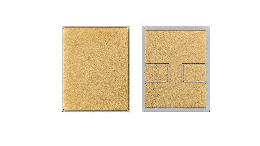
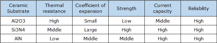
Ceramic heat sinks are thermal management devices designed to absorb and dissipate heat generated by electronic components. They are primarily made from materials such as aluminum oxide (Al2O3), silicon carbide (SiC), and other advanced ceramics. These materials exhibit excellent thermal conductivity and stability at high temperatures, making them suitable for various electronic applications.
Applications of Ceramic Heat Sinks
1. Power Electronics
Ceramic heat sinks are widely used in power electronics, such as inverters and converters. These devices generate significant amounts of heat during operation, and ceramic heat sinks play a crucial role in dissipating this heat to maintain optimal performance and reliability. Their ability to withstand high temperatures makes them ideal for high-power applications, including electric vehicles and renewable energy systems.
2. LED Technology
The use of LED lighting has surged in recent years, and efficient thermal management is essential to maintain brightness and extend the lifespan of LED components. Ceramic heat sinks are increasingly employed in LED applications due to their high thermal conductivity and ability to manage heat effectively. By dissipating heat efficiently, ceramic heat sinks help maintain stable light output and prolong the operational life of LED lighting systems.
3. Telecommunications
In telecommunications, devices such as base stations and routers often operate under heavy loads, generating substantial heat. Ceramic heat sinks are commonly used in these applications to manage thermal loads effectively, ensuring that devices operate within specified temperature ranges. This thermal management is critical for maintaining signal integrity and overall system performance.
4. Aerospace and Defense
The aerospace and defense industries require components that can perform reliably under extreme conditions. Ceramic heat sinks are utilized in various applications, including avionics and satellite systems, where high temperatures and harsh environments are common. Their lightweight and high-temperature resistance make them suitable for applications in aircraft electronics and military equipment, ensuring reliability and safety.
5. Medical Devices
Medical equipment, particularly imaging systems and laser devices, require effective thermal management to ensure safe and reliable operation. Ceramic heat sinks are employed in these applications to dissipate heat generated during operation, preventing overheating and ensuring consistent performance. By maintaining optimal temperatures, ceramic heat sinks contribute to the safety and effectiveness of medical devices.
Advantages of Ceramic Heat Sinks
1. Excellent Thermal Conductivity
Ceramic materials such as aluminum oxide and silicon carbide exhibit high thermal conductivity, allowing ceramic heat sinks to absorb and dissipate heat efficiently. This property is crucial for maintaining optimal operating temperatures in electronic components.
2. High-Temperature Resistance
Ceramics can withstand high temperatures without degrading, making them suitable for high-power and high-frequency applications. This capability ensures that ceramic heat sinks can operate effectively even in extreme conditions.
3. Electrical Insulation
Ceramic heat sinks provide excellent electrical insulation, preventing unwanted current flow between electronic components. This characteristic is essential for applications where electrical isolation is critical to avoid short circuits and enhance safety.
4. Lightweight and Compact Design
Ceramic materials can be engineered to be lightweight, which is beneficial in applications where weight is a concern, such as aerospace and portable electronics. Their compact design also allows for flexible integration into various systems, accommodating space constraints.
5. Corrosion Resistance
Ceramic materials are inherently resistant to corrosion and chemical damage, making them suitable for harsh environments. This property ensures longevity and reliability in applications exposed to corrosive substances.
Challenges of Ceramic Heat Sinks
Despite their advantages, the implementation of ceramic heat sinks comes with challenges.
1. Brittleness
One of the primary challenges of ceramic materials is their brittleness. While they offer excellent thermal performance, they can be susceptible to cracking or breaking under mechanical stress. This brittleness necessitates careful handling during manufacturing and installation.
2. Manufacturing Complexity
The production of ceramic heat sinks can be more complex than that of traditional metal heat sinks. The processes involved, such as sintering and shaping, may require specialized equipment and techniques, increasing manufacturing costs.
3. Cost Considerations
Ceramic materials can be more expensive than metals like aluminum or copper. The higher initial costs may deter some manufacturers, especially in cost-sensitive applications. This financial consideration can limit the broader adoption of ceramic heat sinks in certain markets.
4. Thermal Interface Materials (TIM)
The performance of ceramic heat sinks heavily relies on the quality of thermal interface materials (TIMs) used between the heat sink and electronic components. Selecting the right TIM is crucial for optimizing thermal conductivity, but it can also add to the overall cost and complexity of the assembly process.
Future Trends in Ceramic Heat Sink Technology
The future of ceramic heat sinks looks promising, driven by ongoing research and technological advancements. Several trends are shaping their development.
1. Advanced Material Development
Research into new ceramic materials with enhanced thermal and mechanical properties is ongoing. Innovations in material science could lead to the development of ceramics that combine high thermal conductivity with improved strength and ductility, addressing some of the current limitations.
2. Integration with Active Cooling Solutions
While ceramic heat sinks are predominantly passive cooling solutions, integrating them with active cooling systems—such as fans or liquid cooling—could enhance thermal management capabilities. This hybrid approach may provide greater efficiency in high-performance applications where heat generation is significant.
3. Sustainability and Eco-Friendly Practices
As environmental concerns grow, the development of eco-friendly materials and sustainable manufacturing practices for ceramic heat sinks is becoming increasingly important. This trend will likely influence future designs and production processes.
4. Miniaturization
The continued trend toward miniaturization in electronics demands compact and efficient thermal management solutions. Ceramic heat sinks can be designed to fit into smaller spaces while maintaining effective heat dissipation, meeting the needs of next-generation portable devices.
Conclusion
Ceramic heat sinks play a vital role in the thermal management of modern electronic devices. Their unique properties—such as high thermal conductivity, temperature resistance, and electrical insulation—make them ideal for a wide range of applications, from power electronics to medical devices. While challenges such as brittleness and manufacturing complexity exist, ongoing advancements in materials and techniques are likely to enhance their performance and applicability.
As the demand for high-performance electronics continues to grow, the importance of ceramic heat sinks in effective thermal management will only increase. By leveraging innovative designs and materials, manufacturers can ensure that ceramic heat sinks meet the thermal management challenges of tomorrow, contributing to the reliability and efficiency of modern technology.