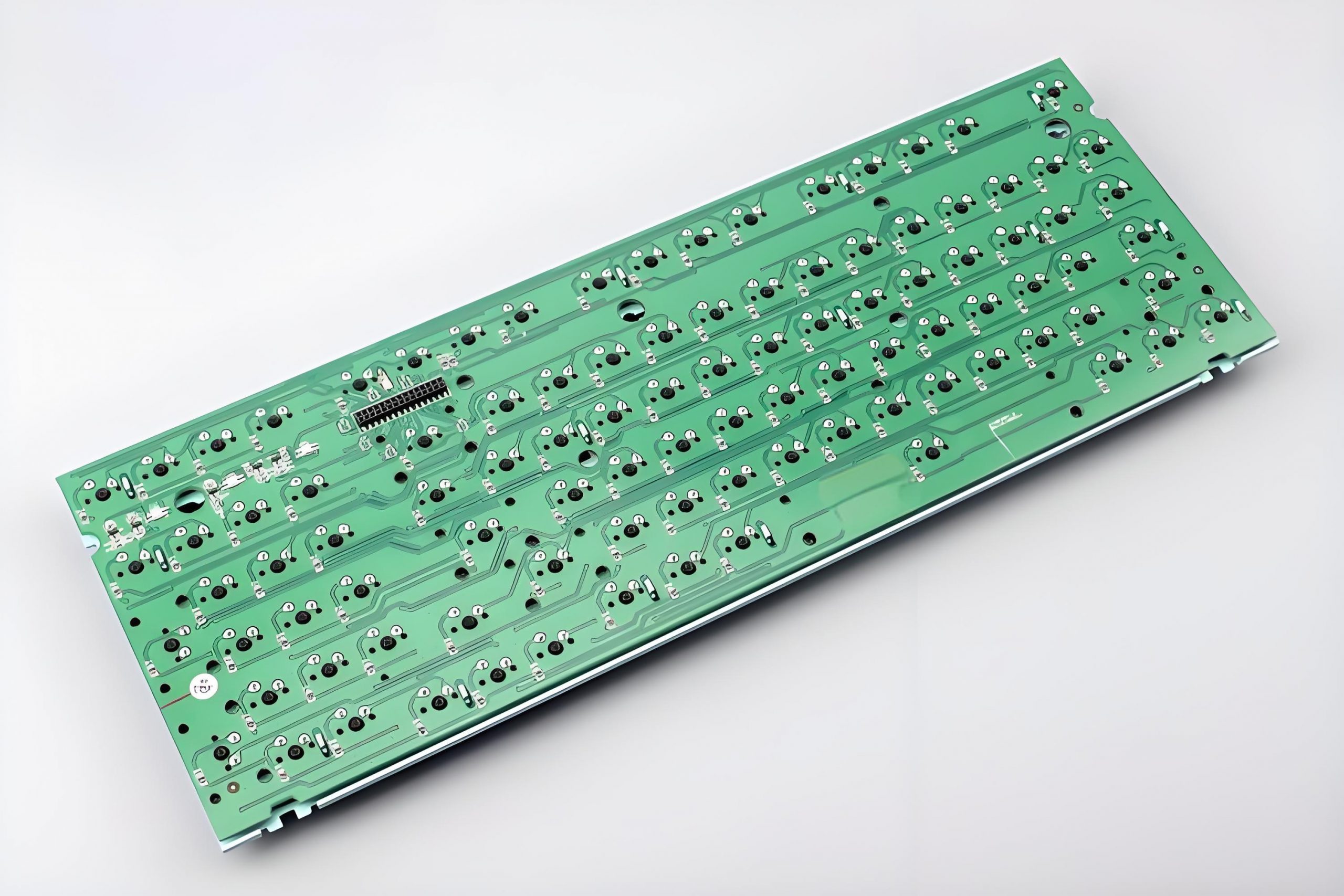
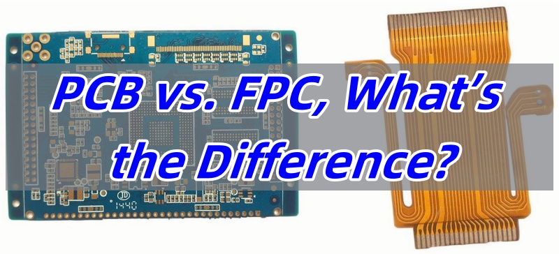
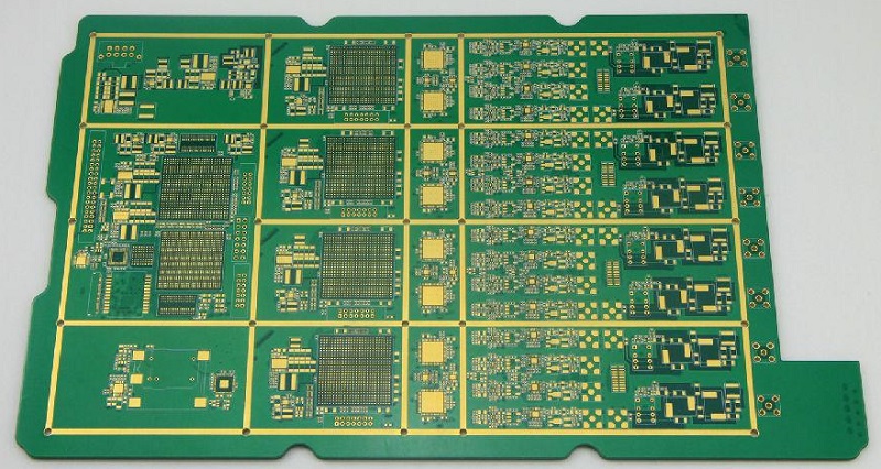
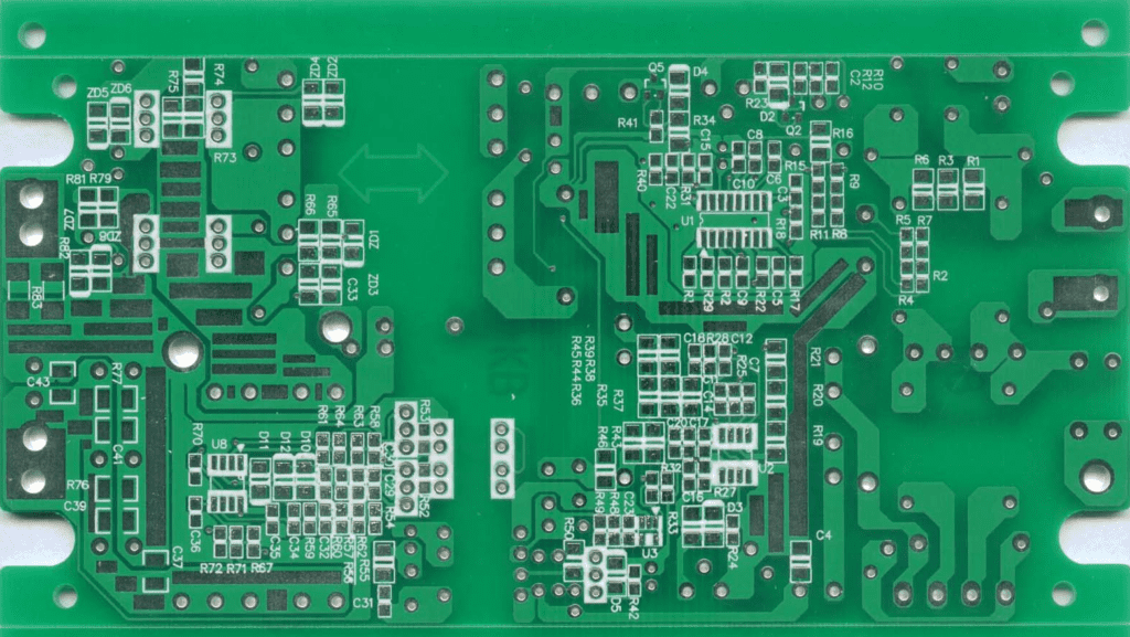
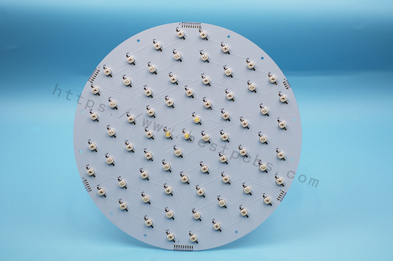
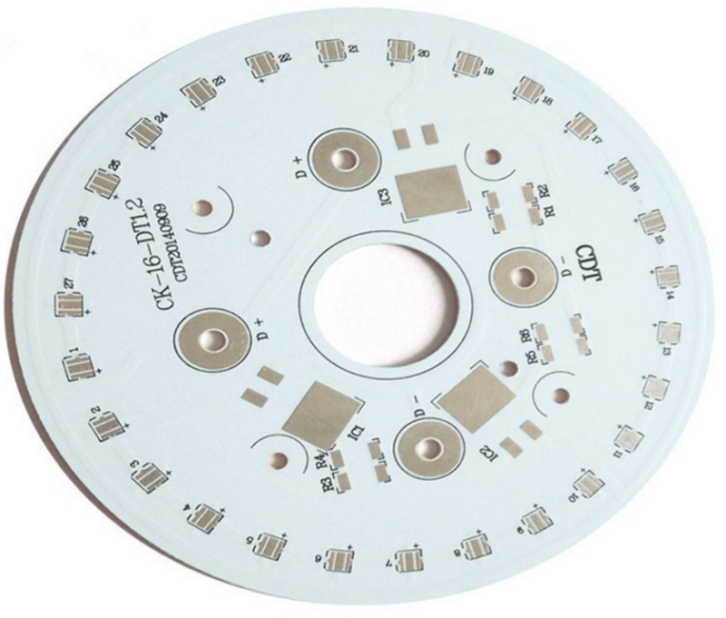
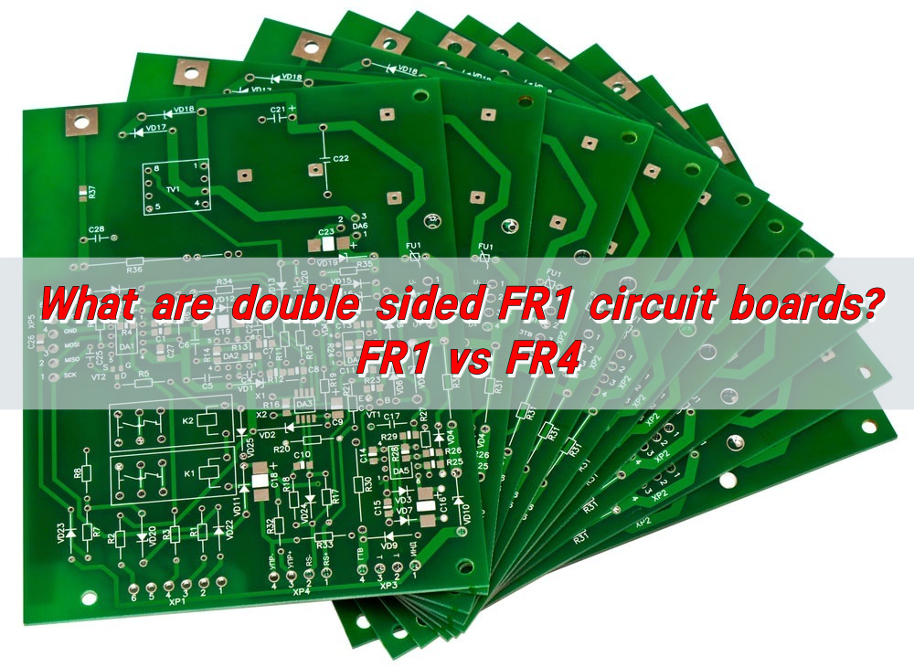
Double Sided FR1 Circuit Boards are a type of printed circuit board (PCB) made of FR1 material with two layers of conductive traces. FR1 is a flame retardant material made of paper base and phenolic resin, with good electrical properties and cost-effectiveness, suitable for a variety of electronic devices.
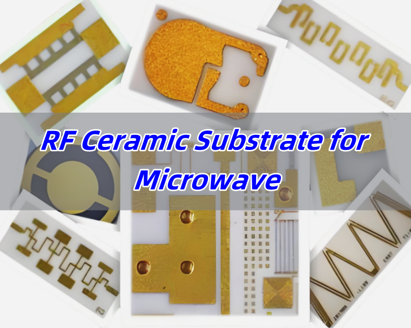
As a PCB manufacturer with more than 18 years of manufacturing experience, BEST Technology has accumulated rich experience and excellent technical strength in the production of double-sided FR1 circuit boards. BEST Technology’s production process uses advanced equipment and a strict quality control system to ensure that each circuit board meets high quality standards.
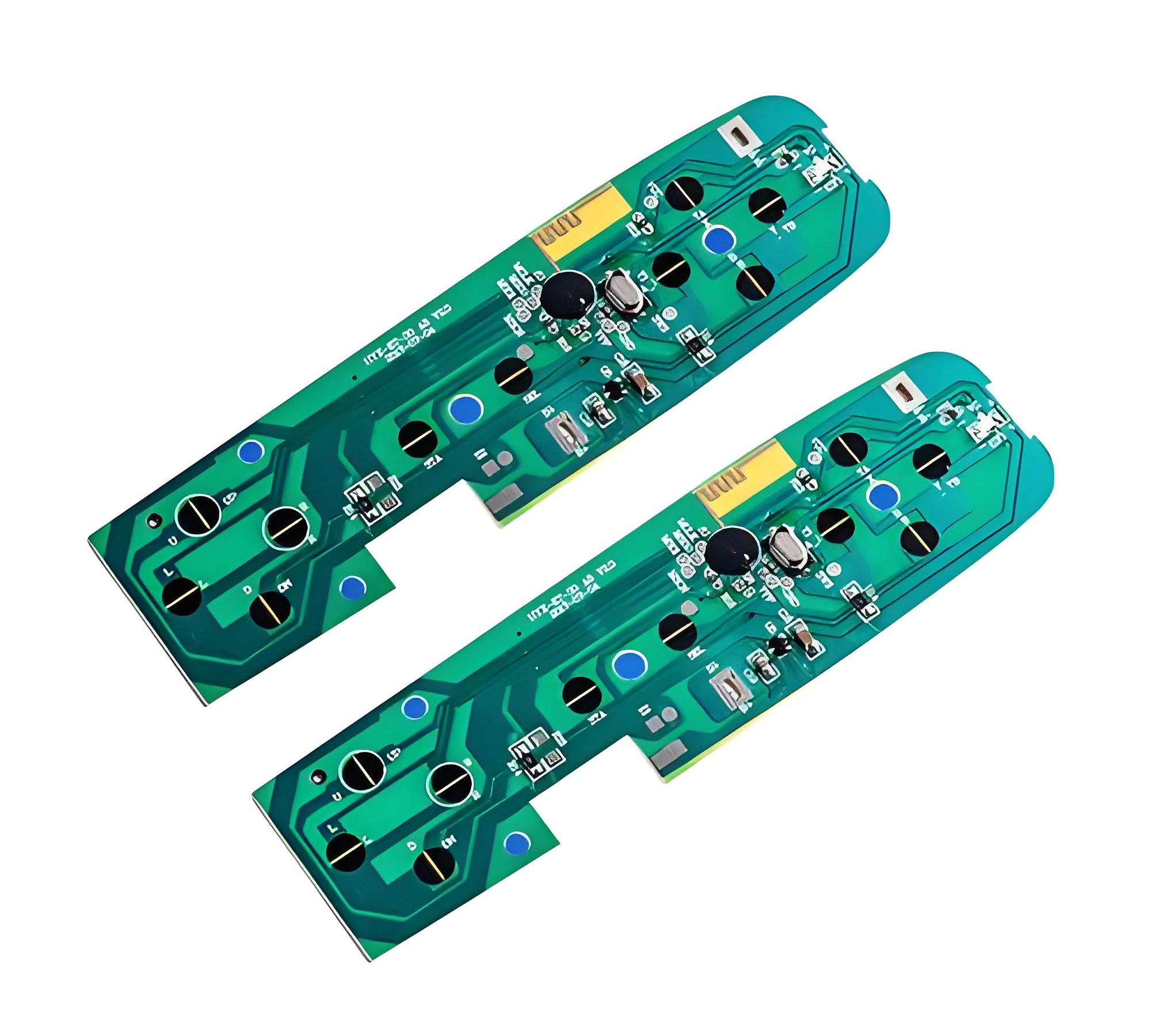
What are double sided FR1 circuit boards?
A double-sided FR1 PCB is made from Flame Retardant 1 (FR1) material, a paper-based phenolic laminate that serves as the board’s substrate. The defining characteristic of double-sided PCBs is their copper layers on both sides, allowing components to be soldered on both surfaces.
This feature enables denser circuit layouts, making double-sided FR1 PCBs ideal for applications where single-layer boards cannot provide enough space for circuit traces.
However, because FR1 is not as heat-resistant as FR4, it is mainly used in low-power electronic devices that do not generate excessive heat.
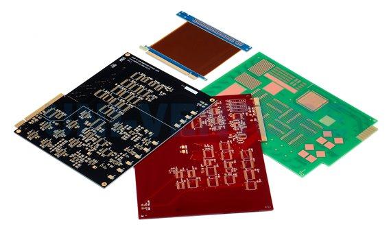
What is the difference between FR1 and FR4 PCB?
FR1 and FR4 are two different types of PCB materials, each suited for specific applications. Here’s how they compare:
Material Composition:
- FR1: Made of phenolic resin and paper-based material.
- FR4: Constructed from woven fiberglass and epoxy resin, making it more rigid and durable.
Thermal Resistance:
- FR1: Has a lower heat tolerance, making it unsuitable for high-temperature applications.
- FR4: Withstands higher temperatures, ideal for demanding environments.
Durability & Strength:
- FR1: More brittle, making it prone to cracking under stress.
- FR4: Has high mechanical strength, suitable for multilayer PCBs.
Cost:
- FR1: Cheaper, making it ideal for cost-effective projects.
FR4: More expensive but offers better longevity.
Common Uses:
- FR1: Found in household electronics, small gadgets, and simple power circuits.
- FR4: Used in industrial, automotive, and high-performance electronic devices.
What is FR1 FR2 and FR3?
Many PCB materials exist, but FR1, FR2, and FR3 are closely related. All are paper-based but with different properties:
- FR1: Phenolic resin impregnated kraft paper substrate, with the highest heat resistance (UL 94 V-0/V-1) among the three, used for single-layer boards and basic double-sided boards (lighting equipment, home appliance control boards), with the lowest cost but poor moisture resistance and low dimensional stability.
- FR2: Phenolic resin paper-based material, with lower heat resistance than FR1 (UL 94 V-2), mainly used for low-cost single-layer PCBs (remote controls, toy circuits), with high flammability and requiring fireproof coating and not suitable for high temperature environments.
- FR3: Epoxy resin impregnated paper-based material, with significantly improved moisture resistance, suitable for basic consumer electronics circuits (mobile phone chargers, small home appliances), as a compromise between FR2 and FR4, but with limited high temperature resistance.
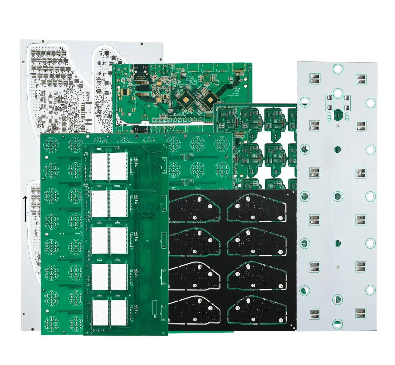
What is the difference between single-sided and double-sided PCBs?
Single-sided PCB: Copper is only coated on one side (commonly used FR1/FR2 paper-based materials), made by simple etching process, with low manufacturing cost but limited design flexibility, and complex connections require jumper wires.
Double-sided PCB: Copper is coated on both sides and uses via interconnection technology (mostly using FR3/FR4 substrates), supports double-sided layout of components and multi-layer wiring. The manufacturing cost is higher but the reliability is significantly improved.
How to make double sided FR1 circuit boards?
Manufacturing double-sided FR1 PCBs involves several steps:
- Material preparation: Double-sided copper-clad FR1 phenolic paper substrate is selected. Its heat resistance (UL 94 V-0/V-1) and cost balance characteristics are suitable for basic double-sided board requirements.
- Circuit design: Use tools to complete the Gerber file, focus on optimizing the via distribution and copper foil thickness (usually 35μm), and ensure that the mechanical strength of the FR1 substrate is stable during the etching process.
- Photoresist and etching: Double-sided negative photosensitive dry film is coated, and after exposure and development, a resist pattern is formed, and the circuit is etched out using a solution.
- Drilling and metallization: CNC drilling machine processes through holes, chemical copper plating combined with electroplating copper achieves double-sided conduction, and the FR1 substrate needs to be pre-impregnated to enhance the bonding strength.
- Solder mask and silk screen printing: Screen printing thermosetting solder mask ink forms a protective layer, and character logos are printed at the same time.
- Assembly and testing: Wave soldering or manual soldering of components, ICT testing after flying probe test of conductivity, FR1 board needs to avoid long-term use in high temperature environment.
What are the advantages of double sided FR1 circuit boards?
Double-sided FR1 PCBs offer several benefits:
- Cost-Effective: One of the most affordable PCB options, making it ideal for budget-sensitive projects.
- Lightweight: FR1 is lighter than FR4, making it easier to handle.
- Good Electrical Insulation: The phenolic resin provides stable electrical performance.
- Efficient for Simple Electronics: Works well in basic circuit designs, power supplies, and consumer electronics.
What are the disadvantages of double sided FR1 circuit boards?
While FR1 PCBs are useful, they have some drawbacks:
- Lower Heat Resistance: Can degrade in high-temperature environments.
- Brittle: More fragile than FR4, leading to possible breakage under mechanical stress.
- Limited Multilayer Capability: Unlike FR4, FR1 does not support complex multilayer stacking.
- Moisture Absorption: Can absorb moisture over time, affecting durability.
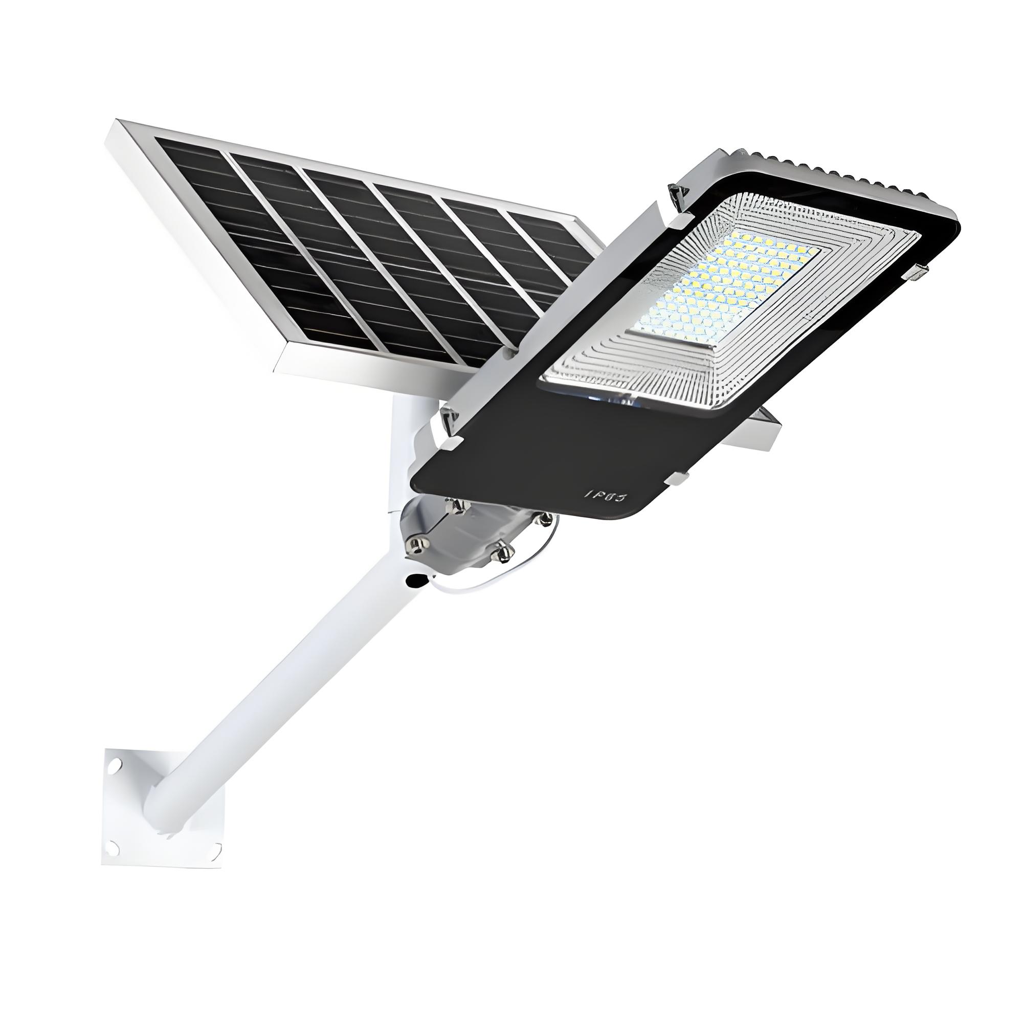
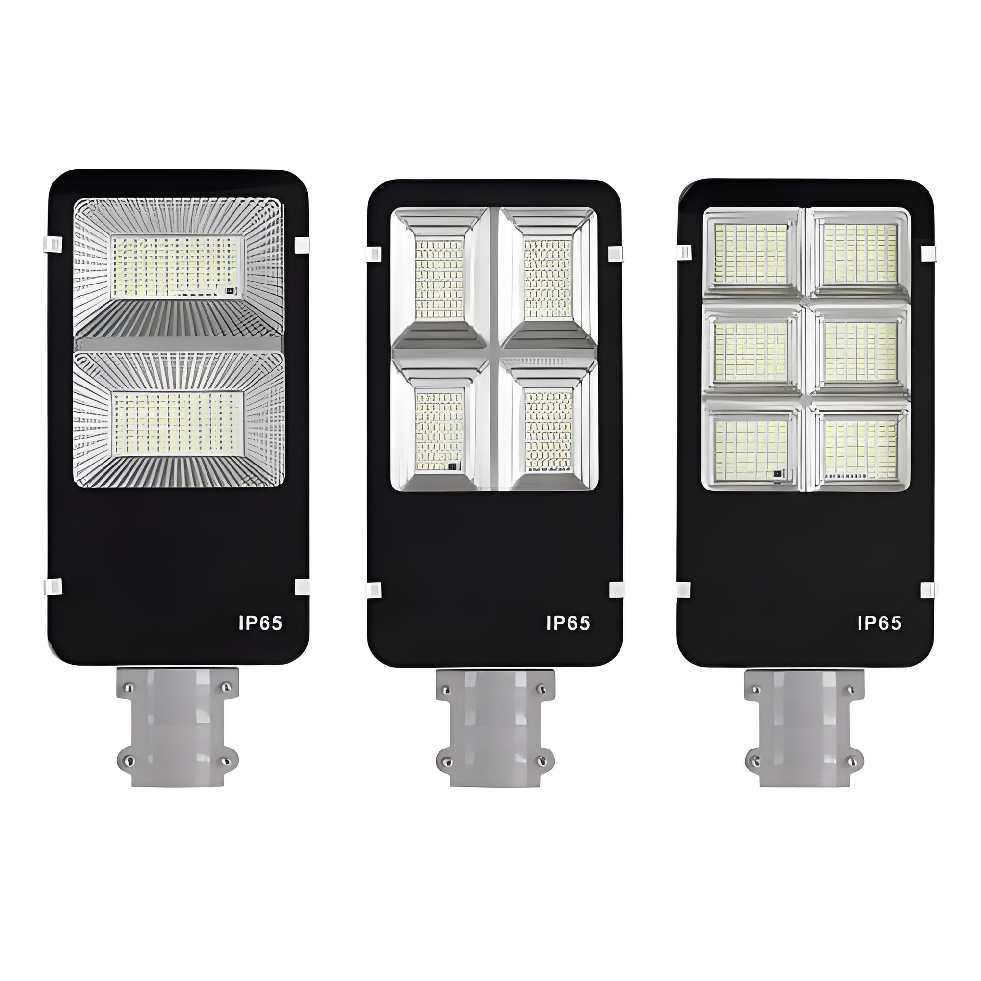
What are the applications of double sided FR1 circuit boards?
Due to its affordability and reliability, double-sided FR1 PCBs are widely used in:
- Consumer Electronics: Found in TV remote controls, LED drivers, and power strips.
- Power Supplies: Used in low-power voltage regulators and adapters.
- Automotive Electronics: Found in basic control modules for car accessories.
- Industrial Control Systems: Used in low-complexity automation circuits.
Conclusion:
Double sided FR1 circuit boards offer an affordable and efficient solution for various electronic applications. Their dual-layer design allows for more compact circuit layouts. While FR1 PCBs may have some limitations, they remain a cost-effective choice for many projects.
At BEST Technology, Whether you need double-sided FR1 PCBs or other custom PCB solutions, we are here to help. Contact us today at sales@bestpcbs.com to discuss your project needs!