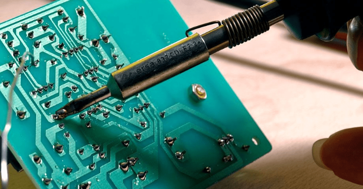
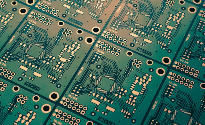
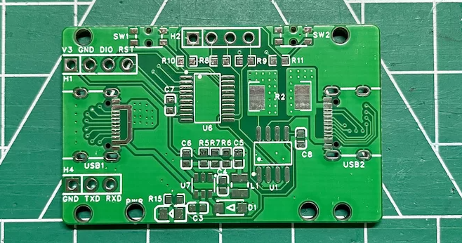
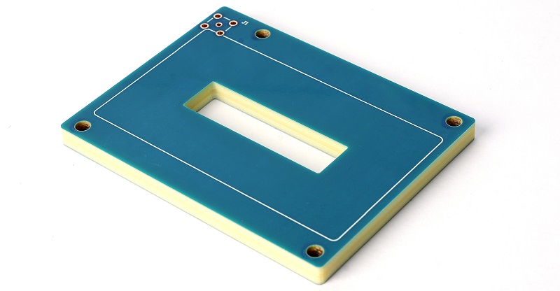
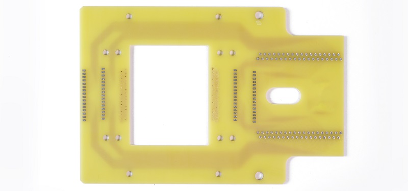
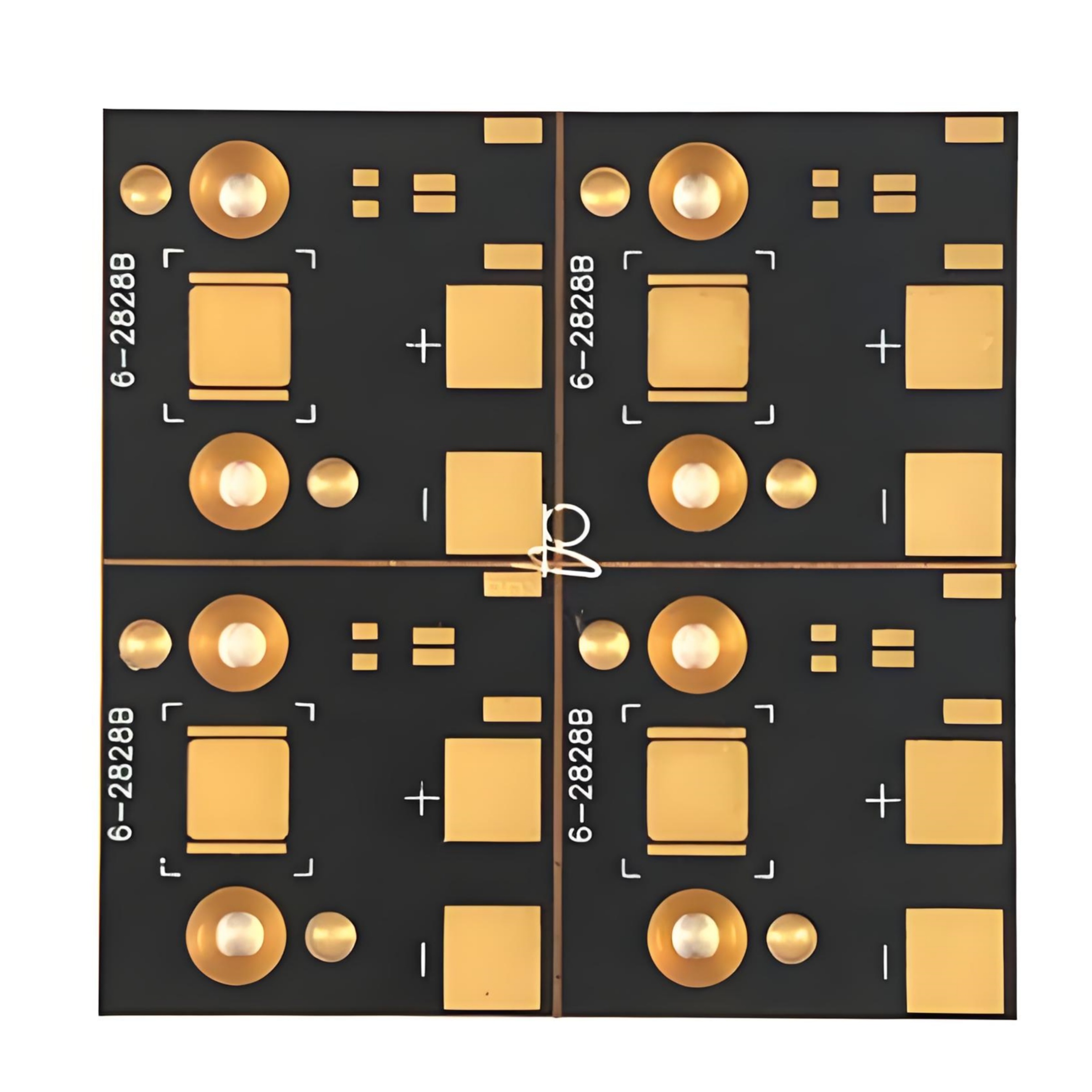
Custom circuit board manufacturers are the backbone of modern electronics. Whether you’re building medical devices, automotive control systems, or IoT gadgets, having the right manufacturer matters. In today’s world, reliability, fast communication, and engineering support are essential.
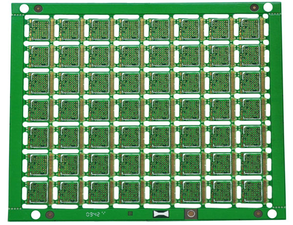
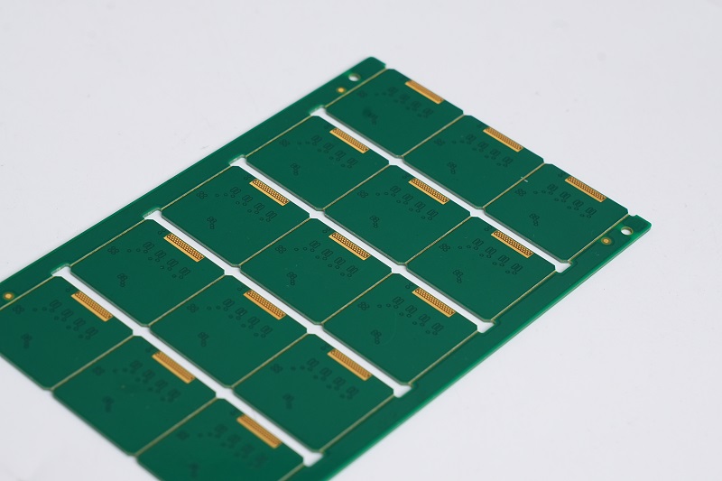
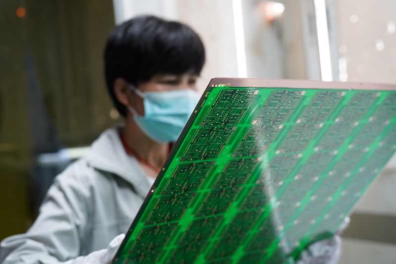
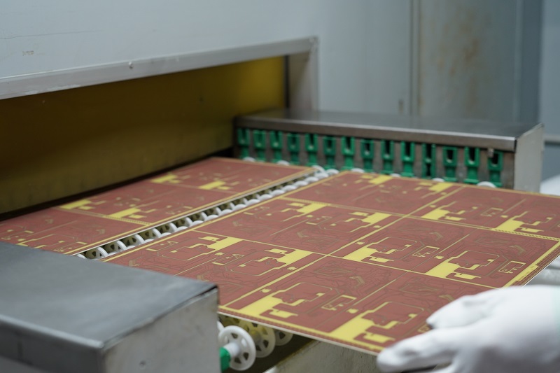
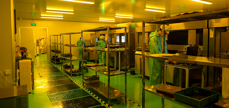
EBest Circuit (Best Technology) is one of the custom circuit board manufacturers in China, providing dedicated customer support and fast service. We stand out because of our wide product range, responsive engineering support, fast quoting, and 24/7 technical assistance. EBest Circuit (Best Technology) offers custom circuit board manufacturing and custom PCBA services in the same house. We have our own SMT factory in Baoan district, Shenzhen. Our PCBA capabilities and wide material sourcing help customers reduce procurement time. If you have any custom circuit board or PCBA project that needs our support, pls email us at sales@bestpcbs.com.
What Are the Best Custom Circuit Board Manufacturers?
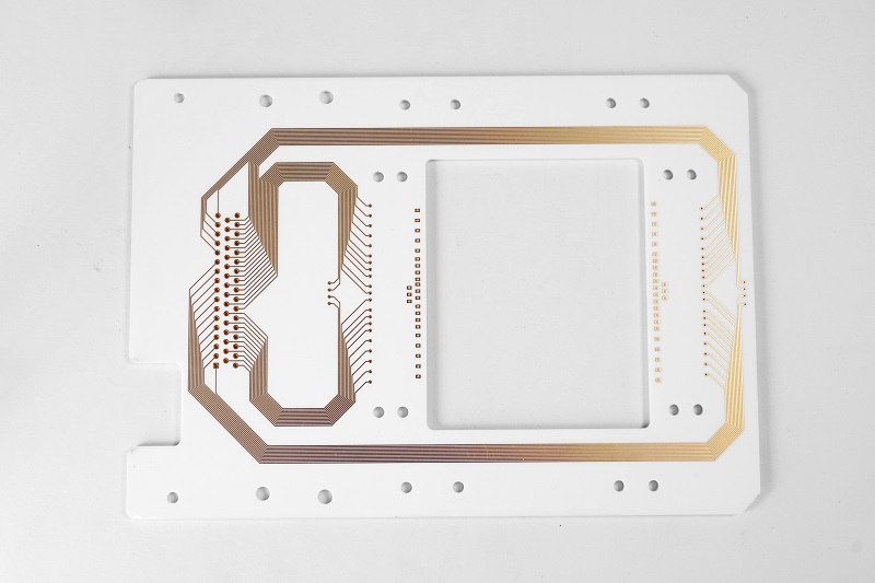
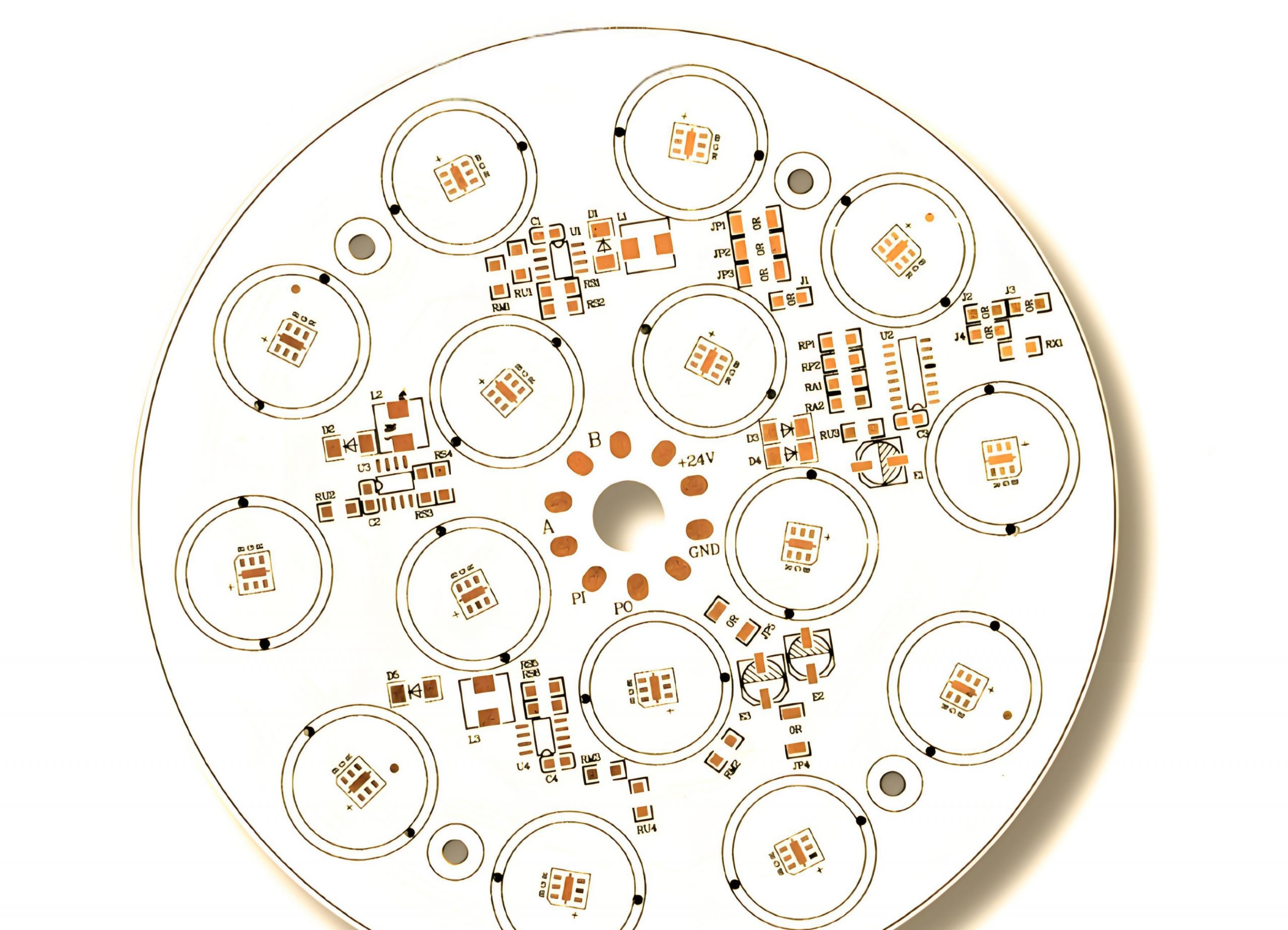
The best manufacturers are not just PCB makers. They are partners in your design journey. They support your ideas, correct design mistakes early, and ensure manufacturability from the start. These companies provide complete solutions, not just production. They handle every stage, from design reviews to assembly, to prevent common design flaws like acid traps or misaligned vias. Their ability to handle HDI and flex-rigid boards is another plus.
Who to Make Custom Circuit Board?
If you’re looking for a dependable PCB partner, EBest Circuit (Best Technology) is the one to work with. EBest Circuit (Best Technology) does not just make boards that provide the solutions to suit your project. With deep experience in HDI, flexible PCBs, and microwave materials, Our team helps reduce design errors and shorten lead times. Our engineering team works closely with customers to adjust files to fit real-world manufacturing. That reduces rework, boosts yield, and keeps your timelines on track.
Who Is the Biggest Custom Circuit Board Supplier in the USA?
There are several strong custom circuit board manufacturers USA based. These companies serve a wide range of industries and have solid reputations for quality and scale.
1. Advanced Circuits: One of the largest in the U.S., known for quick turns and in-house DFM checks. They serve aerospace and medical clients too.
2. Sanmina: A large EMS company with full PCB manufacturing and assembly capabilities. Well-known in telecom.
In short, these firms stand out for their service levels, product range, and strong communication.
How to Choose Custom Circuit Board Manufacturers?
When choosing a manufacturer, don’t only look at price. You need to evaluate:
1. Engineering Support: Can they assist with layout reviews and catch issues before production?
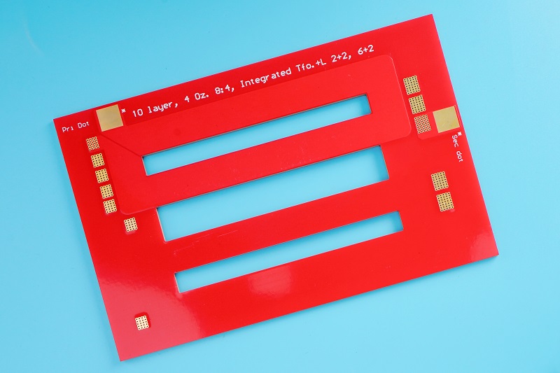
2. Material Sourcing: Do they offer options like Rogers, polyimide, or hybrid stack-ups?
3. Response Time: Are they available when you need changes or updates?
4. Manufacturing Flexibility: Can they handle prototypes, small runs, and mass production?
5. Certifications: Do they hold ISO 13485, IATF 16949, or AS9100D?
Companies like EBest Circuit (Best Technology) check all these boxes. They understand that every design choice affects the final outcome. Their help reduces costly revisions and lost time.
How Do I Find the Custom Circuit Board Manufacturers?
Start with online platforms. A quick search for on-time delivery custom PCB manufacturer or custom MCPCB brings many options. But be cautious. Reviews and case studies matter. Check for customer success stories, certifications, and if they offer real-time quotes. Also, reach out to their sales or support. Good manufacturers answer fast and clearly.
EBest Circuit (Best Technology) stands out because they respond quickly, no matter your time zone. Our 24/7 tech support ensures your questions never wait. Whether you are prototyping or scaling up, our support keeps things smooth.
Why Should I Choose EBest Circuit (Best Technology) as One of My Trusted Custom Circuit Board Manufacturers?
EBest Circuit (Best Technology) has the competitive advantages as following:
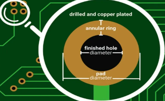
1. Technical Barriers & Design Support: Many clients struggle with design flaws, especially with HDI or FPC. EBest Circuit (Best Technology) offers pre-production design checks, including acid trap analysis, pad alignment, and DFM support. This reduces rework and scrap.
2. Accurate Quotes & Cost Control: Custom PCBs often require special materials and processes. BEST uses a refined quoting system that avoids surprises. We help you understand what drives cost and where to adjust for savings.
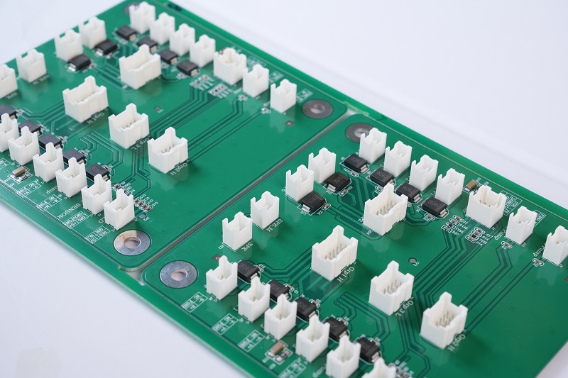
3. Supply Chain & Delivery: From samples to large runs, BEST tracks your order closely. Our MES system ensures material traceability and status updates at each step. For high-frequency boards, we plan material sourcing early to avoid delivery issues.
4. Certifications & Trust: We hold ISO 9001, ISO 13485, IATF 16949, and AS9100D. This means your boards are ready for medical, automotive, and aerospace use. Your projects pass audits and meet compliance faster.
5. 24/7 Technical Support: EBest Circuit (Best Technology) runs a real-time support system. This keeps your production moving. If something changes or a file needs fixing, someone is available to help — day or night. That’s how they reduce downtime and increase your uptime.
EBest Circuit (Best Technology) isn’t just a custom circuit board maker. We’re your partner from start to finish. Our people understand that success isn’t just about the board — it’s about speed, accuracy, and support. That’s what builds long-term partnerships and steady growth.
In conclusion, custom circuit board manufacturers shape the products we use every day. But not all are created equal. The best go beyond basic services. They guide your design, ensure fast response, and give you tailored solutions. They help prevent costly errors and make sure each board is built right the first time.
EBest Circuit (Best Technology) is among the best custom circuit board manufacturers you can work with. We place a high priority on your specific requirements from quoting to delivery. Our 24/7 technical team means no delays. Our engineering team prevents design failures before they happen. And with 19 years of industry experience, your project is always in good hands. If you want reliable quality, faster feedback, and smarter support, reach out to EBest Circuit (Best Technology) at sales@bestpcbs.com. We’ll help you move from design to delivery without stress. With BEST, we ensure you a custom circuit board success.