Looking for PCB manufacturer in Syria? This blog is mainly about the pain points and our solutions of Syria PCB manufacturing, recommend global PCB manufacturer.
Syria’s PCB manufacturing industry is struggling to recover amid post-conflict industrial damage and external sanctions. PCB manufacturer in Syria underpins the local electronic manufacturing sector, but faces tangible hurdles: most operational facilities rely on outdated equipment (a common issue across Syrian industries), daily power supply is limited to just a few hours, and raw material imports are hindered by shipping restrictions and high costs. These challenges directly constrain the development of PCB manufacturer in Syria, limiting their technical capacity. For those seeking local PCB solutions, grasping the real limitations of Syria PCB manufacturer is key to project success. Syria PCB Manufacturing is slowly adapting to market needs, but falls far short of international standards for high-precision and large-scale production.
Are you Facing these Challenges of Syria PCB Manufacturing?
- Is it difficult to obtain high-precision PCB prototyping services due to outdated equipment of local PCB Manufacturer in Syria?
- Do you often face delays in project progress due to unstable raw material supply of Syria PCB Manufacturing?
- Is there a lack of professional technical support when encountering design compatibility issues in PCB Syria production?
- Do you worry about product quality risks caused by the incomplete quality control system of local Syria PCB Factory?
- Is it challenging to meet the urgent order demand due to the slow production efficiency of Syria PCB Company?
Full-Process Guarantee from Demand to Delivery
- Precise Demand Confirmation: Provide one-to-one consulting services to deeply understand project requirements, avoid misunderstandings, and lay a foundation for subsequent production.
- Professional Design Optimization: Integrate free DFM analysis into the early stage, solve design compatibility problems in advance, and improve production pass rate.
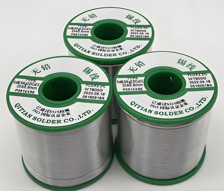
- Stable Raw Material Supply: Establish global high-quality raw material supply chains to avoid production interruptions caused by raw material shortages, ensuring stable production of PCB Manufacturer in Syria-related orders.
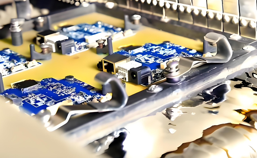
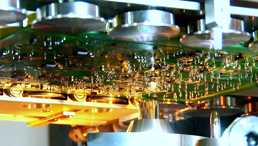
- High-Precision Production Control: Adopt advanced production equipment and strict process standards to realize high-precision manufacturing of PCB Syria products, meeting diverse precision requirements.
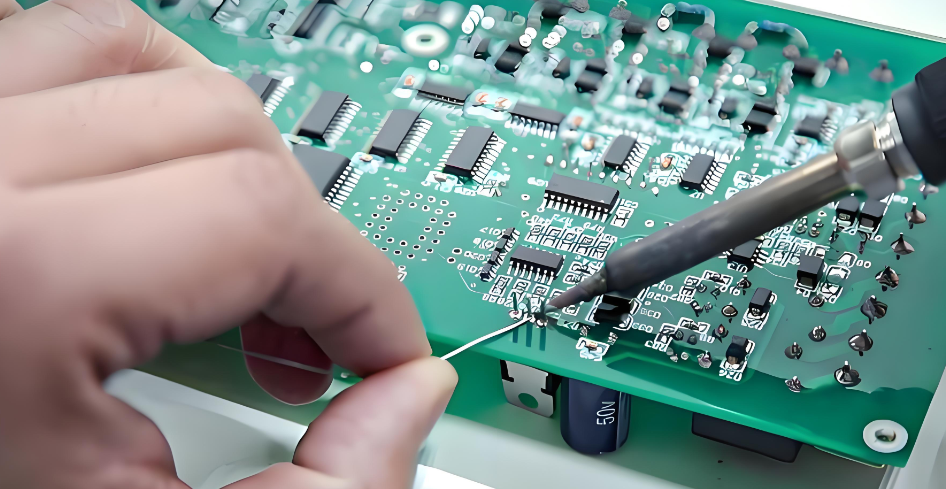
- Comprehensive Quality Inspection: Implement full inspection for mass production, with multiple quality inspection links including visual inspection, electrical performance testing and reliability testing to ensure product quality.
- Efficient Delivery Guarantee: Open up green channels for urgent orders, realize 24-hour rapid prototyping, and ensure 99.2% on-time delivery rate for mass production.
- Thoughtful After-Sales Service: Provide technical support and problem-solving solutions after delivery, ensuring smooth use of products.
Why Syrian Clients Choose Best Technology(EBest Circuit) for PCB Manufacturer?
- Competitive Pricing: Targeted strategies for Syria market. Our cost-sensitive solutions cut PCB manufacturing costs by 18% on average, with bulk order discounts up to 25%, achieved without quality compromise.
- 24-Hour Rapid Prototyping: 99.8% on-time delivery for 1/2/4-layer urgent prototypes within 24h. Cuts product verification cycle by 50% vs Syria’s industry average, seizing market opportunities fast.
- Fast & Reliable Delivery: 99.2% on-time rate for mass production in Syria. 7-12 working days average delivery, 30% faster than local average, with real-time order tracking.
- Superior Quality Assurance: 28 strict quality checks, 100% full inspection for mass production. 99.9% pass rate, <0.1% defect rate, avoiding rework costs from quality issues.
- 19 Years of Experience: Served 2,000+ Syria-based customers, completed 5,000+ custom projects. Deep local market insights cut costs by 15-20% on average and boost efficiency.
- Free DFM Analysis: Identifies 4+ design risks per project. Reduces modifications by 60%, shortens cycle by 30%, and boosts qualification rate by 17%.
- Global Certifications: ISO9001/13485, REACH, RoHS, IATF16949. Meets standards of 120+ countries, improving export pass rate by 40% for Syrian customers.
- One-Stop Service: Covers design optimization, prototyping, production & assembly. Reduces supplier docking time by 40%, meeting diverse needs from small-batch to mass production.

Our PCB Prototyping Service
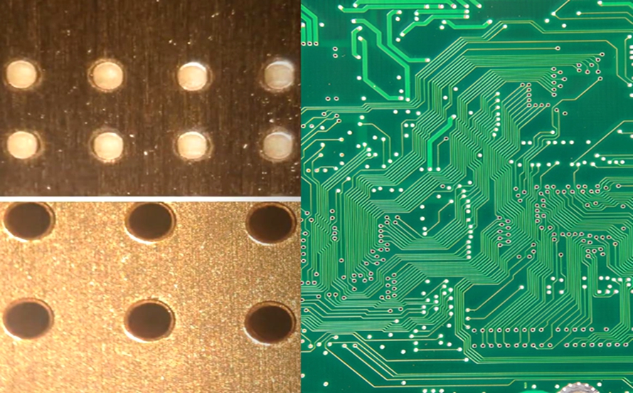
Our PCB prototyping service is tailored to meet the needs of rapid product verification and iteration in the Syria electronics industry. We support a variety of prototype types, including single-layer, double-layer and multi-layer PCBs, with a minimum line width/line spacing of 3mil/3mil and a minimum hole diameter of 0.1mm.
As a professional Syria PCB plant partner, we use high-quality substrates and advanced processing technology to ensure that prototypes have the same performance as mass-produced products. The prototyping cycle is flexible, with 24-hour rapid delivery for urgent orders and 3-5 working days for regular orders. In addition, we provide free visual inspection and electrical testing for prototypes to ensure that every sample meets the design requirements, helping you quickly verify the feasibility of your products and accelerate the R&D process.
Our Prototyping Lead Time
| Layers | Normal Service | Fastest Service |
| 1 | 7 Days | 24 H |
| 2 | 8 Days | 24 H |
| 4 | 10 Days | 48 H |
| 6 | 10 Days | 72 H |
| 8 | 12 Days | 72 H |
| ≥10 | TBD | TBD |
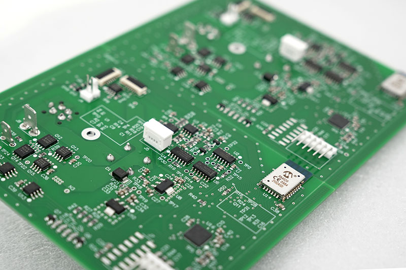
Our PCB Manufacturing Capability
| Item | Capabilities |
| Layer Count | 1 – 32 Layers |
| Max Board Dimension | 2424″ (610610mm) |
| Min Board Thickness | 0.15mm |
| Max Board Thickness | 6.0mm – 8.0mm |
| Copper Thickness | Outer Layer: 1oz~30oz, Inner Layer: 0.5oz~30oz |
| Min Line Width/Line Space | Normal: 4/4mil (0.10mm); HDI: 3/3mil (0.076mm) |
| Min Hole Diameter | Normal: 8mil (0.20mm); HDI: 4mil (0.10mm) |
| Min Punch Hole Dia | 0.1″ (2.5mm) |
| Min Hole Spacing | 12mil (0.3mm) |
| Min PAD Ring(Single) | 3mil (0.075mm) |
| PTH Wall Thickness | Normal: 0.59mil (15um); HDI: 0.48mil (12um) |
| Min Solder PAD Dia | Normal: 14mil (0.35mm); HDI: 10mil (0.25mm) |
| Min Soldermask Bridge | Normal: 8mil (0.2mm); HDI: 6mil (0.15mm) |
| Min BAG PAD Margin | 5mil (0.125mm) |
| PTH/NPTH Dia Tolerance | PTH: ±3mil (0.075mm); NPTH: ±2mil (0.05mm) |
| Hole Position Deviation | ±2mil (0.05mm) |
| Outline Tolerance | CNC: ±6mil (0.15mm); Die Punch: ±4mil (0.1mm); Precision Die: ±2mil (0.05mm) |
| Impedance Controlled | Value>50ohm: ±10%; Value≤50ohm: ±5ohm |
| Max Aspect Ratio | 0.334027778 |
| Surface Treatment | ENIG, Flash Gold, Hard Gold Finger, Gold Plating(50mil), Gold finger, Selected Gold plating, ENEPIG, ENIPIG; HAL, HASL(LF), OSP, Silver Immersion, Tin Immersion |
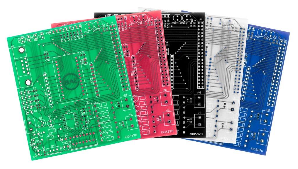
| Soldermask Color | Green/White/Black/Yellow/Blue/Red |
Case Studies of Syria PCB Manufacturing Project
Project Background: A local electronics enterprise in Syria needed PCB products for industrial control equipment, which required high stability and resistance to harsh environmental conditions (high temperature and dust) in Syria.
Project Requirements: The PCB needed to be a 6-layer board with high precision, comply with RoHS and ISO13485 certifications, and the delivery time of prototypes was required to be within 48 hours, with a mass production delivery time of 15 working days.
Project Difficulties: The harsh climate in Syria made high requirements on the heat resistance and corrosion resistance of the PCB; the tight delivery time put forward high requirements on the production efficiency; the complex 6-layer board design needed professional optimization to ensure signal integrity.
Our Solutions:
- Selected high-temperature resistant and corrosion-resistant substrate materials to adapt to the local environmental conditions;
- Launched the urgent prototyping process, arranged special production lines to complete the prototype production within 48 hours;
- Conducted free DFM analysis on the design scheme, optimized the line layout and hole position design to ensure signal integrity;
- Adopted strict quality control processes, including high-temperature resistance testing and corrosion resistance testing, to ensure product stability.
Output Results: The prototypes passed all performance tests at one time, and the mass production products were delivered 2 days in advance. The PCB products have been operating stably in the harsh environment of Syria for more than 12 months, with a failure rate of 0.1%.
How to Get A Quote For Syria PCB Project?
1. Define Project Requirements
- Specify PCB specifications: layer count, dimensions, material type (e.g., FR-4, aluminum), surface finish (e.g., HASL, ENIG), minimum trace width/spacing, and special features (e.g., impedance control, via-in-pad).
- Determine quantities (prototypes/mass production), delivery timeline, and quality standards (e.g., IPC Class 2/3).
2. Prepare Technical Documents
- Upload Gerber files (manufacturing files) and BOM (Bill of Materials) to suppliers.
- Include additional details: assembly instructions, component placement files (e.g., Pick-and-Place), 3D CAD models (if applicable), and testing requirements (e.g., flying probe, AOI).
- Clarify any custom needs (e.g., RoHS compliance, thermal management solutions).
3. Identify Suppliers
- Search for PCB manufacturers with experience in Middle Eastern markets or international suppliers supporting Syria. Use platforms like Best Technology to source quotes from multiple vendors.
- Verify supplier capabilities: check their website for case studies, certifications (e.g., ISO 9001, UL), and client testimonials.
5. Submit RFQ (Request for Quotation)
- Use the supplier’s online quote form or email their sales team (e.g., sales@mermarinc.com) with project details.
- Include shipping address, preferred delivery method (e.g., DHL, air freight), and payment terms (e.g., wire transfer, credit card).
- Attach files securely (max 30MB via form or file-sharing platforms like WeTransfer).
6. Review and Negotiate Quotations
- Compare quotes for cost breakdown (fabrication, assembly, components, testing, shipping) and lead times.
- Engage with project managers to clarify ambiguities (e.g., material costs, tooling fees) and negotiate pricing for large volumes.
- Request sample production for critical projects to validate quality before mass production.
7. Finalize Agreement
- Sign a contract detailing specifications, delivery schedule, warranty terms, and penalties for delays.
- Confirm payment milestones (e.g., 50% deposit, 50% upon shipment).
- Arrange logistics for end-to-end tracking (e.g., DHL Express) to ensure timely delivery to Syria.
Welcome to contact us to get a free DFM if you have any request for Syria PCB: sales@bestpcbs.com.