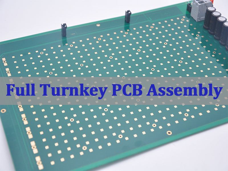
Full turnkey PCB assembly enables companies to streamline PCB fabrication, component sourcing, assembly, and testing under a single accountable manufacturing partner. This article explains how full turnkey PCB assembly works, what services a qualified manufacturer should provide, how full and partial turnkey models differ, and how to choose a reliable turnkey PCB assembly manufacturer in China for long-term project success.
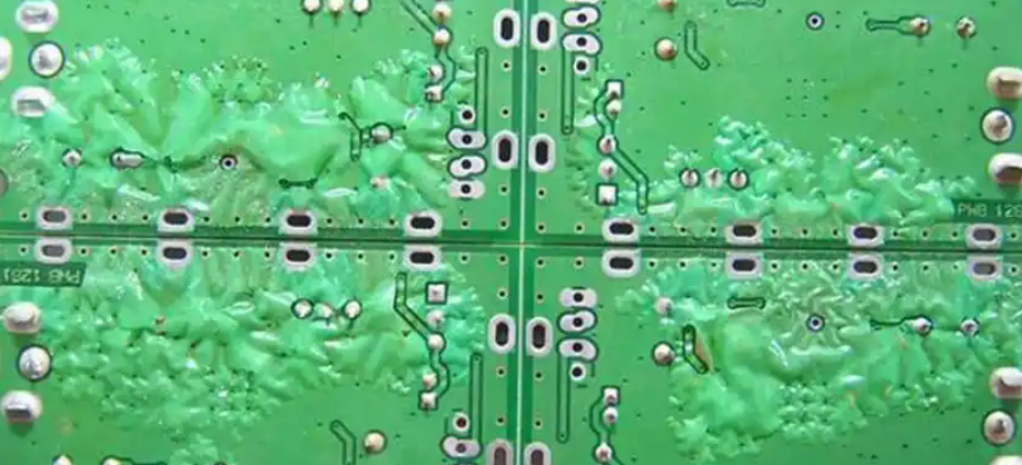
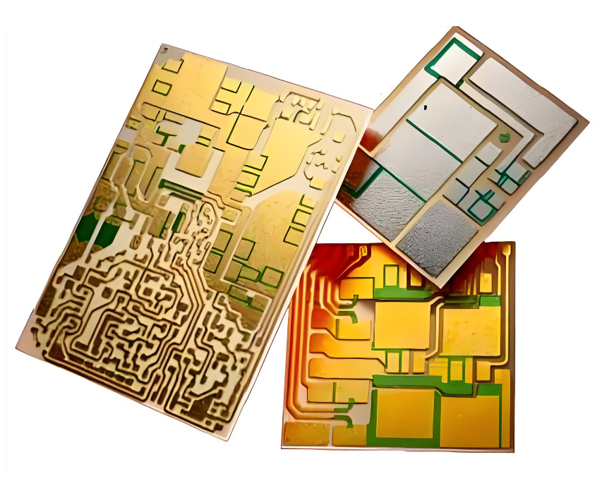
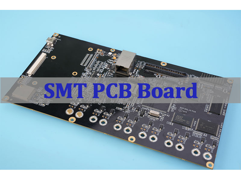
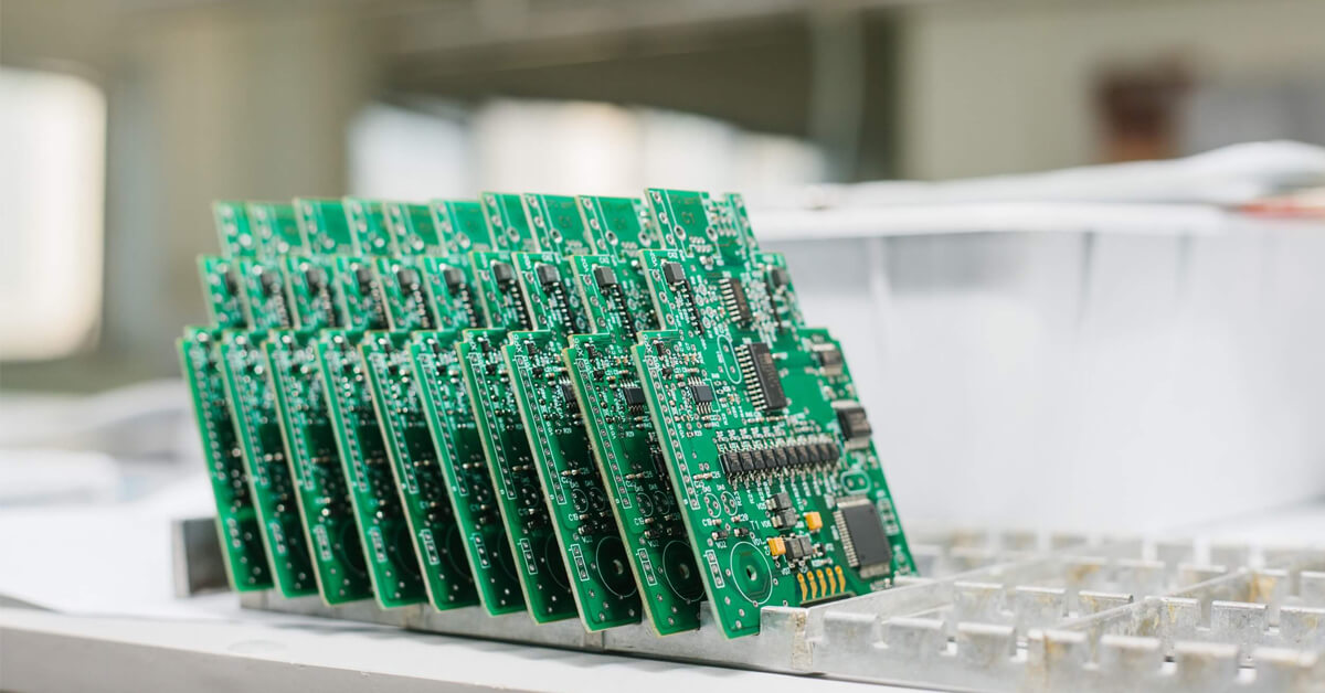
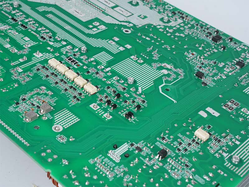
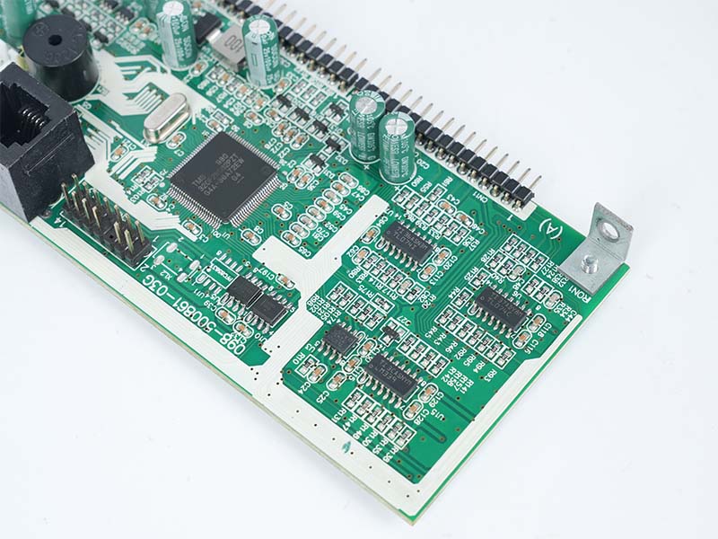
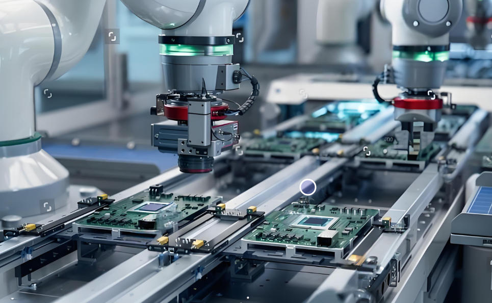
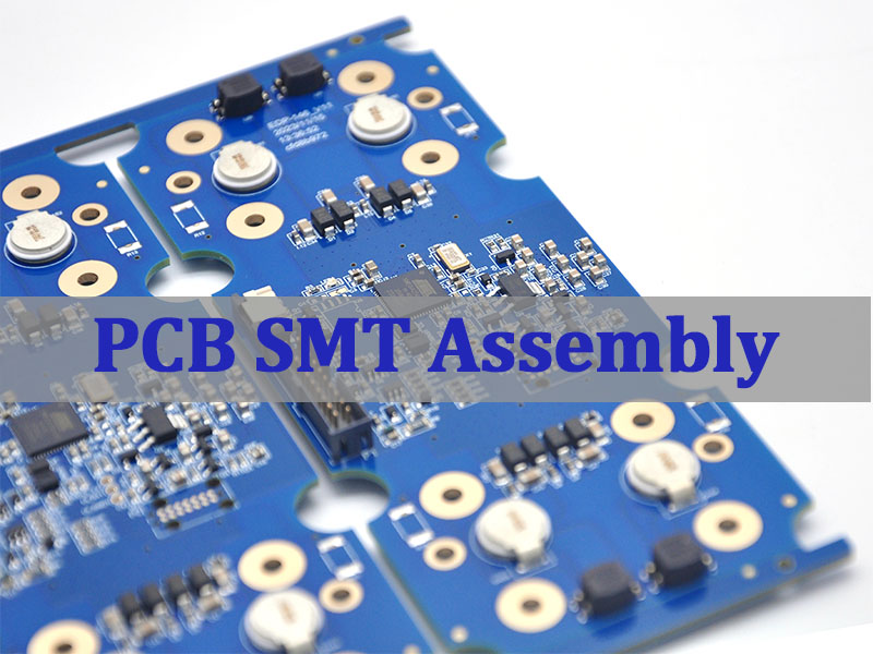
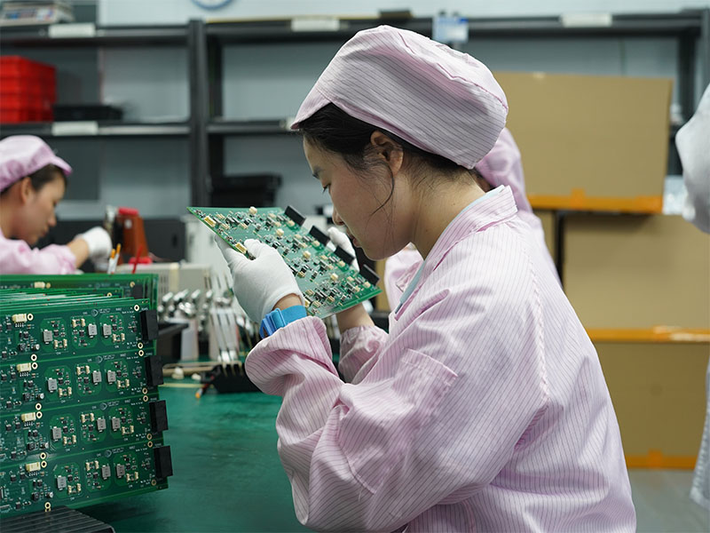
As an established SMT PCB manufacturer, EBest Circuit (Best Technology) provides one-stop PCBA services covering PCB fabrication, component sourcing, SMT/THT assembly, testing, and final integration. Our engineers and sales teams understand the nuts-and-bolts of product design, manufacturing processes, and internal workflows, enabling us to collaborate efficiently with customers and execute projects with clarity and speed. A wide range of PCB assembly services is on offer, including FR-4 PCB, HDI PCB, extra-thin PCB, bus bar PCB, and heavy copper PCB assemblies to support diverse application requirements.
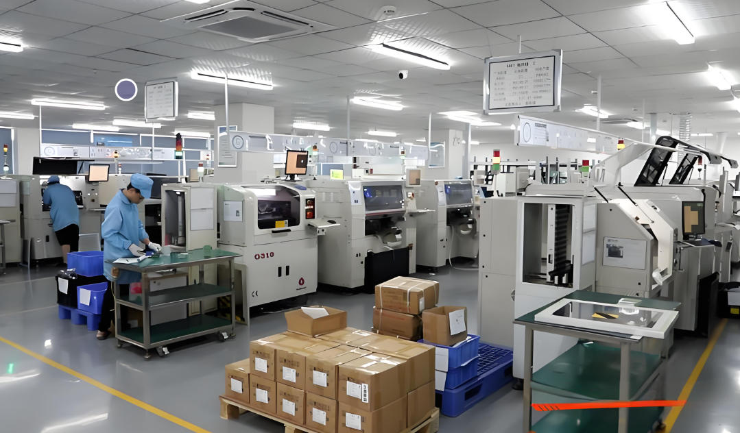
All manufacturing equipment in our facilities is integrated with MES systems, ensuring full traceability for medical PCBs, IoT PCBs, and industrial PCB products throughout the production lifecycle. If you would like to visit our manufacturing facilities on-site to review equipment and production environments, please feel free to contact us at sales@bestpcbs.com.
What Is Full Turnkey PCB Assembly and How Does It Work?
Full turnkey PCB assembly is a manufacturing model in which a single supplier takes end-to-end responsibility for the entire PCBA process—from PCB fabrication and component sourcing to SMT/THT assembly, testing, and final delivery. Instead of coordinating multiple vendors, customers work with one manufacturer accountable for quality, cost, and schedule.
From an engineering standpoint, this model reduces interface risk between PCB manufacturing and assembly. From a procurement perspective, it simplifies supplier management and shortens decision cycles. In practice, full turnkey PCB assembly is widely used for prototype, low-volume, and production projects where supply-chain stability and accountability matter more than unit price alone.
Top 10 Full Turnkey PCB Assembly Manufacturers in China
China has a mature and highly diversified electronics manufacturing ecosystem. In the field of full turnkey PCB assembly, leading manufacturers typically specialize in different board types and service models—ranging from standard FR-4 PCBA to ceramic PCBA, metal-core PCBA, and high-mix industrial assemblies. Below are representative full turnkey PCB assembly manufacturers in China that are commonly evaluated by international engineering and sourcing teams.
1. EBest Circuit (Best Technology)
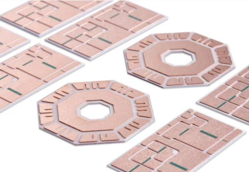
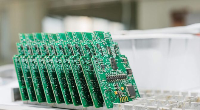
EBest Circuit is a professional full turnkey PCB assembly manufacturer offering in-house PCB fabrication, component sourcing, SMT/THT assembly, testing, and box-build services. The company supports FR-4, HDI, metal-core, ceramic, and rigid-flex PCBs, with strong emphasis on engineering-led DFM review and project coordination. It is widely chosen for prototype, low-volume, and high-mix turnkey projects requiring stable quality and clear accountability.
2. Shennan Circuits (SCC)
Shennan Circuits is a large-scale Chinese manufacturer with strong capabilities in high-layer-count PCBs and complex PCBA. It is commonly associated with telecom, automotive, and industrial electronics, and provides turnkey services mainly for medium-to-high volume production.
3. Kinwong Electronic
Kinwong focuses on advanced PCB manufacturing combined with PCBA services, particularly for automotive electronics and high-reliability industrial products. Its turnkey services emphasize process consistency and long-term supply stability.
4. TTM Technologies China Operations
TTM’s China facilities support full turnkey PCB assembly for high-reliability markets such as aerospace, defense, and industrial controls. The company is known for strict quality systems and complex multilayer PCB integration.
5. WUS Printed Circuit (WUS PCB)
WUS provides PCB fabrication and turnkey PCBA services with strengths in HDI and fine-pitch assemblies. It is often selected for consumer electronics and communication equipment requiring precision manufacturing.
6. Jabil China
Jabil operates as a global EMS provider with full turnkey capabilities in China. Its services focus on large-scale, high-volume turnkey assembly for consumer, healthcare, and industrial markets, supported by global supply-chain management.
7. Flex China
Flex offers full turnkey PCB assembly as part of its broader EMS portfolio. Its China operations are optimized for high-volume manufacturing, complex logistics, and global product launches.
8. Sanmina China
Sanmina provides high-reliability turnkey PCB assembly services, particularly for medical, industrial, and infrastructure electronics. The company emphasizes regulatory compliance and long product lifecycles.
9. RayMing PCB & Assembly
RayMing focuses on small-to-medium volume full turnkey PCB assembly, supporting FR-4, metal-core, and mixed SMT/THT boards. It is commonly used for prototypes and cost-sensitive turnkey projects.
10. PCBA Store
PCBA Store offers an online-oriented full turnkey PCB assembly service aimed at prototypes and low-volume orders. Its strength lies in simplified quoting and fast turnaround, though engineering customization is more standardized.
While many suppliers in China claim turnkey capability, true full turnkey PCB assembly manufacturers differ significantly in engineering depth, board type coverage, and responsibility ownership. Some excel in high-volume EMS, others in high-reliability sectors, and a smaller group—such as EBest Circuit—focus on engineering-driven turnkey services for prototype, low-volume, and high-mix projects. Selecting the right partner depends not only on price, but on how well the manufacturer aligns PCB fabrication, component sourcing, and assembly execution under a single, accountable process.
What Does a Full Turnkey PCB Assembly Manufacturer Actually Provide?
A qualified full turnkey PCB assembly manufacturer delivers more than assembly labor. The service scope typically includes:
- PCB fabrication (single-layer to complex multilayer)
- Component sourcing and supply-chain management
- SMT and through-hole assembly
- Inspection, testing, and quality control
- Logistics coordination and delivery
In real projects, the most valuable contribution is not speed alone, but coordinated execution. Engineering review, sourcing decisions, and assembly processes are aligned from the start, reducing rework and schedule disruption.
What Is the Difference Between Full and Partial Turnkey PCB Assembly?
The difference between full and partial turnkey PCB assembly lies in responsibility ownership.
- Full turnkey: The manufacturer manages PCB fabrication, components, assembly, and quality.
- Partial turnkey: The customer supplies some or all components, while the manufacturer handles PCB fabrication and assembly only.
From a risk perspective, full turnkey offers clearer accountability, while partial turnkey provides more control over specific components. In practice, full turnkey is preferred when supply-chain complexity or time pressure is high.
When Should You Choose a Full Turnkey PCB Assembly Service?
A full turnkey PCB assembly service is most suitable when:
- Engineering resources are limited
- BOM sourcing is complex or volatile
- Project timelines are aggressive
- Accountability and traceability are critical
For early-stage products or programs transitioning from prototype to production, turnkey services reduce coordination overhead and allow teams to focus on design validation rather than supplier management.
How Do Full Turnkey PCB Assembly Services Reduce Supply Chain Risk?
Full turnkey PCB assembly services centralize supply-chain decisions under one responsible party. This reduces common risks such as component mismatch, late deliveries, or unclear ownership when problems arise.
In practice, turnkey manufacturers manage alternative sourcing, lifecycle risk, and inventory planning internally. This approach improves schedule predictability and minimizes last-minute disruptions—especially in high-mix or low-volume programs.
What Factors Influence Full Turnkey PCB Assembly Cost?
Full turnkey PCB assembly cost is driven by several factors beyond board quantity:
- PCB complexity and layer count
- Component availability and sourcing risk
- Assembly density and process requirements
- Inspection and testing depth
- Engineering support and documentation needs
Applying mass-production pricing logic to turnkey projects often leads to hidden costs later. Transparent cost structures help customers balance upfront expense with long-term reliability.
Why Choose a Full Turnkey PCB Assembly Manufacturer in China?
China remains a preferred location for full turnkey PCB assembly manufacturers due to its mature electronics ecosystem, component availability, and manufacturing scale. When combined with strong engineering oversight, China-based turnkey services can deliver both speed and reliability.
For global customers, the key is not geography alone, but selecting a manufacturer capable of disciplined execution, clear communication, and consistent quality across the entire turnkey process.
To translate these advantages into real project outcomes, it is essential to look beyond location and examine what a manufacturer can consistently deliver in execution. This is where EBest Circuit (Best Technology) differentiates itself as a full turnkey PCB assembly partner.
Competitive Edges of EBest Circuit (Best Technology) in Full Turnkey PCB Assembly
Comprehensive Turnkey Coverage
- End-to-end, one-stop PCBA solution covering PCB fabrication, component sourcing, SMT/THT assembly, testing, and final delivery.
- Reliable component sourcing through authorized distributors such as Digi-Key and Mouser, reducing counterfeit risk and improving supply stability.
- Engineering-driven component substitution support, providing cost-effective alternatives when specific parts are unavailable.
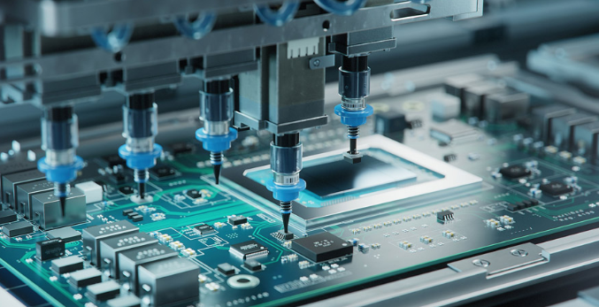
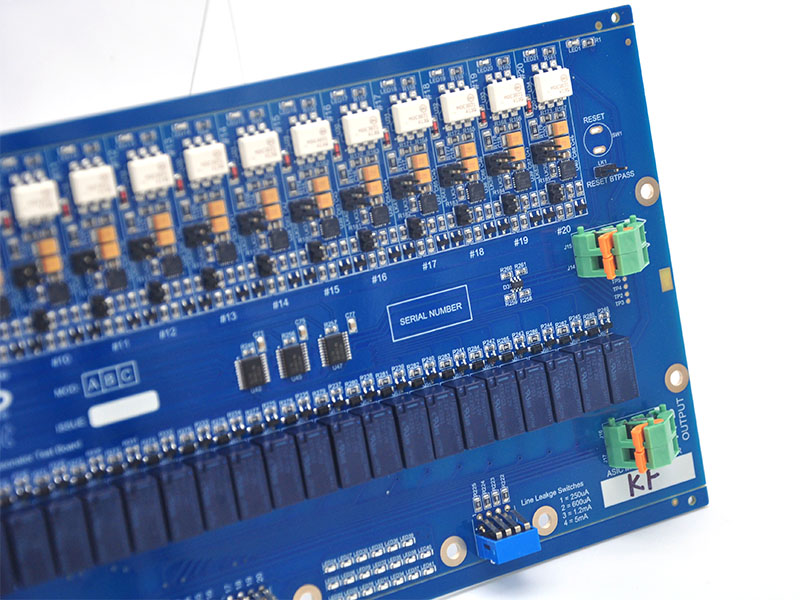
Assembly Capability and Precision
- High-speed SMT capacity reaching up to 13.2 million components per day, supporting both prototype and volume production.
- Flexible board size handling from 0.2 × 0.2 inches up to 20 × 20 inches or 22 × 47.5 inches.
- Advanced assembly precision supporting 01005 SMD components, 0.25 mm BGA pitch, and SMT, THT, or mixed-technology assembly.
- Full compatibility with reel, cut tape, tube, tray, and loose component packaging.
Quality Assurance System
- Inspection and testing conducted in accordance with IPC standards and customer-specific requirements.
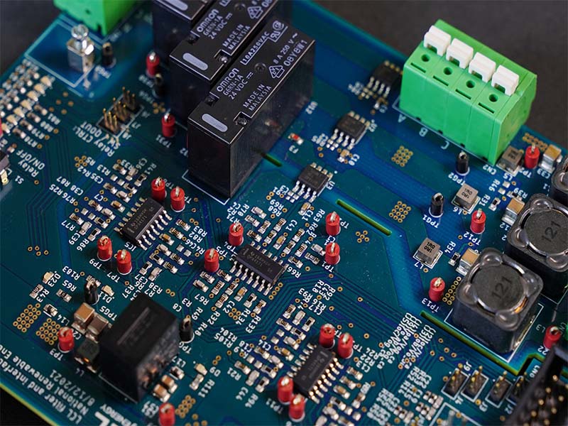
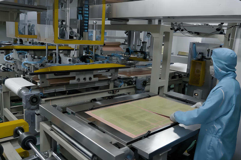
- End-to-end quality control including DFA review, incoming component inspection, AOI, X-ray inspection, functional testing, final inspection, and controlled cleaning and drying processes.
- Deployment of advanced equipment such as GKG-GLS solder paste printers, Yamaha YSM20R placement machines, and nitrogen reflow ovens to ensure consistency, accuracy, and yield stability.
Fast Turnaround and Delivery Control
- Standard delivery lead time of 1–5 days, with expedited options supporting shipment within 24 hours when required.
- Real-time WIP updates and production visibility, enabling customers to monitor project progress throughout the build cycle.
Manufacturing Capabilities Supporting Full Turnkey PCB Assembly
| Capability Area | EBest Circuit (Best Technology) |
|---|---|
| PCB Materials | FR-4, MCPCB (metal core), ceramic, flex, high-frequency |
| Layer Count | 10–32 layers |
| Board Thickness | 0.15 mm – 8.0 mm |
| Line/Space | Inner layers 3/3 mil (1/2 oz), outer layers 3/3 mil (1 oz) |
| Surface Finishes | OSP, HASL, ENIG, Immersion Silver, ENEPIG |
| Monthly Capacity | 260,000 sq. ft., 1,000+ board types |
| Certifications | ISO 9001:2015, IATF 16949:2016 |
In summary, by combining broad turnkey coverage, high-precision assembly, disciplined quality control, and fast response capability, EBest Circuit (Best Technology) delivers clear advantages as a full turnkey PCB assembly manufacturer in China. Its mature supply-chain integration, flexible manufacturing capacity, and internationally recognized quality systems make it particularly suitable for global customers seeking both cost efficiency and long-term reliability in turnkey PCBA projects.
To conclude, full turnkey PCB assembly provides a streamlined, accountable manufacturing model that simplifies supply-chain management and reduces project risk. This article explained how turnkey services work, how manufacturers differ, and what factors influence cost and reliability. By working with an experienced full turnkey PCB assembly manufacturer in China, customers can accelerate development, improve quality control, and achieve more predictable outcomes.
For project inquiries or a PCB assembly quote, please contact us via sales@bestpcbs.com.
FAQ About Full Turnkey PCB Assembly
Is full turnkey PCB assembly suitable for low-volume or prototype projects?
Yes. Full turnkey is widely used for prototypes and low-volume builds where coordination and speed are critical.
Who owns component quality in a full turnkey PCB assembly project?
In full turnkey projects, the manufacturer is responsible for component sourcing and quality assurance.
Can full turnkey PCB assembly support complex or high-mix designs?
Yes. High-mix, complex designs often benefit the most from turnkey services due to integrated engineering and sourcing.
What files are required to start a full turnkey PCB assembly order?
Typically required files include Gerber data, BOM, pick-and-place files, assembly drawings, and testing requirements.