pcb
Home > Blog

Posts Tagged ‘PCB’

Let you know about PCB copper layer thickness
星期五, 16 8 月, 2024

In the printed circuit board industry, the most common way to express the copper layer thickness on a PCB is in ounces (oz). 1oz means 1oz of copper evenly covers an area of 1 square foot, which is about 1.4mil. It uses the weight of the tissue area to express the average thickness of the copper foil. Expressed in terms of formula, 1oz=28.35g/FT2 (FT2 is square feet, 1 square foot = 0.09290304 square meters).

What is the standard thickness of a copper layer on a PCB?

In the manufacture of printed circuit boards (PCBs), the thickness of the copper layer is an important parameter that directly affects the electrical performance and reliability of the circuit board. Depending on the application requirements, the thickness of the copper layer can vary within a certain range. Generally speaking, the conventional copper layer thickness is between 1-35μm, with 35μm being the most commonly used thickness. For some applications with high reliability requirements, the copper layer thickness may reach more than 50μm.

The selection of the thickness of the copper layer is a decision-making process that takes into account a variety of factors, including the conductivity, heat dissipation, mechanical strength, cost and manufacturing difficulty of the circuit board. A larger copper thickness can reduce resistance and improve the conductivity and heat dissipation of the circuit board, but it will also increase material costs and production difficulties. Therefore, when designing PCB boards, engineers need to select a suitable copper thickness standard range based on specific application scenarios and design requirements to ensure the performance and reliability of the circuit board.

1oz copper thickness in mm = 0.035mm

0.5 oz copper thickness in mm = 0.0175mm

1.5 oz copper thickness in mils = 0.0525mm

2 oz copper thickness in mils =  0.07mm‌

How thick is PCB copper after plating?

PCB printed circuit boards are usually bonded to glass epoxy substrates with a layer of copper foil, usually 18, 35, 55 and 70 microns thick. The most commonly used copper foil is 35 microns thick.

The copper foil used by PCB manufacturers is generally 35~50 microns thick, and some are thinner than this, such as 10 microns, 18 microns, and thicker such as 70 microns. The thickness of the composite copper foil on a 1~3 mm thick substrate is about 35 microns. The thickness of the composite copper foil on a substrate with a thickness of less than 1MM is about 18 microns, and the thickness of the composite copper foil on a substrate with a thickness of more than 5 mm is about 55 microns.

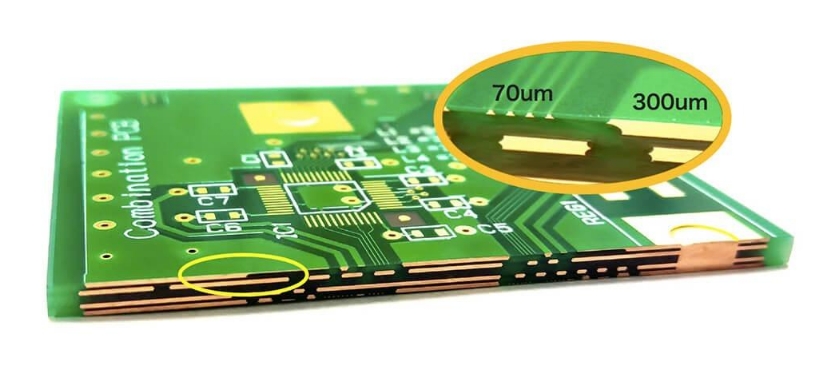
The copper layer thickness of PCB (printed circuit board) can be adjusted according to different needs and designs. Common copper layer thicknesses include 1oz (35μm), 2oz (70μm), 3oz (105μm), and other thicker options. For most applications, a copper layer thickness of 1oz is sufficient and suitable for general signal transmission. ‌For circuit boards that need to carry large currents, such as switching power supplies, a copper layer thickness of 2oz or higher is usually used. ‌In addition, there are some special cases where manufacturers provide extremely heavy copper up to 20 oz/ft2 (26.8 mils or 0.34 mm) to meet special needs. ‌

When choosing the thickness of the copper layer, factors such as the purpose of the circuit board and the magnitude of the signal voltage and current need to be considered. ‌For example, for circuit boards that require excessive current, a copper thickness of 70μm or 105μm may be used. ‌For thin laminates that require ultra-high density patterns, a copper thickness of 12μm may be used. ‌Therefore, the specific thickness of the PCB after copper plating is determined according to design requirements and specific applications.‌

How thick is 2 oz copper for PCB?

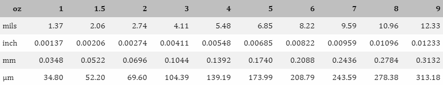
If 1 ounce (28.35 grams) of copper were flattened to evenly cover a surface area of 1 square foot (0.093 square meters), the resulting thickness would be 1.37mils (0.0348mm). A conversion chart for different units of measurement can be found below.

PCB copper layer thickness 

What is the difference between different copper thicknesses in PCB?

‌Copper is an excellent conductive material, and the thickness of the copper layer directly affects the conductive effect of the circuit board. ‌Thicker copper layers can provide lower resistance, reduce signal transmission losses, and are particularly suitable for high-frequency and high-speed digital circuits. ‌

During the operation of electronic equipment, good heat dissipation is a key factor in ensuring the performance and life of components. ‌Thicker copper layers can conduct and dissipate heat more effectively, preventing components from overheating. ‌

In high-power electronic devices, thicker copper layers can carry larger currents, avoiding burnout or performance degradation caused by excessive current.

Below is the conductivity corresponding to different copper thicknesses.

PCB copper layer thickness 

How thick is high current PCB copper?

In PCB design, copper thickness (also called copper thickness) is an important parameter, which directly affects the performance indicators of the circuit board such as current carrying capacity, heat dissipation and reliability. For PCBs that need to withstand high currents, such as high-power LED light strips, power circuit boards, high-power motor control boards or high-power inverter control boards, thicker copper layers are usually used to increase current carrying capacity.

PCB copper layer thickness 

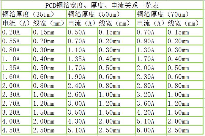
Different uses have different copper foil thicknesses. Common 0.5oz, 1oz, and 2oz are mostly used in consumer and communication products. Thick copper products above 3oz are mostly used for high currents, such as high-voltage products and power boards.

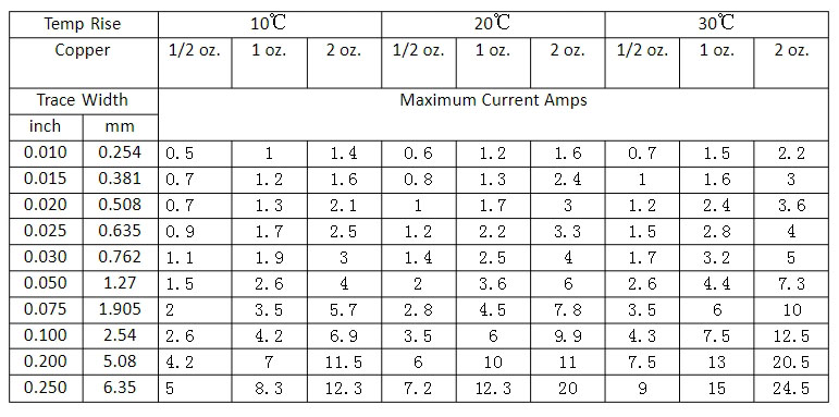
The thickness of copper foil (track width) will affect the current size. Although there is a formula that can directly calculate the maximum current carrying capacity of copper foil, it is not so simple when actually designing the circuit. Therefore, the safety factor should be fully considered during the design.

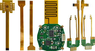
How thick is the copper in a flex PCB?

The thickness of copper foil in flexible PCB is generally 18μm, 35μm, 55μm and 70μm. These thickness specifications are suitable for different types of circuit board requirements, among which 35μm is the most commonly used copper foil thickness.

PCB copper layer thickness 

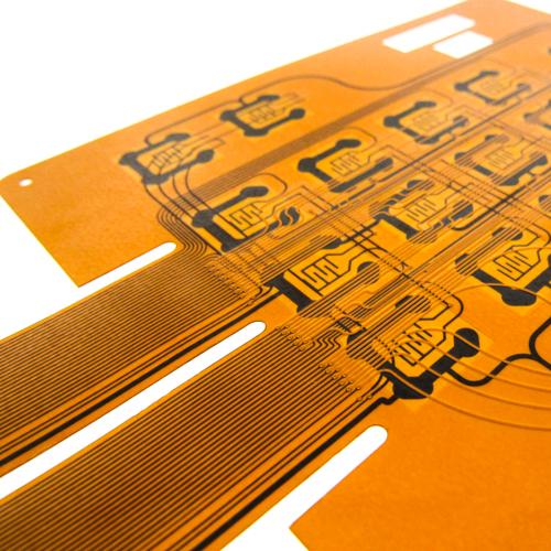
For flexible PCB, the choice of copper foil thickness depends on the specific purpose of the circuit board and the size of the signal voltage and current. For example, for PCBs that require excessive current, some parts will use 70μm copper thickness, while for signal transmission, 1oz (35μm) thickness is usually sufficient. In addition, for substrates of different thicknesses, the thickness of copper foil is also different. For example, the thickness of the composite copper foil on a 1mm thick substrate is about 18μm, and on a substrate thicker than 5mm, the thickness of the composite copper foil is about 55μm.

Conclusion:

PCBs for different usage scenarios correspond to different thicknesses of copper, and its thickness directly affects the conductive effect of the circuit board. If the copper layer is too thin, the conductivity may decrease, resulting in signal transmission attenuation or current instability. If the copper layer is too thick, although the conductivity will be very good, it will increase the cost and weight of the circuit board and easily lead to serious glue flow. In PCB manufacturing, it is necessary to select the appropriate copper thickness according to the design requirements and actual applications of the circuit board to achieve the best conductive effect.

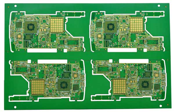
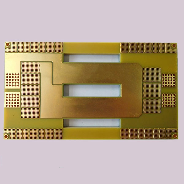
BEST Technology is a professional PCB circuit board manufacturer with a large area of site and equipped with useful and experienced production personnel. Corresponding to different thicknesses of copper, we have rich production and processing experience. We can meet the requirements of any circuit board copper layer thickness.‌

hdi printed circuit board,hdi pcb manufacturer
星期三, 14 8 月, 2024

What is hdi pcb?

HDI stands for High Density Interconnect, which refers to high-density interconnect technology. HDI circuit board is a high-end printed circuit board with very high circuit density and complexity, which can achieve high-speed signal transmission and reliability design. The main features of HDI circuit board are multi-layer circuit, thin plate, small aperture, dense wiring and fine circuit. It is widely used in mobile phones, computers, network communications, automotive electronics and other fields. Bestpcb is a professional HDI manufacturer with 18 years of HDI manufacturing experience.

What are the advantages of hdi pcb

  1. Higher line density: HDI PCB can support more circuit tracks, arrange more electronic components in a limited space, and achieve high-density interconnection.
  2. Smaller device spacing: The micro-hole technology of HDI PCB allows smaller spacing between components, which is suitable for compact design.
  3. Improve signal integrity: The advanced stacking layer structure is adopted to provide better signal transmission quality and reduce signal interference.
  4. Improve reliability: The manufacturing process of HDI PCB improves the mechanical strength of the board, making it more durable and suitable for demanding application environments.
  5. Improve circuit integration: More line connections and component arrangements are achieved in a limited circuit board space to meet the needs of modern products that are thin and compact.
  6. Enhance signal transmission efficiency: The use of advanced wires and connection methods can increase the operating speed of electronic devices and reduce energy consumption.
  7. Support more complex system design: High-density connection capabilities provide support for complex system design and give full play to the performance of electronic devices. ‌
  8. Promote innovation in the electronics industry: The application of HDI technology has promoted the innovation and development of the electronics industry, making electronic equipment more intelligent and efficient. ‌
  9. Smaller size: It can complete a large number of circuit connections in a smaller space, meeting the needs of electronic products for lightness and portability. ‌
  10. Higher signal transmission speed: The high-density line design allows signals to be transmitted quickly in a short time, improving the system operation speed and response speed.

Why does HDI PCB need via filling and plating?

‌Via filling plating plays a vital role in ‌HDI PCB manufacturing, with the main purpose of improving ‌electrical performance, connection reliability, operating frequency, and avoiding electromagnetic interference. This technology fills the blind holes of HDI PCB with conductive materials through the electroplating process to form a conductive path, which improves the performance and reliability of electronic equipment.

  1. Improve electrical performance: Via filling plating can improve the electrical performance of HDI PCB, especially in high-frequency circuit board design, which is crucial for improving connection reliability, operating frequency and avoiding electromagnetic interference.
  2. Via plugging and electrical interconnection in one step: Via filling plating technology combines via plugging and electrical interconnection, avoiding the defects caused by resin via filling, and also avoiding the CTE difference caused by other materials via filling.
  3. Improve efficiency: Compared with resin via filling or other materials via filling, via filling plating has a simpler process and higher efficiency.
  4. Process flow and technical challenges of via filling plating
  5. Process flow: including steps such as tank preparation, setting of electroplating process control parameters, and analysis of potion addition.
  6. Technical challenges: including positioning accuracy issues and electroplating quality issues, which need to be solved by strictly controlling parameters such as electroplating time and current density.

Application scenarios of hole filling electroplating

First-order HDI: Suitable for electronic devices with less complex circuits.
Second-order and above blind hole electroplating copper filling: Suitable for more complex electronic devices, such as mobile phones, laptops, etc.
Comparison between hole filling electroplating and full-board electroplating
Full-board electroplating: Although it can provide a uniform surface copper thickness distribution, it may encounter the problem of residual dry film on the board surface or in the hole during pre-treatment, resulting in some areas unable to be plated with copper. In addition, the etching process after full-board electroplating may cause quality defects such as side etching and fine lines.
Hole filling electroplating: Compared with full-board electroplating, hole filling electroplating is more accurate in filling blind holes, avoiding the problems that may be encountered in full-board electroplating, while simplifying the process and improving efficiency.

Materials of HDI PCB

The materials of HDI PCB mainly include coated copper foil (RCC), prepreg, copper foil, etc.

Resin-coated copper foil (RCC): This is a material that coats a special resin film layer on electroplated copper foil, used for HDI insulation layer. The characteristics of RCC include no glass dielectric layer, easy laser and plasma micro-hole forming, extremely high peel strength and good toughness, suitable for micro-narrow line etching. Laser drilling is performed on RCC, and the aperture shape formed is an inverted trapezoid, and the general aperture size is 0.076-0.10 mm. The use of RCC makes HDI PCB more widely used in small portable products, such as mobile phones, digital cameras, laptops, etc.

Prepreg and copper foil: These are basic materials in HDI PCB manufacturing, there are no special requirements, and they are suitable for different types of HDI PCB structures. The inner layer circuits are generally 1 ounce copper thick, while the outer layer circuits are plated with half an ounce of base copper to 1 ounce of finished copper thickness. The thickness of the board is usually thinner to meet the miniaturization requirements of HDI PCB.

Other materials: In addition to the main materials mentioned above, the manufacture of HDI PCBs may also involve other materials, such as FR4, PI (polyimide), BT, etc. These materials are selected according to specific application requirements. For example, FR4 has good electrical and mechanical properties and is suitable for most general applications; PI has higher heat resistance and chemical corrosion resistance, and is suitable for high temperature, high humidity and strong acid and alkali environments, but it is more expensive and difficult to process; BT combines good electrical properties, mechanical properties and thermal stability, and is suitable for application scenarios that require higher heat resistance.

Classification of HDI circuit boards

HDI circuit boards are mainly divided into first-order, second-order, third-order, high-order (including fourth-order and above) and Anylayer HDI. ‌

  1. First-order HDI circuit boards mainly include single-sided or double-sided micro-hole processes, and the circuit layer has only one layer. ‌This type of HDI circuit board is suitable for applications with high requirements on cost and space, such as consumer electronics. ‌
  2. Second-order HDI circuit boards contain two circuit layers, which are more complex but also more powerful than first-order HDI circuit boards. They can handle higher signal frequencies and are suitable for applications that require high performance, such as high-end communication equipment and computer hardware. ‌
  3. Third-order HDI circuit boards contain three circuit layers. They are the most complex type at present. They can handle the highest signal frequency and the maximum data transmission rate. They are usually used in applications that require the highest performance, such as aerospace and military equipment. ‌
  4. High-order HDI (including fourth-order and above) The applications of third-order or fourth-order HDI in electronic terminal products are more, while those above fourth-order are mostly converted to Anylayer structure. ‌
  5. Anylayer HDI refers to HDI of any order/any layer. Compared with PCB boards with traditional lamination processes, HDI can reduce costs to a lower level when the stacking density exceeds eight layers. It also has higher electrical performance and signal accuracy, and significantly improves the performance of electromagnetic waves and radio frequency interference, electrostatic discharge and heat conduction in interconnection and relay transmission.

HDI PCB Process Flow

The process flow standards of HDI PCB mainly involve the application and processing technology of high-density interconnection technology (High Density Interconnection Technology, HDI for short), including first-order, second-order and third-order processes. Specifically, the HDI PCB process flow includes the following key steps and characteristics:

First-order process (1+N+1): This is a basic high-density interconnection technology that manufactures multi-layer boards through build-up and micro-blind via technology.

Second-order process (2+N+2): Further development on the basic technology, adding more layers and complexity.

Third-order process (3+N+3): Represents the highest stage of HDI technology, with extremely high layers and interconnection density

Differences between HDI PCB and ordinary PCBs

  1. Differences in circuit design:
    HDI PCB adopts a more sophisticated circuit design, with smaller line width and spacing, and smaller aperture, which can integrate more electronic components and realize more complex circuit functions. ‌
    The blind, buried and stacked hole designs of HDI PCB greatly improve the utilization rate and signal transmission performance of the circuit board.
  2. Differences in manufacturing process:
    The manufacturing process of HDI PCB is more complicated, requiring high-precision processes such as laser drilling technology, hole filling electroplating technology and photolithography technology.
    The manufacturing cost of HDI PCB is relatively high, but the performance and reliability are also higher. ‌
  3. Differences in application:
    Due to its high density and high performance, HDI PCB is widely used in high-end electronic products, such as smartphones, tablets, high-end communication equipment, etc.
    Ordinary PCB is mainly used in low-end electronic products and general electronic equipment.
  4. Characteristics and application scenarios of HDI PCB:
    HDI PCB has high-density wiring, multi-layer structure, high-precision manufacturing process and excellent electrical performance, which can meet the extremely high requirements of high-end electronic products for size, weight, performance and reliability.
    HDI PCB is widely used in smart phones, tablet computers, high-end communication equipment and other fields, promoting the continuous development and upgrading of electronic products.

Application of HDI PCB

HDI PCB (High Density Interconnection Printed Circuit Board) is widely used in multiple industries, including medical equipment, mobile phones, laptops, automotive electronics, computer industry, and future 5G technology fields

  1. Medical equipment: The application of HDI PCB in medical equipment, such as sphygmomanometers and ultrasonic imaging systems, achieves accurate measurement of blood pressure and high-definition imaging of the internal structure of the body, providing patients with timely and accurate diagnosis and treatment information. ‌
  2. Mobile phone industry: With the increasingly miniaturized design of mobile phones, HDI PCB is widely used in transceiver modules, motherboards, SIM card interfaces, fingerprint recognition modules and other parts of mobile phones due to its high density, high quality and high reliability. ‌
  3. Computer industry: In the computer industry, the application of HDI PCB improves the performance of computers, especially in the fields of high-speed algorithms and multimedia applications, and adapts to the miniaturization trend of computer equipment2. ‌
  4. Automotive electronics: HDI PCB has broad application prospects in the field of automotive electronics. In addition to the dominant mobile phone market, it also involves multiple fields such as automobiles, modules and artificial intelligence, demonstrating its key role in complex electronic systems. ‌
  5. Future development trends: With the advent of 5G technology, the demand for HDI PCB will continue to increase, requiring higher speeds and frequencies while adapting to smaller and thinner device designs. Research new micro HDI PCB boards to adapt to future development trends. ‌
What is the thickness of copper used in PCB manufacturing?
星期三, 14 8 月, 2024

PCB copper thickness is generally divided into 1OZ (35um), 2OZ (70um), 3OZ (105um), of course, there are thicker ones. The copper thickness depends on what kind of board you are making. For example, 2OZ is enough for switching power supplies with high current, and 1OZ is enough for general signals.
Generally, double-sided boards are 1oz
Multi-layer boards are generally 1/2oz 1/3oz for the inner layer and 1oz 1/2oz 1/3oz for the outer layer

0.5 oz copper thickness About 0.685 mm.
1 ounce is about 1.37 mm, so 1.37÷2=0.685,
0.5 oz copper thickness in mm About 0.685 mm

1 oz copper thickness: This is the most common and basic copper thickness standard, also known as standard copper thickness. 1 oz copper thickness refers to the weight of 1 ounce (about 35.3 grams) of copper foil per square foot of board area, and the corresponding copper foil thickness is about 1.4 mils (0.035mm). This copper thickness is suitable for most common circuit board designs and applications.

2 oz copper thickness: 2 oz copper thickness refers to the weight of 2 ounces (about 70.6 grams) of copper foil per square foot of board area, and the corresponding copper foil thickness is about 2.8 mils (0.071mm). This copper thickness is suitable for some applications that require higher current carrying capacity, such as power electronic devices and high-power LEDs.

3 oz copper thickness: 3 oz copper thickness refers to the weight of 3 ounces (about 105.9 grams) of copper foil per square foot of board area, and the corresponding copper foil thickness is about 4.2 mils (0.107mm). This copper thickness is suitable for some special applications that require higher current carrying capacity, such as high-power amplifiers and high-power power supplies.

PCB copper foil thickness standard

  1. Common international PCB thicknesses are: 35um, 50um, and 70um.
  2. The copper foil (copper cladding) thickness of general single-sided and double-sided PCBs is about 35um (1.4mil), and the other specifications are 50um and 70um.
  3. The surface thickness of multilayer boards is generally 35um=1oz (1.4mil), and the inner layer is 17.5um (0.7mil).

The relationship between the line width, copper thickness and current passing through the PCB board

1 foot = 12 inches
1 inch = 1000 mil
1mil = 25.4um
1mil = 1000uin mil is sometimes called inch
1um = 40uin (some companies call microinches “microinches”, which are actually microinches)
1OZ = 28.35 grams per square foot = 35 microns

The relationship between the line width, copper thickness and current passing through the PCB board

PCB copper thickness current comparison table

Copper foil width Copper foil thickness
70um 50um 35um
2.50mm 6.00A 5.10A 4.50A
2.00mm 5.10A 4.30A 4.00A
1.50mm 4.20A 3.50A 3.20A
1.20mm 3.60A 3.00A 2.70A
1.00mm 3.20A 2.60A 2.30A
0.80mm 2.80A 2.40A 2.00A
0.60mm 2.30A 1.90A 1.60A
0.50mm 2.00A 1.70A 1.35A
0.40mm 1.70A 1.35A 1.10A
0.30mm 1.30A 1.10A 0.80A
0.20mm 0.90A 0.70A 0.55A
0.15mm 0.70A 0.50A 0.20A

PCB copper thickness current comparison table

PCB copper content

The copper content of PCB copper foil is generally 90% and 88%.

Copper foil is made of copper and a certain proportion of other metals. There are two common specifications of copper foil, namely 90% and 88% copper content. The size of these two specifications of copper foil is 16*16cm, which is widely used in various occasions where copper foil is needed, including PCB manufacturing. In PCB manufacturing, copper foil is the basic material of the circuit board, and its thickness and copper content have an important influence on the electrical performance and durability of the circuit board. The thickness of copper foil is usually expressed in OZ (ounces). The standard PCB copper thickness range is 1/4OZ-6OZ. The specific thickness includes 1OZ, 2OZ, 3OZ, 4OZ, 5OZ, 6OZ, which correspond to different copper thickness sizes, such as 35um, 70um, 105um, 140um, 175um, 210um. In practical applications, the commonly used copper thicknesses are 1OZ, 2OZ, 3OZ, 4OZ, etc. These copper thicknesses can meet the needs of most electronic products.

The copper content of PCB copper foil is generally 90% and 88%.

Why is the copper foil on the surface of PCB copper+plating?

The copper foil on the surface of the PCB adopts the copper+plating method, mainly because this treatment method can provide better conductivity and protection circuit. ‌Copper foil is the conductor of PCB, and its basic material is copper, while plating (plating) is a layer of metal added on the basis of copper foil by electroplating or other methods, usually tin, gold or other alloys, to provide additional protection and enhance electrical performance. ‌The reasons and advantages of this treatment method are as follows: ‌

  1. Conductivity: Copper has good conductivity and is an ideal medium for the flow of electrons. ‌In PCB, copper foil is used as a conductive layer to connect various electronic components and ensure smooth transmission of current. ‌
  2. Protective circuit: By adding plating, such as tin or gold, to the copper foil, additional protection can be provided to prevent the copper foil from being oxidized or corroded, thereby protecting the long-term stability and reliability of the circuit board. ‌
  3. Enhanced electrical performance: Plating not only prevents copper foil from being oxidized, but also enhances electrical performance by selecting appropriate plating materials, such as using gold plating to improve the corrosion resistance and conductivity of the circuit board. ‌
  4. Cost considerations: Although gold is an expensive metal, the use of gold plating in certain key signal lines or high-density interconnection areas can significantly improve the performance and reliability of the circuit board, especially in reducing signal loss and interference in high-frequency signal transmission.
Rigid flex pcb Design & Prototype Right the First Time
星期一, 12 8 月, 2024

rigid-flex printed circuit board ,Rigid flex pcb manufacturer. More than 5 years design team of 10 people. Quick proofing within 1 week. A 3,000-square-meter factory for small batch to mass production and assembly.

What is a rigid flex pcb?

Rigid flex pcb,rigid-flex printed circuit board,Rigid flex circuit are a hybrid construction flex circuit consisting of rigid and flexible substrates which are laminated together into a single structure. Each layer of rigid-flex circuit are electrically interconnected by plated through holes (PTH), which is different from a flexible circuit with FR4/PI stiffener on top or bottom of flex circuit only by the means of presensive or thermal senstive adhesive only, no PTH.

What is a rigid flex pcb?

Rigid-flex PCBs can be divided into single-sided boards, double-sided boards and multi-layer boards according to the number of conductive circuit layers. Multi-layer boards usually contain multiple rigid layers and flexible layers, and the circuits are connected and interconnected through interlayer connections.

Is Rigid flex PCB reliable?

  1. Design and manufacturing efficiency: Designers of rigid-flex boards can use a single component to replace a composite printed circuit board connected by multiple connectors, multiple cables and ribbon cables, which not only has stronger performance and higher stability, but also limits the scope of the design to one component, optimizing the available space by bending and folding the lines like a stacked paper swan.
  2. Space and weight optimization: In PCB prototyping for consumer electronics, the use of rigid-flex boards not only maximizes space use and minimizes weight, but also greatly improves reliability, eliminating many needs for solder joints and fragile and fragile wiring that are prone to connection problems. The design of this circuit board allows the size and weight of equipment and systems to be reduced while maintaining functionality.
  3. High stress environment adaptability: Rigid-flex boards also have high impact resistance and can survive in high stress environments, which makes it widely used in military, aviation and medical equipment.
  4. Excellent electrical performance: Rigid-flex boards provide excellent electrical performance, and good thermal conductivity makes components easy to cool. The lower dielectric constant of the flexible part allows for fast transmission of electrical signals, and the PI substrate has a higher glass transition temperature or melting point, which allows the components to operate well at higher temperatures.
  5. Assembly reliability: Rigid-flex boards reduce the hardware required for traditional rigid boards and flexible boards to be connected, such as traditional jumper sockets, etc., and can provide higher assembly reliability.

What is the difference between rigid flex and semi flex?

  1. Definition and structure
    Rigid-flexible board: It is a combination of soft board and hard board, that is, a thin layer of flexible bottom layer and rigid bottom layer are combined and laminated into a single component to form a circuit board1. It changes the traditional flat design concept and expands it to a three-dimensional space concept. It has both rigid layer and flexible layer and is a multi-layer printed circuit board.
    Semi-flexible board: It is a PCB used in the field of static bending obtained by combining controlled deep milling or rigid-flexible board processing technology (such as milling cover or opening window, etc.) in the standard hard board processing process2. It often uses FR4 material, first processes the PCB according to the normal process, and then mills the middle part that needs to be bent to make it flexible.
  2. Flexibility and application
    Rigid-flexible board: It has higher flexibility and can be bent, folded or rounded, and then integrated into various products, such as aerospace equipment, military aircraft, high-end medical equipment, digital cameras, portable cameras and high-quality MP3 players. ‌
    Semi-flexible board: Although it can be bent or curved, its flexibility is not as good as that of rigid-flexible board. It is mainly used in situations where static bending is required, such as endoscopes in medical equipment, injection needle tip protection circuit boards, and medical equipment temperature control circuit boards. ‌
  3. Processing and cost
    Rigid-flexible board: Due to the mixed use of multiple materials and multiple production steps, its processing time is longer and the production cost is higher. ‌
    Semi-flexible board: Although its processing process is also more complicated, its processing cost is lower than that of rigid-flexible board, and it is more suitable in some applications. ‌
  4. Features and advantages
    Rigid-flexible board: It has stronger performance and higher stability, can reduce space and weight, and improve the reliability of connection. ‌
  5. Semi-flexible board: It has the advantages of low cost, good dimensional stability, bendable three-dimensional installation to reduce space, and reduce the number of interfaces during assembly to improve reliability.‌

how do they add rigid layers to flex pcb?

  1. Design layout: Before starting the manufacturing process, the PCB design layout is first carried out to determine the location and connection method of the components. ‌
  2. Substrate preparation: Clean the laminate containing the copper layer to prepare for the subsequent manufacturing process. ‌
  3. Pattern generation: The generation of circuit patterns is completed by screen printing or photo imaging. ‌
  4. Etching process: The laminate with the circuit pattern is soaked in an etching tank or sprayed with an etchant solution for etching. ‌
  5. Mechanical drilling: Circuit holes, pads and via patterns are drilled using a precision drilling system or technology, such as laser drilling technology. ‌
  6. Copper plating process: Deposit the required copper in the plated vias to establish electrical interconnections between layers. ‌
  7. Covering layer application and lamination: Apply the covering layer material (such as polyimide film) and adhesive, and laminate under specific temperature, pressure and vacuum limits to ensure proper adhesion of the covering layer. ‌
  8. Apply stiffeners: Apply local additional stiffeners before additional lamination processes as required by the board design. ‌
  9. Flexible board cutting: Cut flexible boards from production panels using hydraulic punching methods or specialized punching knives. ‌
  10. Electrical testing and verification: Conduct electrical testing in accordance with IPC-ET-652 guidelines to confirm that the insulation, connection, quality, and performance of the circuit board meet the requirements of the design specifications.

What are the disadvantages of rigid flex PCB?

  1. Material damage or breakage: The flexible materials used in rigid-flex boards are susceptible to flexure and bending. Long-term use or improper handling may cause damage or breakage of the flexible part, resulting in an open circuit.
  2. Poor welding: The manufacture of rigid-flex boards requires welding processes. If the welding is poor or the solder joints are of poor quality, it may cause loose connections or solder joints to fall off, resulting in an open circuit.
  3. Excessive bending or stretching: Excessive bending or stretching during use may cause the connection wires or wires of the flexible part to be stretched excessively and break, causing an open circuit.
  4. Design defects: If the design of the rigid-flex board is unreasonable or defective, such as insufficient design of the overbending area or too small bending radius, the material of the flexible part may be damaged by excessive stress, resulting in an open circuit.
  5. Environmental factors: Under different environmental conditions, it may be affected by factors such as temperature, humidity, and chemicals. Long-term use in harsh environments may cause material aging or corrosion, resulting in an open circuit. ‌
  6. Damage during assembly: During the assembly process, improper operation or external force may cause damage to the connecting wires or wires of the flexible part, resulting in an open circuit.

Application fields of rigid flex PCB

  1. Automotive electronics: Rigid-flex boards are widely used in automotive electronic systems such as dashboards, navigation systems, and in-car entertainment systems in the automotive industry. Their flexibility and high reliability enable them to adapt to the complex spatial layout and vibration environment inside the car.
  2. Medical equipment: In the field of medical equipment, rigid-flex boards also have important applications, such as medical monitoring equipment, medical imaging equipment, etc. Its flexible part can adapt to different equipment shapes and size requirements, while having stable circuit connection performance.
  3. Aerospace field: Rigid-flex boards are usually used in aircraft dashboards, navigation systems, communication equipment, etc. in the aerospace field. Due to their light, thin and flexible characteristics, rigid-flex boards have become an ideal choice for aerospace equipment.
  4. Smart wearable devices: With the rapid development of smart wearable devices, rigid-flex boards are widely used in products such as smart watches and health monitoring equipment. They can be combined with curved display screens, sensors and other components to achieve a more humanized design.
  5. Industrial control field: In the field of industrial automation control, rigid-flex boards are often used in PLC controllers, robot control systems, sensor interfaces, etc. Its flexibility and reliability ensure the stable operation of the equipment in harsh environments.
Application fields of rigid flex PCB

Rigid flex pcb manufacturer

rigid flex pcb.rigid-flex printed circuit board,Rigid flex circuit are a hybrid construction flex circuit consisting of rigid and flexible substrates which are laminated together into a single structure. Each layer of rigid-flex circuit are electrically interconnected by plated through holes (PTH), which is different from a flexible circuit with FR4/PI stiffener on top or bottom of flex circuit only by the means of presensive or thermal senstive adhesive only, no PTH.

Rigid flex pcb manufacturer

Multilayer circuitry-from 3 to 14+ layers
Min LW/LS: 4mil/4mil
Adhesive-based and adhesiveless constructions, including thermoplastic and thermoset stiffener attachment.
Polyimide substrates: 1/2mil – 4mil
Copper: 1/3OZ – 2OZ, RA or ED type
Stiffeners include Polyimide (0.075-0.20mm), FR4 (0.15-2.0mm), and punched or formed metal parts (0.075-1.0mm)
Low-cost, conventional fabrication and lamination completed with PTH based plating
Screened inks, photo-imageable soldermasks, or laminated coverlay dielectrics
Surface finishes: ENIG, electroplated nickel/gold, immersion silver, tin,
EMI Shielding

how to design flex rigid pcb?

Rigid-Flex Circuit Design Guidelines

To form a rigid-flex, follow these considerations to ensure the best results.

Considerations When Designing Rigid-Flex Circuits

To produce a rigid-flex PCB with unmatched quality and functionality, you must follow the correct manufacturing specifications. This is the set guidelines and standards that manufacturers must consider when designing and manufacturing flexible circuit boards.

Determine Manufacturing Process and Materials Beforehand

Depending on the flexibility you require, you need to decide beforehand what materials to use and the methods to use. Example; When the board you are designing only needs to be folded during manufacturing and thereafter be in a fixed position without bending, you can decide the following

  1. Copper type and grade
  2. Manufacturing method
  3. Number of layers to be used.

On the other hand, if the board is for an application with frequent movement, vibration, and impact, you must be clear in choosing the following:

  1. Copper Coils
  2. Adhesives and
  3. Number of Layers

Place Copper Traces at Right Angles to Rigid-Flex

Copperworks is a great fit when placed on the right edge of the board. Avoid bending copper traces at corners as it will pull stress and may not create the best bend. For PCB flex that requires bending, use sharp radius bends to avoid smudging copper traces.

Provide adequate pad support for exposed copper

Repetitive stress from frequent bending can cause copper on the circuit to break away from the polyimide substrate. Support exposed copper with pads to prevent separation.

Use hatched polygons

Hatched polygons instead of solidified copper help maintain the flexibility of flexible PCBs.

Leave at least 1/2mm gap between copper ring and adjacent vias

1/2mm helps avoid fatigue caused by frequent bending. Placing vias in fixed areas of the board helps avoid frequent movement and bending, resulting in the best rigid-flex.

What is Tda7294 amplifier board &tda7294 datasheet
星期三, 7 8 月, 2024

TDA7294 is a class AB monolithic audio amplifier integrated circuit launched by SGS-THOMSON Microelectronics in the 1990s. It swept away the raw, cold and hard sound of previous linear integrated amplifiers and thick film integrated amplifiers, and is widely used in HiFi fields, such as home theaters, active speakers, high-performance TVs and other fields.

The chip adopts a 15-pin dual-row asymmetric plug-in package, the differential input stage is composed of bipolar transistors, and the driver stage and power output stage use DMOS field-effect transistor semiconductor technology. This hybrid semiconductor manufacturing process allows TDA7294 to take into account the advantages of bipolar signal processing circuits and MOS power tubes, and the playback sound is very friendly (it is praised by audiophiles as a “tube-flavored amplifier”); the built-in silent standby function, short-circuit current and overheating protection functions make its performance more perfect. It can be used in HiFi home audio, active audio, high-performance TVs and other fields.

Tda7294 amplifier board

tda7294 amplifier board

tda7294 amplifier board PCBA

  1. This circuit is an official standard circuit, stable and reliable.
  2. The filter uses a large electrolytic capacitor with a withstand voltage of 50V and a capacity of 2200uf.
  3. Power supply voltage: dual 12-36V ring transformer, dual 32V ring transformer is recommended
  4. Output power: 85W*1 undistorted rated power, peak power 100W
  5. Can easily drive speakers above 100W, speaker impedance: 4-8 ohms
  6. PCB size: 50*50mm
tda7294 amplifier board

Basic parameters:
Power supply: dual 18-28V AC
Power: 2X80W+160W subwoofer
Circuit board size: 218x98MM
Potentiometer function: low frequency frequency adjustment, subwoofer volume. Left and right channel volume, treble, bass.

Adopting the new laser dark word TDA7294
The power filter uses 6 63V3300UF capacitors, and the rectifier uses a 25A imported rectifier flat bridge.
PCB uses 1.6mm thick double-sided board, 2.0 ounces copper thickness, and full tin spraying process to ensure good passing performance of large and small currents.
Fever component assembly, the subwoofer part consists of two new TDA7294 BTL output,
The low-pass filter is designed according to the frequency adjustable design of home theater style (50-150HZ), with strong power!
The left and right channels are served by two TDA7294 respectively, and the input coupling capacitor uses the German imported WIMA 2.2UF coupling capacitor, which makes the sound sweeter!
The signal-to-noise ratio of the board is also very high, and even if you put your ear close to the speaker, you can’t hear the AC noise! ​​It is the best choice for upgrading 2.1 amplifiers!

TDA7294 datasheet

TDA7294 datasheet
TDA7294 datasheet

TDA7294 Main Features

Wide supply voltage range: ±10V ~±40V
High output power: 70W (up to 100W)
Standby and mute functions
Noiseless ON/OFF switch
Low noise and low distortion
Short circuit protection and overheat protection

TDA7294

Pin function
Pin 1 is the standby terminal;
Pin 2 is the inverting input terminal;
Pin 3 is the positive input terminal;
Pin 4 is grounded;
Pins 5, 11, and 12 are empty pins;
Pin 6 is the bootstrap terminal;
Pin 7 is +Vs (signal processing part);
Pin 8 is -Vs (signal processing part);
Pin 9 is the standby pin;
Pin 10 is the mute pin;
Pin 13 is +Vs (final stage);
Pin 14 is the output terminal;
Pin 15 is -Vs (final stage)

DIY Production

1) The first step is to get the PCB. Here you can make the PCB yourself by DIY ironing method. Since the PCB is easy to make, the PCB design is kept single layer only, or you can get ready-made quality PCB from best.or custom tda7294 amplifier board.
2) After the PCB is completed, carefully mount all small components like jumpers, resistors, diodes, etc. to the PCB and trim their terminals, then solder them to the PCB first, because there are many components on this board, so it is better to solder them one by one
3) After installing the small components, install the large components like capacitors, fuse holders, rectifiers to the PCB and solder them. (Don’t install the power filter capacitor, 22000uF capacitor for now. Completed in the following steps)
4) After that, it’s time to mount all 7 ICs to the PCB and solder them.
5) Now properly mount the heat sink on the IC using insulating MICA and insulating plastic shoulder washers. Remember to use good quality thermal paste between the heat sink and IC.
6) After mounting the IC on the heat sink. Check the continuity between the heat sink and the IC back plate using a multimeter. There should not be any continuity between them. Please note the heat sink isolation
7) Now mount the cooling fan to the PCB using cable ties or any other suitable method.
The board assembly is now complete. Clean the track side of the board using IPA (Isopropyl Alcohol) or cleaning flux and then power the board using a 20-0-20 VAC transformer or a 24-0-24 VAC transformer.

Which one has better sound quality, TDA7294 or LM3886? Voltage AC 28v

LM3886 has better bass because its maximum current can reach 10A, which means it can drive a 2-ohm box without any problems. From the parameters alone, LM3886 is worse than 7294. And it is true in practice, especially for bass. If the transformer is OK, it feels very powerful. 7294 is not as good as 3886 in bass. The current is large when it comes to bass. 7294 itself has overcurrent protection. When the current reaches a certain level, it starts to limit the output current. However, 7294 is better in treble.

The origin of inches and how to convert millimeters to inches
星期三, 7 8 月, 2024

Inches to MM conversion

In the imperial system, 12 inches is 1 foot, and 36 inches is 1 yard.
1mil=1/1000inch=0.00254cm=0.0254mm.
1inch=2.54cm=25.4mm=1000mil
1 inch=2.54cm=25.4mm.

10 mm = 0.393700787 inches
50 mm =1.96850394 inches

1400mm in inches
1400 mm = 55.1181102 inches

1500 mm to inches
1500 mm = 59.0551181 inches

1800mm to inches
1800 mm =70.8661417 inches

Origin of the inch

The word “inch” comes from the Old English word “ynce”, which comes from the Latin word “uncia” (meaning “one twelfth”).
In the 14th century, King Edward II of England promulgated the “standard legal inch”; its regulations were: the length of the three largest grains of wheat selected from the middle of the barley ear and placed end to end in a row is 1 inch.

mm or inches in the PCB industry

(including the substrate and all copper layers, solder mask and silk screen), either millimeters or inches can be used as units. However, 1.6 mm is not the only choice, and the thickness of the PCB can vary depending on the specific application, ranging from 0.3 mm to 4.0 mm1.
In PCB design, for design and layout units such as traces, pads, spacing and grids, the imperial unit “thou” (one thousandth of an inch) should be used instead of millimeters. For mechanical manufacturing unit requirements such as apertures and PCB board sizes, millimeters can be used. This shows that when designing PCBs, you need to be familiar with the conversion relationship between the imperial unit “thou” and the metric unit millimeter. ‌
In summary, the units used in the PCB industry depend on the specific application scenarios and requirements. When describing the thickness of the PCB board, millimeters or inches can be used as units, while in design and layout, the imperial unit “thou” should be used to adapt to design requirements.

PCB package size

PCB length units usually refer to the shortest distance between components on the PCB. Common length units are inches, centimeters and millimeters. For example, the minimum PCB length unit for the 0805 package size is 1 inch, while the minimum PCB length unit for the 0402 package size is 0.25 inches. In addition, there are some other commonly used PCB package sizes, such as 0101 package size, 0201 package size, 0302 package size, etc.

PCB package size is a standard size for mounting and connecting electronic components on PCBs. The following are the most commonly used device PCB package sizes:
1.0805 package size: This package size is used for electronic components of 8 inches (about 20 cm) in size, including transistors, capacitors, inductors and other small components.
2.0402 package size: This package size is used for electronic components with a size of 4 inches (about 10 cm), including transistors, capacitors, inductors and small components.
3.0603 package size: This package size is used for electronic components with a size of 6 inches (about 15 cm), including transistors, capacitors, inductors and small components.
4.1206 package size: This package size is used for electronic components with a size of 12 inches (about 30 cm), including transistors, capacitors, inductors and small components.

The unit of PCB length is usually millimeter (mm) or inch (inch), while the unit of copper foil thickness is OZ (ounce), which is about 35um or 1.35mil. When designing the PCB of the op amp circuit, factors such as layout, wiring, power decoupling, and heat dissipation design need to be considered to ensure signal integrity and stability.

What is a 5.1 amplifier board?
星期三, 7 8 月, 2024

A 5.1 amplifier board is a sound amplifier that can expand the current and voltage of an audio signal to make the sound louder. In addition, a 5.1 amplifier board also has a multi-channel processing function, which can output audio signals through multiple channels to enhance the sound field effect, making listening to music, watching movies, etc. more three-dimensional and realistic.
Compared with traditional 0 and 1 amplifiers, in addition to being able to connect two front speakers and two rear speakers, a 5.1 amplifier board can also connect a center speaker and a subwoofer, making the bass of music or movies more prominent and the sound deeper.
5.1 amplifiers are widely used in home theater systems. By combining with projectors, TVs and other equipment, a theater environment with excellent audio-visual effects can be created. In addition, for music lovers, a 5.1 amplifier board is also an indispensable device that can not only maximize the effect of music, but also allow people to experience the charm of music in an immersive way.

What is a 5.1 amplifier board?

5.1 Basic parameters of the amplifier board

Working mode: Class D
Quiescent current: 50mA
Working efficiency: 90%
Rated output power: 2200W+400W Frequency response: 20Hz to 20KHz Working voltage: DC24V-42V( Recommended voltage: DC42V Maximum output current: 10A PCB size: 114109MM
Potentiometer center distance: 21.5MM 21.5MM 21.5MM from left to right
Original TPA3223 is used

TPA3223 2.1 Digital Bluetooth 5.1 3034 Amplifier Board


1.The front input capacitor and interstage coupling capacitor use ELNA BP capacitor 10UF, the electrolytic capacitor signal main circuit uses Taiwan famous brand, and the main filter capacitor uses imported electrolytic capacitor 1000UF , ensuring strong and continuous power support.
2.The resistors are made of high-precision chip resistors, and the main circuit uses a five-ring metal film resistor with an accuracy of ±1%, which ensures a good signal-to-noise ratio for the whole machine.
3.The PCB uses a 1.6mm thick double-sided board, 2.0 ounces of copper thickness, and a full tin-spraying process to ensure good passing performance of large and small currents.
4.The fully enclosed dust-proof potentiometer is used, which has more stable performance and is more durable than ordinary potentiometers.
5.The red-gray ring high-current inductor and the fully shielded audio-specific output inductor are used to ensure a crisp and powerful sound.
The Bluetooth uses Qualcomm QCC3034 5.1 version Bluetooth module

5.1 amplifier board

5.1 amplifier board of working principle

  1. The core function of the amplifier board is to increase the amplification factor of the signal while protecting the circuit from damage. The amplifier board is usually used for isolation and current amplification between the programmable logic controller (PLC) and the input device or output device to improve the load capacity of the PLC and protect the PLC from faults such as overvoltage, overload, and load short circuit.
  2. The working principle of the amplifier board is based on the amplifier circuit, using electronic components with amplification characteristics, such as transistors. When the tiny current at the input end changes, a large current change will occur at the output end, and the change at the output end is several to hundreds of times greater than the change at the input end. The characteristic of this amplifier circuit is that only one potential point is amplified, and the other potential point is grounded by default. In addition, the integrated circuit (IC) is also an important part of the amplifier board. It integrates many transistors, resistors, capacitors and other components on a small piece of semiconductor silicon single crystal, and uses isolation technology to insulate them from each other in electrical properties, thereby realizing signal amplification and processing.

For example, an analog signal amplifier board can connect multiple sensors, collect differential signals and amplify them to the required multiples through an amplifier circuit. The board can work normally in the temperature range of -15℃ to 70℃, and the humidity can reach 90%, which is suitable for various harsh environments. This amplifier board is widely used in industrial automation, smart home, medical equipment and other fields to ensure stable signal transmission and processing

5.1 amplifier board of working principle

The role of the amplifier board

The main functions of the amplifier board:

  1. This is because some process control equipment such as proportional valves can only receive analog voltage or current signals. Therefore, in order to ensure that these devices can correctly receive and respond to the signals sent by the PLC, an intermediate amplification link, namely the amplifier board, is required.
    It can properly amplify the signal output by the PLC D/A module to make the proportional valve work normally.
  2. The amplifier board is also called the IO relay board. Its main functions include isolation, current amplification, and providing additional I/O channels. It can improve the load capacity and reliability of the PLC system and prevent the PLC host from being damaged due to overvoltage, overload or load short circuit. ‌
  3. The amplifier board is widely used in the field of industrial automation. It can not only improve the load capacity and reliability of the PLC system, but also protect the output or input points of the PLC.
  4. The amplifier board can save cabinet space, increase installation speed, facilitate maintenance and replacement, and has protection circuits and built-in insurance, which makes it difficult to damage the amplifier board itself and the load.
  5. The amplifier board can also play the role of amplifying interference, because its input and output are photoelectrically isolated, and the PLC will not be burned out due to high-voltage impact load.
    These features make the amplifier board play a vital role in industrial automation systems.

Application of 5.1 amplifier board

5.1 channel amplifiers are mainly used in home theater systems to provide surround sound audio output and an immersive listening experience for the audience. ‌
5.1 channel amplifiers are an indispensable component of home theater systems. They can provide five full-band channels and one low-frequency effect channel. Through carefully designed audio processing, the audience can feel the sound from different directions, thereby enhancing the immersion of movies or concerts.

Application of 5.1 amplifier board

In addition to home theater applications, 5.1 channel amplifiers are also suitable for professional audio systems, such as conference rooms, performance venues, etc., where high-quality audio output is required. ‌In these occasions, 5.1 channel amplifiers can ensure stable signal transmission and high-quality restoration to meet professional-level audio needs. ‌

In short, the 5.1 channel amplifier board provides multi-channel audio output, bringing a more realistic and three-dimensional sound experience to viewers or listeners, playing an important role in both home entertainment and professional applications.

FAQs About 5.1 amplifier board

Does the 5.1 amplifier front panel consist of 6 front panels?

  1. A true 5.1 should have 6 input interfaces (marked as: 5.1IN) and 6 speakers including a subwoofer.
  2. 5.1 is an independent 6-channel amplification and 6-channel speaker restoration, and of course an independent 5.1-channel sound source is required.
  3. The 5.1 speaker requires the amplifier to have an independent 6-channel amplifier. Virtual ring. Winding into multiple channels

How many power amplifiers are there in a 5.1 channel amplifier?
Two situations, the first is 5.1 full-channel power amplification, that is, 6 channels, but in this case the power of the bass channel is small, which can drive 6~8-inch bass, but it can’t drive large ones.
The second is 5-channel power amplification, except for the bass channel, the other channels are power amplified, the bass channel only provides a level signal, and the signal enters the active subwoofer amplifier board to drive the subwoofer, which is more common.

Can the 5.1 channel amplifier board use dual DC?

  1. Ordinary transistor power amplifiers use DC. What do you mean by “using dual DC power”? Does it mean using a backup power supply? … Using a backup power supply is completely possible.
  2. In addition, there are power amplifiers that are powered by [positive and negative symmetrical power supplies]. Such power amplifiers must use DC positive and negative symmetrical power supplies.

Can I make a 5.1 with two 2.1 amplifier boards?


One of them is used for 2.1 (the analog subwoofer circuit is removed as bass amplification), and the other is used for surround channels (remove the subwoofer circuit and change to center). After merging, it is 5.1. The 6 amplification channels must be connected to the 5.1 decoding output.


Can a 5.1 pre-stage board be used with a 2.0 amplifier?
It can definitely be used. The pre-stage board only plays the role of audio adjustment and does not perform power amplification. The input audio signal can be connected to the amplifier after being adjusted and output by the pre-stage board. For the 5.1 channel, just select 2 of the output signals.

hs code electronic,What is the HS code for circuit boards?
星期五, 2 8 月, 2024

hs code electronic (HS codes) for electronic products involve multiple categories and specific commodities, including but not limited to laptops, tablets, portable devices, phones, electronic watches, smartphones, electronic game consoles, electric toys, electronic cigarettes, etc. The HS codes for these commodities are as follows:

The HS code for laptops and tablets is 8471301000.
The HS code for portable devices is 8471309000.
The HS code for phones is 8517129000.
The HS code for electronic watches is 9102190000.
The HS code for smartphones is 8517130000.
The HS code for electronic game consoles is 9504901000.
The HS code for electric toys is 8501101000.
The HS code for electronic cigarettes is 8516799000. ‌
The HS code for PCB (printed circuit board) is 8534001000.
PCBs made of FR-4 material (i.e. silicon tetrachloride fiberglass board) are classified under HS code 8534.00.00
HS code for integrated circuit and microelectronic component parts is 8542900000
Electronic circuit boards: HS code is 8534.00.00
Capacitors: HS code is 8532.10.00
Resistors: HS code is 8533.10.00
Transistors: HS code is 8541.10.00
Integrated circuits: HS code is 8542.31.00
Connectors: HS code is 8536.69.00

These HS codes are the standards used by customs to classify and count goods in international trade. Each commodity has a specific HS code to facilitate customs management and statistics of imported and exported goods. ‌Knowing these codes is very important for companies and individuals engaged in international trade, as it can help them declare goods correctly and avoid mistakes in tariffs or customs declarations.

How do I find an HS code?

You’ll often find HS codes on invoices and shipping documents around the world. HTS codes are like Schedule B numbers, but for importing goods into the United States instead. They’re also made up of 10 digits, and they help the US government to track imports and apply the right tariffs to different products.

How do I find an HS code?

HS code is a coding system consisting of six digits, each of which represents specific information in order to accurately define and classify goods. The following is the basic structure of HS code:

The first digit (chapter): represents the major category of goods, usually describing the general nature of the goods, such as raw materials, machinery and equipment, electronic products, etc.

The second digit (section): further subdivides the major category of the first digit to provide more specific information.

The third digit (subsection): continues to refine the classification of goods, usually including the materials and uses of goods.

The fourth digit (group): describes the specific characteristics and attributes of the goods.

The fifth digit (subgroup): provides more specific information related to the characteristics of the goods.

The sixth digit (item): the most specific code, used to identify specific goods.

What is the HS code for circuit boards?

he HS code for circuit boards is a standard international commodity code, the full name of which is “HS code for printed circuit boards”, which is part of the customs coding system. The coding system was formulated by the World Customs Organization (WCO) to uniformly identify the classification and classification of international goods.

The role of the HS code for circuit boards

The HS code for circuit boards is an important voucher in international trade, which can help customs to quickly and accurately count and classify imported or exported goods. At the same time, it is also an important basis for customs to determine tariff rates, levy import tariffs, supervise trade measures, and implement regional protectionist policies.

Classification of HS codes for circuit boards

According to WCO regulations, the HS code for circuit boards is divided into 16 chapters, Chapters 1 to 5 are industrial product codes, Chapters 6 to 14 are agricultural product codes, Chapter 15 is unlisted commodity codes, and Chapter 16 is supplementary codes for machinery and equipment. Among them, the HS code classification of circuit boards is in Chapter 85, which belongs to machinery and electrical equipment.

Application of HS code of circuit boards


HS code of circuit boards is one of the key points in international trade. Reasonable coding will have an important impact on trade costs and trade efficiency. When conducting import and export trade activities of circuit boards, relevant HS codes must be correctly declared, otherwise they may face customs control, return, fines and other consequences. Therefore, the correct understanding and application of HS code of circuit boards is of great significance to the commercial success of enterprises.

As a basic work in international trade, HS code of circuit boards not only plays an important role in facilitating and smooth trade, saving costs and improving efficiency, but also is a key link in the import and export trade of circuit boards. Therefore, enterprises should attach great importance to the correct understanding and application of HS code of circuit boards, making it a powerful tool to promote the development of enterprises.

What Is led ring light pcb
星期五, 2 8 月, 2024

led ring light pcb leads the development of lighting industry with its innovative design, high efficiency and flexibility, bringing more intelligent and comfortable lighting experience to our life.

It is not only an integrated platform of electronic components, but also a perfect combination of modern technology and aesthetics, and is the focus of future lighting trends.

led ring light pcb, like a magic wand on the electronic stage, uses precise SMT technology to lightly attach LED components to it. Whether it is a warm small lamp for home decoration, efficient lighting in commercial space, or smart display inside the car, it is indispensable.

Its core structure includes efficient LED lamp beads, power cords that provide electricity, and intelligent controllers that adjust light effects, which together build an excellent lighting solution.

What Is led ring light pcb

Why use mcpcb for led ring light pcb

With the continuous development of LED technology, the heat generated by LEDs has gradually increased. The traditional FR4 printed circuit board (PCB) has been unable to meet the heat dissipation requirements due to its low thermal conductivity (only 0.36W/m.K). In order to solve this problem, the metal core printed circuit board (MCPCB) was proposed. It attaches the original printed circuit board to a metal with better thermal conductivity (such as aluminum and copper) to enhance the heat dissipation effect. The thermal conductivity efficiency of MCPCB is higher than that of traditional FR4 PCB, reaching 1W/m.K to 2.2W/m.K, which effectively improves the heat dissipation performance of LED PCB.

In addition, the use of MCPCB can also reduce the number of LEDs required to generate lighting, making it an ideal choice for street lights, automotive LED applications, and backlight unit applications. The use of metal substrates has practical advantages in heat dissipation, thermal conductivity, reliability, and electrical insulation, especially in harsh environments, and can also achieve reliable operation of LEDs. For example, using a metal substrate can reduce the LED junction temperature by 20-30°C, improve light output and enhance the overall performance of the product, ensure consistent UV light generation, and expand the possibilities of UV applications in various industries.

Unveiling the Components of LED PCBs

  • LED Chips: The heart of the LED PCB, these semiconductor chips emit light when current passes through them.
  • Substrate Material: The base layer of the PCB provides mechanical support and thermal conductivity.
  • Copper Traces: These conductive pathways connect the LEDs and other components, allowing current to flow through the circuit.
  • Solder Mask: A protective layer that covers the copper traces, safeguarding them from external factors and preventing short circuits.
  • Silkscreen: This layer contains markings and labels, providing important information about the PCB’s components and assembly.

Advantages of led ring light pcb?

Thermal performance advantages of metal substrate PCB

High thermal conductivity:
The thermal conductivity of metal substrate PCB is much better than that of traditional plastic substrates such as FR4. It can effectively conduct the heat generated by components, reduce the operating temperature of components, and improve the reliability and life of circuit boards.

Good thermal stability:
Metal substrate PCB can maintain good dimensional stability and electrical performance in high temperature environment, and is suitable for high temperature working environment.

Mechanical performance advantages of metal substrate PCB

High strength: Metal substrate PCB has high mechanical strength and rigidity, is not easy to deform and break, and can withstand large external forces and vibrations.

Good processability: Metal substrate PCB can be processed by conventional mechanical processing methods such as drilling and cutting, which is convenient for the production of circuit boards with complex shapes and sizes.

Electrical performance advantages of metal substrate PCB
Excellent electrical insulation performance: Metal substrate PCB has a special insulation layer design to ensure good electrical insulation performance and avoid electrical short circuits between components.

Low impedance: The conductive layer of metal substrate PCB is made of metal material, which has low impedance, which is conducive to signal transmission and processing.

How does led ring light pcb dissipate heat?

The power device is mounted on the circuit layer. The heat generated by the device during operation is quickly transferred to the metal base layer through the insulating layer, and then the metal base layer transfers the heat to achieve heat dissipation of the device.

Compared with the traditional FR-4, the aluminum substrate can reduce the thermal resistance to the minimum, making the aluminum substrate have excellent thermal conductivity; compared with the thick film ceramic circuit, its mechanical properties are extremely good.

In the circuit design scheme, the heat diffusion is handled very effectively, thereby reducing the module operating temperature, extending the service life, and improving the power density and reliability; reducing the assembly of the heat sink and other hardware (including thermal interface materials), reducing the product volume, and reducing the hardware and assembly costs; combining the power circuit and the control circuit

How to make a LED light circuit board?

Step 1: Design Your LED PCB:
Using PCB design software, create a schematic for your LED circuit and design the PCB layout, considering component placement and signal flow.

Step 2: Choose the Materials:
Select a suitable substrate material and copper-clad board based on your project requirements.

Step 3: Transfer the Design:
Print your PCB layout onto a special transfer paper and transfer it onto the copper-clad board using a heat press.

Step 4: Etch the Board:
Immerse the board in an etching solution to remove the excess copper and reveal the copper traces.

Step 5: Drill Holes:
Drill holes on the board to accommodate the LED chips and other components.

Step 6: Solder the Components:
Carefully solder the LED chips and other components onto the board, ensuring secure connections.

Step 7: Test Your LED PCB:
Connect your LED PCB to a power source and test the LEDs to ensure they light up correctly.

How to make a LED light circuit board?

Capabilities of led ring light pcb?

ItemCapabilities
Layer Count1 – 10 Layers
Max Board Dimension24*64″(610*1625mm)
Min Board Thickness0.6mm
Max Board Thickness4.0mm
Conductor Thickness0.5oz – 10oz
Min Line Width/Line Space4/4mil (0.10/0.10mm)
Min Hole Diameter10mil (0.25mm)
Min Punch Hole Dia0.12″ (3.0mm)
Min Hole Spacing16mil (0.4mm)
Min PAD Ring(Single)3mil (0.075mm)
PTH Wall ThicknessNormal: 0.59mil (15um); HDI: 0.48mil (12um)
Min Solder PAD Dia14mil (0.35mm)
Min Soldermask Bridge8mil (0.20mm)
Min BAG PAD Margin5mil (0.125mm)
PTH/NPTH Dia TolerancePTH: ±3 mil (0.075mm); NPTH: ±2mil (0.05mm)
Hole Position Deviation±3mil (0.075mm)
Outline ToleranceCNC: ±6 mil (0.15mm); Die Punch: ±6 mil (0.1mm)
Max Aspect Ratio10:01
Surface TreatmentENIG, Flash Gold, Hard Gold Finger, Gold Plating(50mil), Gold finger,
Selected Gold Plating, ENEPIG, ENIPIG, HAL, HASL(LF), OSP, Silver Imm., Tin Imm
Capabilities

Applications of led ring light pcb?

  1. Application in medical equipment
    The rapid progress of medicine is closely related to the rapid development of the electronics industry. Many medical devices are made of basic PCBs alone, such as pH meters, heart rate sensors, temperature measurements, electrocardiographs, electroencephalographs, MRIs, X-ray machines, CT scanners, blood pressure machines, blood sugar level measuring equipment, etc.
  2. Application in industrial equipment
    PCBs are widely used in manufacturing, especially in industries with high-power mechanical equipment; these devices run on high power and require high current circuit drive. Such as arc welding, large servo motor drives, lead-acid battery chargers, clothing cotton machines, etc.
  3. Application in lighting
    LED lights and high-intensity LEDs are mounted on PCBs based on aluminum substrates; aluminum has the property of absorbing heat and dissipating it in the air.
  4. Application in the automotive and aerospace industries
    Flexible PCBs are lightweight but can withstand high vibrations. Because of their light weight, they can reduce the total weight of spacecraft; flexible PCBs can be adjusted even in narrow spaces. These flexible PCBs are used as connectors, interfaces, and can be assembled even in compact spaces

FAQs About led ring light pcb

What is the thermal conductivities and withstanding voltages of BT/FR4 layer and Dielectric layer?
The SinkPAD conducts heat primarily through the copper base (400W/m.K), the withstanding voltages of Dielectric layer is around 4KV.

What is the placement accuracy for the SMT components?
+/-0.05mm is our SMT accuracy tolerance. You are welcome to come to our SMT factory in Shenzhen China and Vietnam.

Can the aluminum be made as the base of sinkpad MCPCB?

Actually, the sinkpad can only use copper as the base.
As you can see the below manufacturing steps, the SinkPad will etch the copper base into convex platform with Copper Etching Solution, then hollow out the Double Layer FR4 PCB, and do lamination with the convex platform.
However, regarding of current technical conditions, since aluminum or aluminum alloy cannot directly react with acid, the reaction process is too complex and difficult to control, which will increase the difficulty of etching the LED pad platform. Considering the scrap rate, the process of etching LED pad platform with aluminum is more complex and the overall cost is higher.

Can I plated copper in mcpcb via holes?
Generally speaking, copper plating through holes requires hole rings, otherwise the copper in the hole wall will easily fall off.

In addition, if it is a copper substrate, through the hole first to resin plug before copper plating. 

Otherwise there’s no chemical reaction between copper and copper. And if the copper layer is connected to each copper layer, it is easy to short circuit.

Are you UL certified led pcb manufacturer?

Yes, we are UL certified manufacturer, our UL is E475635. We have already passed UL certificated. Meanwhile, we are passed ISO9001, ISO13485 and IATF16949 certifications. 

Our LED pcbs are manufactured under highly monitored by these quality system controls.

How does the conveity of sinkpad manufactured?

Actually the sinkpad can only use copper as the base.

As you can see the below manufacturing steps, the SinkPad will etch the copper base into convex platform with Copper Etching Solution, then hollow out the Double Layer FR4 PCB, and do lamination with the convex platform.However, regarding of current technical conditions, since aluminum or aluminum alloy cannot directly react with acid, the reaction process is too complex and difficult to control, which will increase the difficulty of etching.

What Is led light pcb?
星期五, 2 8 月, 2024

led light pcb , or printed circuit board, is a stable carrier of electronic components. It not only realizes electrical connection but also plays a supporting role. As the core component of electronic products, it is widely used in various electronic devices. In the field of LED lighting, PCB light board provides support and power for LED lamp beads, ensuring their stable operation in scenes such as home, commercial and automotive lighting. PCB with LED is often used to manufacture electronic products such as indicator lights, lighting equipment and display screens. The LED lamp beads on these PCBs are usually precisely soldered by SMT (surface mount technology).

What Is led light pcb?

led light pcb

LED PCB light board leads the development of the lighting industry with its innovative design, high efficiency and flexibility, bringing a more intelligent and comfortable lighting experience to our lives. It is not only an integrated platform for electronic components, but also a perfect combination of modern technology and aesthetics, and is the focus of future lighting trends.

Why use mcpcb for led light pcb

With the continuous development of LED technology, the heat generated by LEDs has gradually increased. The traditional FR4 printed circuit board (PCB) has been unable to meet the heat dissipation requirements due to its low thermal conductivity (only 0.36W/m.K). In order to solve this problem, the metal core printed circuit board (MCPCB) was proposed. It attaches the original printed circuit board to a metal with better thermal conductivity (such as aluminum and copper) to enhance the heat dissipation effect. The thermal conductivity efficiency of MCPCB is higher than that of traditional FR4 PCB, reaching 1W/m.K to 2.2W/m.K, which effectively improves the heat dissipation performance of LED PCB.

In addition, the use of MCPCB can also reduce the number of LEDs required to generate lighting, making it an ideal choice for street lights, automotive LED applications, and backlight unit applications. The use of metal substrates has practical advantages in heat dissipation, thermal conductivity, reliability, and electrical insulation, especially in harsh environments, and can also achieve reliable operation of LEDs. For example, using a metal substrate can reduce the LED junction temperature by 20-30°C, improve light output and enhance the overall performance of the product, ensure consistent UV light generation, and expand the possibilities of UV applications in various industries.

Why use mcpcb for led light pcb

Why use mcpcb for led light pcb

Advantages of led light pcb?

High thermal conductivity: LED PCB, especially aluminum substrate, uses aluminum alloy material with high thermal conductivity, which can effectively conduct away the heat generated by LED, maintain the stability of LED operation and extend the service life. This high thermal conductivity is essential to prevent heat accumulation and keep LED working at high brightness for a long time.

High efficiency: Compared with traditional incandescent lamps and energy-saving lamps, LED lamps have higher luminous efficiency and can provide better lighting effects while reducing energy consumption. This makes LED PCB have significant advantages in energy saving and environmental protection.

Long life: The service life of LED PCB far exceeds that of traditional lighting products, and it can provide longer continuous lighting, reducing the trouble of frequent bulb replacement and reducing maintenance costs.

Low energy consumption: LED PCB requires much less electricity than traditional lighting equipment while providing the same brightness, which is very important for energy saving, emission reduction and sustainable development

How does led light pcb dissipate heat?

The power device is mounted on the circuit layer. The heat generated by the device during operation is quickly transferred to the metal base layer through the insulating layer, and then the metal base layer transfers the heat to achieve heat dissipation of the device. Compared with the traditional FR-4, the aluminum substrate can reduce the thermal resistance to the minimum, making the aluminum substrate have excellent thermal conductivity; compared with the thick film ceramic circuit, its mechanical properties are extremely good. In the circuit design scheme, the heat diffusion is handled very effectively, thereby reducing the module operating temperature, extending the service life, and improving the power density and reliability; reducing the assembly of the heat sink and other hardware (including thermal interface materials), reducing the product volume, and reducing the hardware and assembly costs; combining the power circuit and the control circuit

How to make a LED light circuit board?

  1. Cutting
  2. Cutting process Picking materials – cutting
  3. The purpose of cutting
    Cut the large-sized incoming materials into the size required for production
  4. Precautions for cutting
    ① Check the size of the first piece of material
    ② Pay attention to the scratches on the aluminum surface and the copper surface
    ③ Pay attention to the delamination and flash of the board edge
  5. Drilling
  6. Drilling process
    Pinning – drilling – board inspection
  7. The purpose of drilling
    Positioning and drilling holes in the board to assist the subsequent production process and customer assembly
  8. Precautions for drilling
    ① Check the number of holes and the size of the holes
    ② Avoid scratches on the board
    ③ Check the flash of the aluminum surface and the hole position deviation
    ④ Check and replace the drill bit in time
    ⑤ Drilling is divided into two stages, one drilling: drilling holes after cutting for peripheral tool holes
    Second drilling: tool holes in the unit after solder mask
  9. Dry/wet film imaging
  10. Dry/wet film imaging process
    Grinding board – film pasting – exposure – development
  11. Purpose of dry/wet film imaging
    To present the part required for making circuits on the board
  12. Precautions for dry/wet film imaging
    ① Check whether the circuit is open after development
    ② Whether the development alignment is biased to prevent the generation of dry film fragments
    ③ Pay attention to the circuit defects caused by scratches on the board
    ④ No air should remain during exposure to prevent poor exposure
    ⑤ After exposure, it should be still for more than 15 minutes before development
    IV. Acid/alkaline etching
  13. Acid/alkaline etching process
    Etching-film stripping-drying-board inspection
  14. Purpose of acid/alkaline etching
    After imaging the dry/wet film, keep the required circuit part and remove the excess part outside the circuit. During acid etching, attention should be paid to the corrosion of the etching solution to the aluminum substrate;
  15. Precautions for acid/alkaline etching
    ① Pay attention to incomplete etching and excessive etching
    ② Pay attention to line width and line thickness
    ③ Oxidation and scratches are not allowed on the copper surface
    ④ The dry film should be removed cleanly
    V. Silk screen solder mask and characters
  16. Silk screen solder mask and character process
    Silk screen-pre-bake-exposure-development-characters
  17. Purpose of silk screen solder mask and characters
    ① Anti-soldering: protect circuits that do not need soldering and prevent tin from entering and causing short circuits
    ② Characters: serve as markings
  18. Precautions for silk screen solder mask and characters
    ① Check whether there is garbage or foreign matter on the board
    ② Check the cleanliness of the stencil ③ Pre-bake for more than 30 minutes after silk screen printing to avoid bubbles in the circuit
    ④ Pay attention to the thickness and uniformity of the silk screen
    ⑤ After pre-bake, the board should be completely cooled to avoid film contamination or damage to the glossiness of the ink surface
    ⑥ Place the ink side down during development
    VI. V-CUT, gong board
  19. V-CUT, gong board process
    V-CUT——gong board——tear protective film——remove burrs
  20. Purpose of V-CUT, gong board
    ① V-CUT: Cut the single PCS circuit and the entire PNL board to leave a small part connected for easy packaging and removal
    ② Gong board: remove the excess part of the circuit board
  21. Precautions for V-CUT, gong board
    ① During the V-CUT process, pay attention to the size of the V, the incompleteness and burrs of the edges
    ② Pay attention to the burrs caused by the gong board, the gong knife is tilted, and the gong knife is checked and replaced in time
    ③ Finally, avoid scratches on the board when removing the burr
    VII. Testing, OSP
  22. Testing, OSP process
    Circuit test-voltage resistance test-OSP
  23. Testing, the purpose of OSP
    ① Circuit test: Check whether the completed circuit is working normally
    ② Voltage resistance test: Check whether the completed circuit can withstand the specified voltage environment
    ③ OSP: Allow the circuit to be soldered better
  24. Testing, OSP precautions
    ① How to distinguish and store qualified and unqualified products after testing
    ② Placement after OSP
    ③ Avoid damage to the circuit
    VIII. FQC, FQA, packaging, shipment
  25. Process
    FQC-FQA-packaging-shipping
  26. Purpose
    ① FQC conducts full inspection and confirmation of the product
    ② FQA spot check and verification
    ③ Pack and ship to customers as required
  27. Note
    ① FQC should pay attention to the appearance confirmation during the visual inspection and make reasonable distinctions
    ② FQA should conduct random inspections to verify the inspection standards of FQC
    ③ Confirm the packaging quantity to avoid mixed boards, wrong boards and packaging damage

Capabilities of led light pcb?

ItemCapabilities
Layer Count1 – 10 Layers
Max Board Dimension24*64″(610*1625mm)
Min Board Thickness0.6mm
Max Board Thickness4.0mm
Conductor Thickness0.5oz – 10oz
Min Line Width/Line Space4/4mil (0.10/0.10mm)
Min Hole Diameter10mil (0.25mm)
Min Punch Hole Dia0.12″ (3.0mm)
Min Hole Spacing16mil (0.4mm)
Min PAD Ring(Single)3mil (0.075mm)
PTH Wall ThicknessNormal: 0.59mil (15um); HDI: 0.48mil (12um)
Min Solder PAD Dia14mil (0.35mm)
Min Soldermask Bridge8mil (0.20mm)
Min BAG PAD Margin5mil (0.125mm)
PTH/NPTH Dia TolerancePTH: ±3 mil (0.075mm); NPTH: ±2mil (0.05mm)
Hole Position Deviation±3mil (0.075mm)
Outline ToleranceCNC: ±6 mil (0.15mm); Die Punch: ±6 mil (0.1mm)
Max Aspect Ratio10:01
Surface TreatmentENIG, Flash Gold, Hard Gold Finger, Gold Plating(50mil), Gold finger,
Selected Gold Plating, ENEPIG, ENIPIG, HAL, HASL(LF), OSP, Silver Imm., Tin Imm

Applications of led light pcb?

  1. Application in medical equipment
    The rapid progress of medicine is closely related to the rapid development of the electronics industry. Many medical devices are made of basic PCBs alone, such as pH meters, heart rate sensors, temperature measurements, electrocardiographs, electroencephalographs, MRIs, X-ray machines, CT scanners, blood pressure machines, blood sugar level measuring equipment, etc.
  2. Application in industrial equipment
    PCBs are widely used in manufacturing, especially in industries with high-power mechanical equipment; these devices run on high power and require high current circuit drive. Such as arc welding, large servo motor drives, lead-acid battery chargers, clothing cotton machines, etc.
  3. Application in lighting
    LED lights and high-intensity LEDs are mounted on PCBs based on aluminum substrates; aluminum has the property of absorbing heat and dissipating it in the air.
  4. Application in the automotive and aerospace industries
    Flexible PCBs are lightweight but can withstand high vibrations. Because of their light weight, they can reduce the total weight of spacecraft; flexible PCBs can be adjusted even in narrow spaces. These flexible PCBs are used as connectors, interfaces, and can be assembled even in compact spaces