pcb
Home > Blog

Posts Tagged ‘PCB’

How to use solder flux?
星期二, 27 8 月, 2024

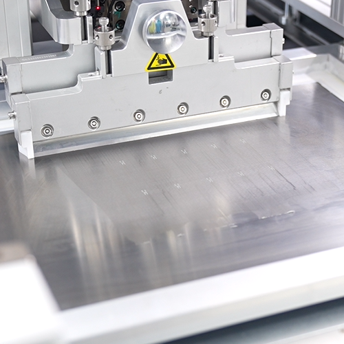
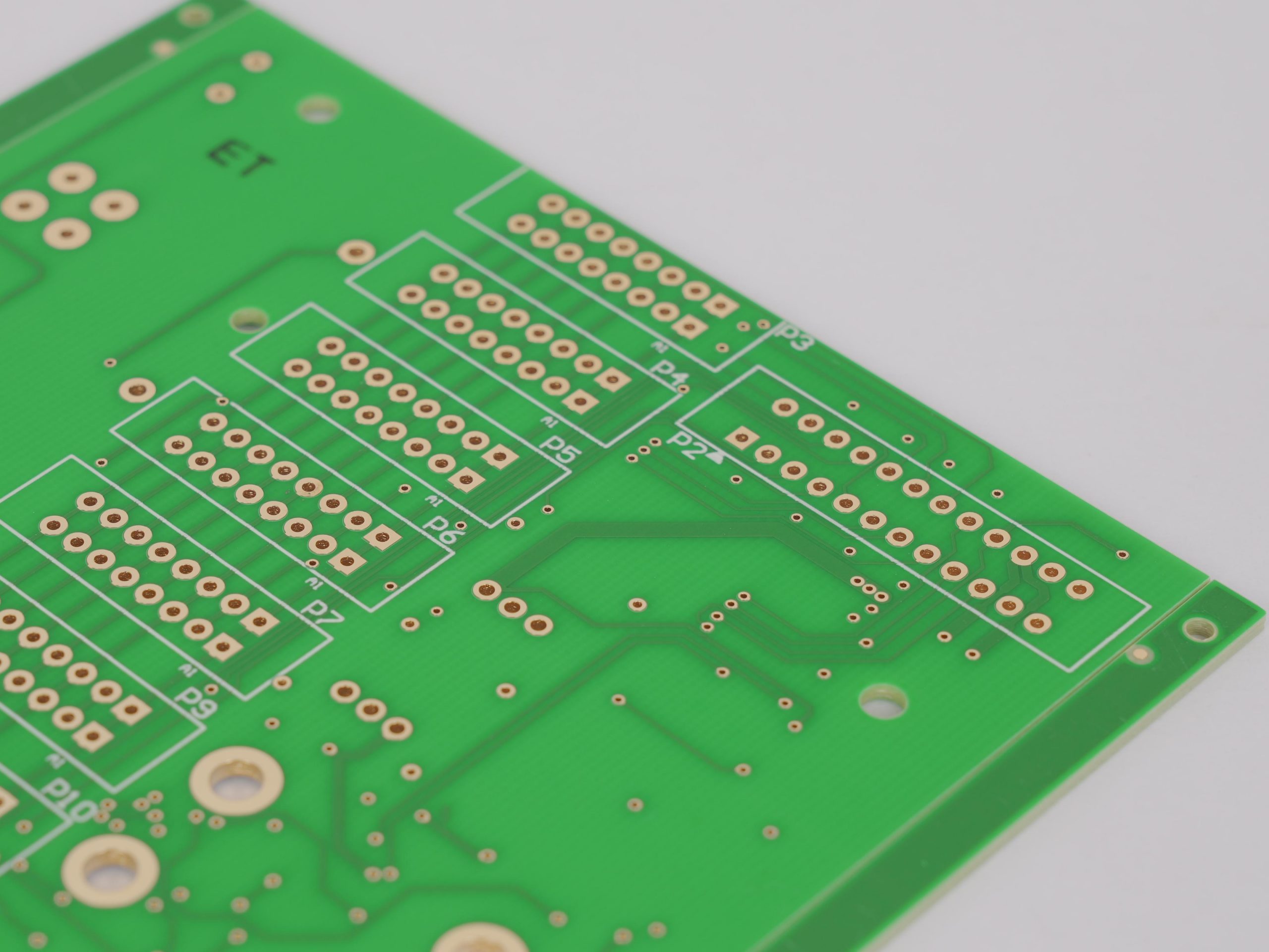
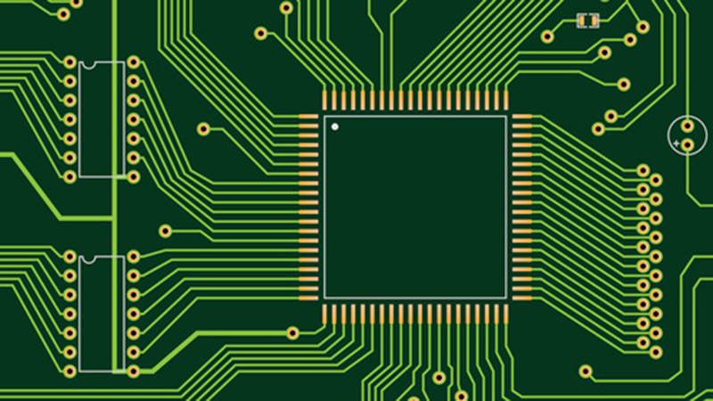
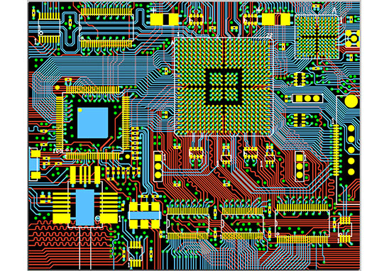
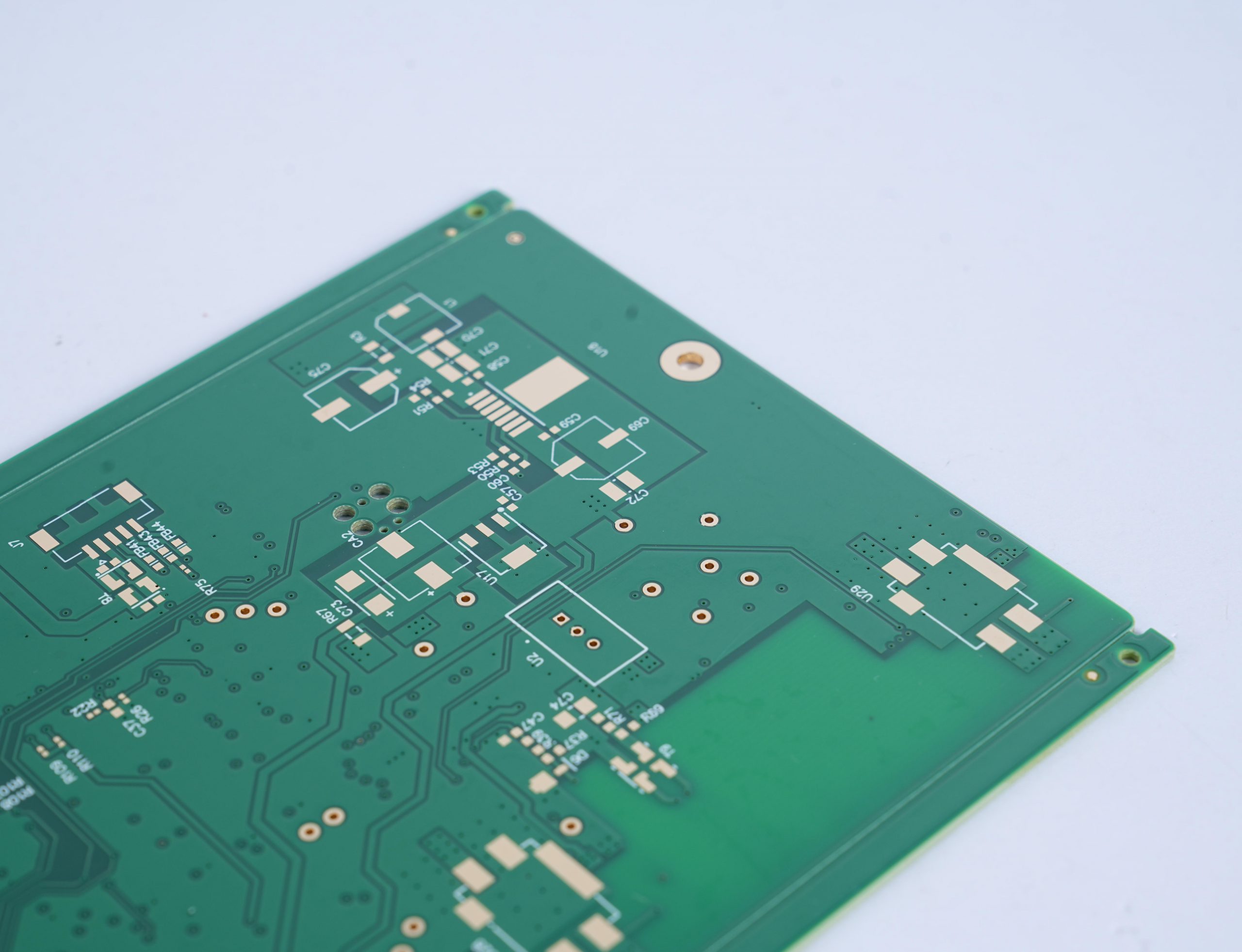
In the manufacturing process of printed circuit boards, it is very necessary to apply a proper amount of flux. The soldering pads, copper bars of components and the surface of solder paste are the places where flux should be applied, which can improve the firmness of the soldering points and the quality of printed circuit boards.

What is flux?

Flux: A chemical substance that can help and promote the soldering process in the soldering process, and at the same time has a protective effect and prevents oxidation reactions. Flux can be divided into solid, liquid and gas.

How to use solder flux?

There are mainly several aspects such as “assisting heat conduction”, “removing oxides”, “reducing the surface tension of the material to be soldered”, “removing oil stains on the surface of the material to be soldered, increasing the soldering area”, and “preventing re-oxidation”. Among these aspects, the two most critical functions are: “removing oxides” and “reducing the surface tension of the material to be soldered”.

Do you apply flux before or after soldering?

Use flux before soldering printed circuit boards. ‌

How to use solder flux?

During the soldering process of printed circuit boards, the main purpose of using flux is to improve soldering performance and help the metal avoid the formation of an oxide film that hinders solder wetting when heated, thereby promoting the formation of solder-metal alloys and avoiding the occurrence of cold soldering and false soldering.

Flux can be applied to the printed circuit board before soldering, or it can be used as part of the solder during the soldering process, such as solder paste or solder oil. When tinning the pins of components, rosin should be used as the flux, and if the printed circuit board is already coated with rosin solution, then no additional flux is required during soldering.

After using flux, make sure to wipe off the residual flux at the soldering site after soldering to avoid potential damage to electronic components and circuit boards.

In addition, the preparation work before soldering includes thoroughly cleaning the copper foil surface and then applying rosin water to protect the copper foil and help soldering. This step is performed before soldering to ensure the smooth progress of the soldering process. Therefore, the correct approach is to use flux before soldering printed circuit boards to ensure the quality and reliability of soldering.

How much flux to use when soldering?

When soldering printed circuit boards, the amount of flux used needs to be determined according to the specific soldering method and the type of flux. For wave soldering flux, when using brushing and foaming methods, the specific gravity of the flux should be controlled between 0.82-0.84 (specific gravity of liquid rosin flux stock solution).

During the soldering process, the specific gravity of the flux needs to be measured regularly. If the specific gravity is found to increase, it should be adjusted to the normal range with diluent in time, but the diluent should not be added too much to avoid affecting the soldering quality.

For the quantitative spraying method, the key is that the nozzle can control the spray volume. The nozzle should be cleaned frequently to ensure that the spray hole is not blocked. The spray pressure should be controlled at 0.2-0.3Mpa, the flux pressure should be controlled at 0.4±0.05Mpa, and the spray flow rate should be controlled at 20-35ml/min.

In addition, different types of flux formulas are also different. For example, rosin liquid can be made by mixing rosin blocks and alcohol in a ratio of 1:3. For the flux of printed circuit boards, you can directly use rosin water, and apply the prepared rosin water directly on the surface of the printed circuit board or the solder joints.

When using flux, you should also pay attention to the following points:

Put the bottle cap on immediately after use to prevent the flux from being in contact with air for a long time and causing oxidation reaction or absorbing water vapor in the air to cause the concentration to decrease.

Regularly replace the flux that has been stored for too long, because long-term storage will cause the flux composition to change and the activation performance to deteriorate, affecting the welding quality.

Clean it after welding, because the insulation performance of the flux will drop sharply at high temperature, and the residue may affect the heating components, and in severe cases may cause short circuits.

In summary, the amount of flux used in printed circuit board welding needs to be determined according to the specific welding method and flux type, and pay attention to the use and storage conditions of the flux to ensure welding quality and safety.

What happens if you use too much flux when soldering?

First, the main functions of flux include assisting heat conduction, removing oxides, reducing the surface tension of the material being soldered, removing oil stains on the surface of the material being soldered, increasing the soldering area, and preventing reoxidation.

However, excessive use of flux can lead to corrosion and electromigration. This is because improper use of flux, such as excessive use, can create more favorable conditions for potential chemical corrosion reactions.

In addition, if the flux used is not well controlled, resulting in excessive use of flux, more flux residue will be left, which creates more favorable conditions for potential chemical corrosion reactions.

Therefore, it is very important to control the amount of flux used to avoid negative effects on soldering quality and reliability.

What happens if I don’t use flux?

If flux is not used on printed circuit boards, it may lead to reduced soldering quality, increased soldering difficulty, and affect the performance and reliability of the circuit.

1. Increased soldering difficulty: Without flux, the solder may be difficult to flow to the soldering point, resulting in loose soldering, prone to cold soldering or poor soldering.

2. Reduce welding quality: Without the help of flux, the soldering point may not be smooth enough, with burrs or unevenness, which may affect the normal operation of the circuit.

3. Affect circuit performance and reliability: Flux can reduce the resistance of the soldering point and improve the conductivity of the circuit. Without flux, the resistance of the soldering point may increase, affecting the performance and stability of the circuit.

In addition, the flux can also prevent oxidation to a certain extent, protect the soldering point from the influence of the external environment, thereby improving the life of the circuit. Therefore, in the soldering process of printed circuit boards, it is very important to use the soldering flux correctly.

What is an alternative to soldering flux?

Alternatives to printed circuit board soldering flux include no-clean soldering flux, special solder resist for printed circuit boards, water-based cleaning agents and dry ice cleaning technology. ‌

1. No-clean soldering flux is a new type of soldering flux that does not contain halide activators. It does not need to be cleaned after use, which can save investment in cleaning equipment and cleaning solvents, while reducing the emission of waste gas and wastewater, and the pollution to the environment is also reduced accordingly.

2. The main function of the ‌PCB solder mask‌ is to prevent “wiring” and short circuits during wave soldering and protect the PCB permanently. In addition, it can save solder, reduce the weight of the PCB, and reduce costs.

3. As a new type of cleaning medium, the ‌water-based cleaning agent‌ achieves cleaning through the wetting, dissolution, emulsification, saponification, chelation and other effects of the surfactants, emulsifiers, penetrants, etc.

How to use solder flux?

4. The ‌dry ice cleaning technology‌ uses extremely low-temperature dry ice particles to spray onto the treated object under the action of compressed air, so that the dirt is rapidly frozen to brittleness and burst, and then vaporized to take away the dirt.

These substitutes have their own characteristics and are suitable for different application scenarios and technical requirements. When choosing, specific process requirements and cost-effectiveness must be considered.

What does rosin do when soldering?

In the process of printed circuit board soldering, rosin plays a vital role. It is mainly used as a flux to help the soldering process be smoother and more efficient. The role of rosin is reflected in the following aspects:

‌Removing oxide film‌: Rosin can remove the oxide film formed on the copper surface due to contact with air. These oxide films will prevent the tin from wetting the copper wire, thus affecting the quality of welding.

‌Preventing re-oxidation‌: Rosin can not only remove the oxide film, but also prevent the soldering surface from re-oxidizing during the welding process, which helps to maintain the stability and reliability of the welding point.

‌Isolating air‌: Under high temperature conditions of welding, rosin can isolate the air and prevent oxidation of the metal surface.

In summary, rosin plays an important role in the soldering process of printed circuit boards. Through its fluxing effect, it improves the quality and reliability of soldering and is one of the indispensable materials in electronic manufacturing‌.

Conclusion:

Flux is a key part of the soldering process. Without it, your solder will not flow smoothly through the joint and the solder will not adhere properly to the various components on the circuit board. High-quality flux is necessary to produce good solder joints.

BEST Technology is a professional PCB circuit board manufacturer with many years of experience in PCB circuit board welding. The circuit boards it produces are of extremely high quality. We have the most extensive experience to deal with all aspects of PCB welding issues.

What are the types of PCB boards?
星期一, 26 8 月, 2024

PCB (Printed Circuit Board) boards can be classified according to their constituent materials and characteristics. PCBs are classified into single-sided boards, double-sided boards, and multi-layer boards according to board applications. They are classified into flexible PCB boards (flexible boards), rigid PCB boards, rigid-flexible PCB boards (rigid-flexible boards) according to materials, etc.

PCB is an important electronic component, a support for electronic components, and a provider of electrical connections for electronic components. Since it is made using electronic printing technology, it is also called a printed circuit board. PCB is simply a thin board with integrated circuits and other electronic components.

1. Single-sided board:

On the most basic printed circuit board, parts are concentrated on one side and wires are concentrated on the other side. Because wires only appear on one side, this type of printed circuit board is called a single-sided board. Because single-sided boards have many strict restrictions on designing circuits (because there is only one side, wiring cannot cross and must go around a separate path), early circuits used this type of circuit board.

2. Double-sided board

What are the types of PCB boards?

This type of circuit board has wiring on both sides. In order to connect the wires on both sides, there must be a proper circuit connection between the two sides. This connection between the circuits is called a guide hole. A guide hole is a small hole filled or coated with metal on a printed circuit board, which can be connected to the wires on both sides. Because the area of a double-sided board is doubled that of a single-sided board, and the wiring can be interlaced (can go around to the other side), double-sided boards can be used on more complex circuits than single-sided boards.

3. Multilayer board:

In order to increase the area that can be wired, multilayer boards use more single- or double-sided wiring boards. Multilayer boards use several double-sided boards, and put an insulating layer between each layer of boards and glue them firmly. The number of layers of the circuit board represents how many independent wiring layers there are, usually an even number of layers, and includes the two outermost layers.

4. Flexible PCB board

Flexible PCB board is a printed circuit board made of a flexible substrate. Its advantage is that it can be bent, which is convenient for the assembly of electrical components. Flexible circuit board, flexible PCB, flexible circuit and multi-function printed circuit are other names for these circuit boards. These printed circuit boards are made using the same components as rigid printed circuit boards. The main difference is that the circuit board is designed to bend to the desired shape throughout the application process. These PCBs are available in single-sided, double-sided, and multi-layer configurations. This helps reduce the complexity of unit assembly.

5. Rigid PCB Board

Rigid PCB is a circuit board that cannot be twisted or folded. The base material of the board is a rigid substrate, which gives the board rigidity and strength. They are composed of multiple layers, including substrate layers, copper layers, solder mask layers, and silk screen layers, which are bonded together by adhesives and heat. While some circuit boards are single-sided, double-sided, or multi-layered, rigid PCBs can be any of these as needed. However, once made, they cannot be modified or changed.

6. Rigid-Flex Board

Rigid-Flex Board is a hybrid circuit board that combines elements of flexible and rigid circuit boards to form a foldable or continuously bendable circuit board, which is usually molded into a curved shape or curve during the manufacturing process.

What are the types of PCB boards?

The flexible portion of the circuit board is often used for interconnections between rigid circuit boards, allowing narrower wires to take up less space, thereby reducing the size of the circuit board. Using flexible PCBs for interconnections often eliminates the need for bulky and heavy connectors, making rigid-flex boards lighter. The design of rigid-flex boards is slightly more complicated because these boards are 3D constructed, allowing the board to be folded or twisted to produce the shape required for the product.

7. High-frequency PCB board

High-frequency circuits refer to the overall circuit board design, not the other types of circuit board structures we described earlier. These PCBs are designed to conduct signals over 1 GHz.

High-frequency boards mostly use FR4-grade glass-reinforced epoxy boards, polyphenylene ether (PPO) resins, and Teflon, but Teflon has a low and stable Dk value, low dielectric loss, low hygroscopicity, and is slightly more expensive.

When designing high-frequency circuits, various factors must be considered, such as Dk value, dissipative loss, and dielectric thickness. The DK value of the substrate is an important factor to remember. Substrates with a higher probability of Dk value changes usually experience impedance changes, which affects the harmonics that make up the electrical signal, resulting in poor signal integrity.

8. Copper substrate

Copper substrate is a metal substrate with high thermal conductivity, suitable for high-frequency circuits and areas with large high and low temperature changes and heat dissipation and architectural decoration industries for precision communication equipment.

The copper substrate circuit layer requires a large current carrying capacity, and a thicker copper foil should be used, with a thickness of generally 35μm~280μm. The thermal conductive insulation layer is the core technology of the copper substrate. It is composed of core thermal conductive components and high molecular polymers, with low thermal resistance (0.15), excellent viscoelastic properties, resistance to thermal aging, and the ability to withstand mechanical and thermal stress.

The copper substrate metal base is the supporting member of the copper substrate, which is required to have high thermal conductivity. It is generally a copper plate, and a copper plate can also be used (where the copper plate can provide better thermal conductivity). It is suitable for conventional mechanical processing such as drilling, punching and cutting.

9. Aluminum-based PCB board

The design of aluminum-based PCB circuits is similar to that of copper-based PCBs, but the substrate material of aluminum-based PCBs is aluminum metal, rather than the standard glass fiber used in most circuits.

What are the types of PCB boards?

The aluminum layer is reinforced with the least heat-resistant insulation material, which means less heat is transferred from the insulation material to the backing. After applying the insulation layer, another layer of copper is required.

10. High Density Interconnect (HDI) PCB

Among the many types of PCBs, HDI PCB is a circuit with multiple interconnections that takes up very little space. HDI components are mounted close to each other, minimizing PCB space while maintaining high functionality. Boards containing 120-160 pins per square inch are classified as HDI PCBs.

HDI designs integrate dense device mounting and multi-purpose wiring. With the help of microvias, buried vias, and blind vias, compact circuits can be made, minimizing drilling to copper. For the electrical requirements of high-speed signals, HDI PCBs must have high-frequency conduction capabilities, impedance control, and minimal redundant radiation.

11. Thick Copper PCB

Thick copper PCB is also called heavy copper PCB. Basically, it contains more than 2 ounces of copper in the inner and outer layers of the board. Heavy copper transmitters significantly increase the overall thickness of the board; thick copper boards are known for supporting high currents, high temperatures, and cyclical thermal cycles.

12. High TG PCB

Among various types of PCBs, high Tg PCBs are circuit boards designed to work at high temperatures. Glass transition temperature (Tg) is an essential element of any epoxy resin. It is basically the temperature point at which the polymer changes from a hard glass substrate to a soft rubber substrate. The substrates used to make high Tg circuit boards must be flame retardant, which means that they soften instead of burning at the glass transition point (Tg).

The higher the Tg value, the higher the temperature requirement during lamination. Under such conditions, the PCB will become hard and brittle, affecting the aperture size and related electrical properties. Standard boards will soften, deform and melt under such conditions, and their mechanical and electrical properties will be significantly reduced.

Standard FR-4 Tg is between 130-1400C, medium Tg is between 150-1600C, and high Tg is above 1700C. The higher the Tg value, the better the board’s heat, moisture and chemical resistance.

Conclusion:

PCB board types are updated and iterated with the rapid development of the industry, and various types of PCB boards have gradually evolved to cope with various application scenarios, adding corresponding materials according to the required performance. BEST Technology has various PCB types of manufacturing technology, which can meet your any type of PCB needs.

What is the surface mount technology?
星期五, 23 8 月, 2024

Surface mount technology (SMT) is a widely used surface assembly method in the electronic assembly industry. It mainly uses automated production equipment to directly solder surface mount components (SMD) to the pads on the surface of the printed circuit board (PCB). SMT has the advantages of high production efficiency, high space utilization, high density and miniaturization. However, it has high requirements for production equipment, processes and operating skills.

What is the surface mount technology process?

The process of surface mount technology (SMT) mainly includes the following steps:

1. Printed circuit board preparation: Before surface mounting, the printed circuit board needs to be prepared first, including cleaning the circuit board, removing the surface oxide layer, and applying solder paste.

What is the surface mount technology ?

2. Component mounting: Use appropriate equipment to accurately mount various electronic components on the printed circuit board.

3. Soldering: After the components are mounted, the solder paste is heated to melt it to form a reliable welding connection.

4. Inspection: After welding, use AOI for automatic inspection to ensure the correct mounting and welding quality of components.

5. Testing and debugging: Test and debug the mounted circuit board, and verify whether the function and performance of the circuit board meet the requirements through specific test equipment and procedures.

Each step needs to be carried out carefully to ensure that the mounted circuit board has good quality and reliability. In addition, surface mount technology is suitable for circuit board assembly, with the characteristics of compact structure and small size, and is widely used in the manufacture of electronic products.

What are the roles of surface mount?

The role of surface mount technology (SMT) is mainly reflected in improving the performance, reliability and production efficiency of electronic products, while reducing the volume and weight of products.

Surface mount technology (SMT) has the following significant effects:

Increase assembly density and reduce product volume: By using surface mount technology, the volume of electronic products can be reduced by 40%~60% and the weight can be reduced by 60%~80%.

What is the surface mount technology ?

‌Improve reliability: SMT has high reliability, low solder joint defect rate and strong vibration resistance.

Optimize high-frequency characteristics: SMT reduces electromagnetic and radio frequency interference and optimizes the high-frequency characteristics of the circuit.

Automated production: SMT is easy to automate, thereby improving production efficiency.

Enhanced compactness: Using small surface-mounted components can save a lot of space on the printed circuit board, and circuit assembly is easier to automate.

Adapt to a wide range of fields: As a new generation of electronic assembly technology, SMT has penetrated into various fields, including but not limited to computers, communication equipment, consumer electronics, etc.

In summary, surface mounting technology has significantly improved the comprehensive performance and production efficiency of modern electronic products by increasing assembly density, optimizing circuit performance, enhancing product reliability, and realizing automated production.

What is the advantage of surface mount?

The advantages of surface mounting mainly include:

High assembly density: Surface mounting technology (SMT) allows more electronic components to be installed in a limited space.

Small size and light weight of electronic products: By using SMT, smaller and lighter electronic products can be manufactured.

‌High reliability‌: SMT has a low solder joint defect rate, which improves the reliability of the product‌.

‌Easy to automate‌: SMT technology is very suitable for automated production and can greatly improve production efficiency‌.

‌Design flexibility‌: SMT allows different components to be used on the same circuit board, providing design flexibility‌.

‌EMC compliance‌: SMT technology helps meet electromagnetic compatibility (EMC) requirements and ensure the safety and performance of the equipment‌.

‌Selective soldering‌: SMT supports selective soldering, which increases the customizability of the product‌.

In addition, SMT technology is cost-effective because the packaging size of components is generally standardized and can be quickly and accurately installed using automated equipment, thereby reducing production costs‌. At the same time, SMT reduces human errors and improves product quality because the placement of components is very consistent, reducing errors or the need for rework.

What are the disadvantages of surface mount?

‌The disadvantages of surface mount technology (SMT) mainly include incompatibility with certain components, the possibility of soldering defects, and high equipment costs. ‌

‌Incompatibility with certain components‌: SMT technology is not suitable for all types of components.

‌Possibility of soldering defects‌: Although SMT technology reduces the need for drilling and shortens setup time, it is not a zero-defect soldering process. In actual applications, SMT may encounter various soldering defects.

‌Higher equipment cost‌: Although SMT technology can improve production efficiency and circuit density, it requires expensive special equipment and professional technicians.

In summary, although SMT technology has many advantages, such as reducing drilling, shortening setup time, and improving production efficiency, it also has some disadvantages, especially in terms of incompatibility with certain components, possible soldering defects, and high equipment costs.

What does SMD stand for in surface mount?

SMD stands for Surface Mounted Devices. ‌

SMD is a type of component in surface mount technology (SMT), which is characterized by small size, high power, stable performance, and easy automated assembly.

What is the surface mount technology ?

SMD packaging technology can maximize the space utilization on the circuit board, especially for the design of dense circuit boards. SMD packaging usually adopts metal oxide semiconductor (MOS) technology, and its packaging methods are diverse, including COB, QFN, LCC, BGA, etc.

In practical applications, the appearance inspection of SMD devices includes visual inspection or use of a magnifying glass to check whether the solder end or pin surface is oxidized or has contaminants, and to ensure that the nominal value, specification, model, accuracy, and external dimensions of the components are consistent with the product process requirements. To ensure the performance and reliability of the device.

The wide application of SMD technology not only improves the performance of electronic products, but also promotes the automation and efficiency improvement of the electronics manufacturing industry. It is an indispensable part of the modern electronics manufacturing industry, especially in applications that require high integration and high reliability.

What is the application of surface mount?

The application of surface mount technology is mainly reflected in improving production efficiency, reducing product volume and weight, and meeting the market demand for miniaturized, lightweight, and high-performance electronic products. This technology is mainly used to mount electronic components on printed circuit boards (PCBs) to achieve circuit connection and system integration.

Surface mount technology can replace traditional through-hole insertion technology, thereby improving product reliability and performance and reducing costs. The technology has a wide range of applications, including but not limited to consumer electronics, military cutting-edge electronics, and fire detectors, manual alarms, and various electronic modules.

In the manufacture of electronic products, surface mount technology has become a revolutionary change, dominating the development of electronic equipment and bringing about major changes in electronic products.

Conclusion:

Usually, the electronic products we use are designed by PCB plus various capacitors, resistors and other electronic components according to the designed circuit diagram, so most electrical appliances require various SMT (patch) processing technologies to process.

BEST Technology focuses on the procurement and processing of various electronic products and processing services for incoming materials, including but not limited to SMT patches, DIP plug-ins, welding, functional testing and maintenance, and assembly proofing and batch production. We can provide proofing, small batch and batch SMT mounting, and can also purchase electronic components and make PCBs.

What is a PCB assembly?
星期四, 22 8 月, 2024

PCB assembly is the process of combining a circuit board with other electronic components (such as connectors, housings, heat sinks, etc.) to embed into a final product. This process is a key step in the production of electronic equipment. Its main function is to provide a platform for electronic components to work together in a coordinated manner so that the equipment can perform its intended tasks.

What is the standard for PCB assembly?

The standards for PCB assembly mainly include PCB panel specifications, ISO standards, IPC standards, JEDEC standards, and ROHS standards. ‌

What is a PCB assembly?

‌PCB panel specifications‌ involve the width, shape, frame design, center distance between small boards, setting of positioning holes, arrangement of reference symbols, and positioning of large components of the panel. The panel frame should adopt a closed-loop design to ensure that the panel is fixed on the fixture without deformation.

‌ISO standards‌ emphasize key factors such as fit tolerance, surface roughness, contact area, and tightening force in PCB tight-fit installation to ensure the accuracy and stability of installation‌.

‌IPC standards‌ include IPC-7711 and IPC-A-600E, the former provides basic recommendations and guidelines for the design and manufacture of printed boards, and the latter provides acceptable conditions and practice guidelines for printed boards.

‌JEDEC standards‌ provide specifications for circuit board materials, dimensions, interfaces, etc., including material selection, dimension design, interface specifications, test methods and quality assurance.

‌ROHS standard‌ is a directive on the restriction of the use of hazardous substances, aimed at reducing the impact on the environment and human health. It stipulates the use restrictions of hazardous substances such as lead, mercury, cadmium, hexavalent chromium, polybrominated biphenyls and polybrominated diphenyl ethers.

Compliance with these standards ensures the quality, safety and environmental friendliness of PCB products, and also provides clear guidance and specifications for the design, manufacture and assembly of PCBs.

Why is PCB assembly so expensive?

The high cost of PCB assembly is mainly due to the combined influence of multiple factors. ‌

First, the production cost of PCB boards is affected by materials, design and manufacturing complexity, precision and quality, and supply chain and regional differences. PCB boards are mainly made of materials such as copper, fiberglass and epoxy resin, and the cost of these materials directly affects the price of PCB boards.

The complexity of the design and manufacturing process, including pre-processing, image transfer, electroplating, etching, inspection and trimming, and post-processing, requires precise tools and professional skills, which will also be reflected in the cost. High-precision PCB boards require higher manufacturing costs because they require more precise tools and more stringent manufacturing processes.

Details in the PCB assembly process, layer selection, and the application of HDI technology will all have an impact on the cost. Every small change may cause the cost to plummet, so if you want to save money without losing performance, you need to consider these factors comprehensively.

In addition, the welding process is also a costly link. Soldering is a key step in fixing electronic components to PCBs. This process requires heating each joint separately for welding, which is a slow and laborious process.

Finally, the price of PCBs is also affected by factors such as materials, surface processing, design standards, copper foil thickness, quality acceptance standards, and mold fees and test frames. For example, different materials, surface processing, and copper foil thickness will lead to price differences.

In summary, the high cost of PCB assembly is mainly due to the combined effect of multiple factors such as material cost, manufacturing complexity, precision and quality requirements, production needs, and specific design and quality requirements.

What does PCB stand for?

PCB stands for Printed Circuit Board. ‌

What is a PCB assembly?

Printed circuit board (PCB), also known as printed circuit board, is an indispensable component in electronic engineering. It is the support of electronic components and also the carrier of electrical connection of electronic components.

Printed circuit boards are widely used in various electronic devices. Printed circuit boards can be divided into single-sided boards, double-sided boards, multi-layer boards, etc. according to the number of layers of circuit boards. Among them, multi-layer boards refer to printed boards with more than two layers. It consists of connecting wires on several layers of insulating substrates and pads for assembling and welding electronic components. It has the function of conducting each layer of circuits and insulating each other.

The wide application of printed circuit boards makes it possible to miniaturize and visualize the circuits of electronic devices, which plays an important role in the mass production of fixed circuits and optimizing the layout of electrical appliances. This type of circuit board uses polyimide or polyester film as the substrate, and has the characteristics of high wiring density, light weight, thin thickness and good bendability.

What is the difference between PCB and PCBA?

The main difference between PCB and PCBA lies in their definition, function, application and manufacturing process. ‌

Definition:

PCB (printed circuit board) is a basic electronic component made by electronic printing, mainly used as a support for electronic components, and does not contain any active or passive components.

PCBA (printed circuit board assembly) is a circuit board assembly with specific functions formed by soldering electronic components to PCB through processes such as SMT (surface mount technology) or THT (through-hole mounting technology). PCBA contains PCB and all necessary electronic components, which work together to realize the preset functions of the circuit board.

What is a PCB assembly?

‌Function and application‌:

The main function of PCB is to support and connect electronic components, while PCBA integrates electronic components into a complete circuit system, which can be used in the manufacture of various electronic products.

PCBA is the core part of electronic products and directly determines the performance and function of the product.

‌Manufacturing process‌:

The manufacturing process of PCB includes circuit design, PCB board design, PCB template production, copper foil etching, drilling, tin spraying and board making.

The production of PCBA requires component mounting, welding, testing and other processes.

In summary, the main difference between PCB and PCBA lies in their definition, function, application and manufacturing process. PCB is a basic electronic component, mainly used to support and connect electronic components, while PCBA is a finished product formed by welding electronic components to PCB. It has specific circuit functions and is an indispensable part of electronic products.

What is the difference between PCB manufacturing and assembly?

The main difference between PCB manufacturing and assembly is that they involve different processes and focuses. ‌

‌PCB manufacturing‌ mainly involves the process of converting raw materials into printed circuit boards through a series of process flows, including design, layout, etching, lamination, drilling, welding and other steps, and finally forming a complete and usable printed circuit board.

‌PCB assembly‌ is the process of soldering electronic components to the printed circuit board according to the design requirements after the PCB is manufactured. The focus of assembly is to ensure that all components are in the correct position and direction, the pins of each component are fully soldered to the designated pads, and there is no excess solder or other excess materials to ensure the normal operation and reliability of the circuit board.

In short, ‌manufacturing‌ covers the entire production process from raw materials to finished products, including design, production and testing, while ‌assembly‌ is a link in the manufacturing process that focuses on accurately mounting electronic components on printed circuit boards to ensure the final function and performance of the product.

Conclusion:

PCB assembly is an important part of manufacturing and affects the quality of the final product. Therefore, choosing the right manufacturer becomes particularly important. BEST Technology is committed to becoming the world’s most trusted one-stop electronic circuit solution provider, while focusing on PCBA prototyping and small batch production. Choosing us will get the best quality products.

How to design a PCB board?
星期四, 22 8 月, 2024

PCB design is an indispensable part of modern electronic product development. An efficient and reliable PCB design can ensure the normal operation of the circuit and meet the performance and manufacturability requirements of the product.

PCB design (Printed Circuit Board Design) refers to the design of circuit boards using electronic design automation software (EDA), designing the layout and circuit connections of printed circuit boards (PCBs). Circuit boards are an important part of electronic products. They can connect electronic components together and transmit signals through wires.

Is PCB design hard to learn?

PCB design is not difficult to learn. The key lies in mastering the relevant basic knowledge and practical experience.

How to design a PCB board?

PCB design mainly involves electronic circuit knowledge and software operation skills. For people with electronic circuit foundation, it is relatively easy to learn the use of PCB design software. It is important that learners should use their spare time to learn and practice at the same time. They can assist in learning by watching video tutorials. These resources can help understand the basic concepts and skills of circuit design and software operation.

In addition, the difficulty of PCB design lies mainly in the design of wiring rules, which is the most complex and critical part of PCB design. Beginners should pay attention to the design of conventional constraint rules, such as the size of vias, line width and line spacing, etc., which need to be mastered through practical operation and practice. Just reading materials is not enough. Practical operation and practice are the key to improving PCB design capabilities.

In general, although PCB design involves certain technical difficulties, it can be gradually mastered through systematic learning and practice.

What should I learn before PCB design?

Before PCB design, you need to learn the following key knowledge and skills:

1. Basic knowledge reserve: First of all, you need to understand various electronic components, such as resistors, capacitors, inductors, diodes, triodes, integrated circuits, etc. You also need to be familiar with common circuit topologies, such as amplifier circuits, filter circuits, oscillation circuits, and their functions and representation methods in circuits.

How to design a PCB board?

2. PCB design software: Be proficient in at least one PCB design software for schematic design, component layout, wiring, and generation of PCB production files, such as Altium Designer, EAGLE, PADS, OrCAD, etc.

3. Circuit board manufacturing process: Understand the manufacturing process of PCB circuit boards, including substrate material selection, circuit pattern transfer, etching, drilling, welding, assembly, etc.

4. Component packaging: Familiar with the packaging types and sizes of various components, such as DIP, SOP, QFP, BGA, etc., as well as their characteristics and usage scenarios.

5. Basic terms and concepts: Master some basic PCB terms, such as microstrip, stripline, differential line, via, solder mask, silk screen, structural diagram, etc.

6. Circuit function and signal flow: Understand the function and signal flow of the circuit, and be able to distinguish between digital circuits and analog circuits, as well as places with large and small currents.

By mastering the above knowledge and skills, you can better design and layout circuits, improve the performance and reliability of circuit boards,

Which software is used for PCB design?

1. Altium Designer is a powerful PCB design software that provides a wealth of tools and libraries to quickly create complex circuit board designs. This software has an intuitive interface and powerful simulation functions to help designers quickly verify the correctness of the design. It also supports multiple design file formats, which is convenient for collaboration with other design tools.

2. Cadence Allegro is a comprehensive circuit board design software with powerful layout and routing tools, as well as multiple simulation and verification tools to ensure the correctness of the design. It also supports multiple design file formats for team collaboration.

3. Mentor Graphics DesignX is also a powerful PCB design software that provides a variety of tools and libraries to help designers quickly create complex circuit board designs. It also has an intuitive interface and powerful simulation functions, and supports multiple design file formats.

4. PADS is a professional circuit board design software with powerful layout, routing, simulation and verification functions, which can quickly complete complex PCB design work. It also supports multiple design file formats, which is convenient for collaboration with other design tools.

These software are all commonly used PCB design tools with powerful layout, routing, simulation and verification functions, which can help designers quickly complete complex PCB design work.

What is the basic rule of PCB design?

The basic rules of PCB design involve many aspects, including layout, routing, power and ground design, signal integrity, etc.

How to design a PCB board?

1. Layout design:

Follow the design principle of placing in a straight line along the signal flow direction to avoid the signal from circling back and forth to reduce the impact of direct signal coupling.

The filtering, protection and isolation devices of the interface circuit should be placed close to the interface to achieve effective protection, filtering and isolation effects.

For high-speed signals or high-current signals, multi-layer board design should be considered to control the signal loop area.

2. Wiring rules:

Control the length of the trace, especially for important signal lines, such as clock signals, the trace length should be shortened as much as possible to reduce unnecessary interference.

Avoid forming self-loop traces to reduce radiation interference.

Follow the principle of minimum ground loop, design the signal line and its loop to form the smallest possible loop area to reduce external radiation and external interference.

3. Power and ground design:

The power plane should be retracted a certain distance relative to its return ground plane to effectively suppress edge radiation problems.

Avoid overlapping of different power layers in space to reduce interference between different power supplies.

4. Drawing:

When drawing the board frame, a specific line width should be used to ensure that the error between the board frame size and the assembly size is within the allowable range.

Set a reasonable origin to ensure that the coordinates of the SMT original are within the first quadrant.

Set a prohibited area, especially prohibiting routing and placing components within a certain range around the mounting hole.

Following these basic rules can ensure the effectiveness and reliability of PCB design, while improving product performance and user experience.

How long does it take to design a PCB board?

It takes about 1-2 days to design a PCB board, and the specific time depends on multiple factors, including the number of layers of the PCB, design complexity, etc.

‌Number of layers and complexity‌: The more layers the PCB has, the more complicated the design process is, and more time and delicate work are required to ensure the correctness and performance of the circuit.

‌Design stage‌: PCB design includes multiple steps such as design layout, schematic drawing, and PCB design conversion.

The time to design a PCB board is a comprehensive estimate involving multiple stages and factors.

What is the proper PCB layout?

Proper PCB layout involves many aspects, including structural requirements, heat dissipation considerations, component spacing, routing rules, etc. ‌

‌Structural requirements‌: First, the PCB layout must meet the structural requirements, including the location arrangement of structural components such as power sockets and DVI interfaces.

‌Heat dissipation considerations‌: The distribution of heat sinks should be even to ensure good ventilation of the air path. Avoid heat sinks blocking the air path to avoid affecting the heat dissipation effect‌.

‌Component spacing‌: Capacitors, ICs, etc. should be kept away from thermal components to avoid being affected by heat.

‌Routing rules‌: The design of the current loop should consider the convenience of threading, and the lead hole spacing should not be too far or too close. The layout of input/output and AC/socket should meet the consistency of the length of the two lines, leaving a certain space margin, and pay attention to the position of the plug wire buckle and the convenience of plugging and unplugging‌.

‌Special component layout‌: For high-frequency components and components with high potential difference, the distance between them should be increased to avoid electrical interference and damage.

Wiring design parameters‌: including the line width of the copper trace, the minimum gap between the copper foil traces, the minimum distance between the copper foil traces and the edge of the PCB board, etc. ‌ .

In summary, the correct PCB layout is a process that comprehensively considers the structure, heat dissipation, component spacing, routing rules and wiring design parameters, aiming to optimize the performance and reliability of the circuit board.

Conclusion:

Designing a PCB board is a complex and meticulous process involving multiple steps and considerations. Systematically complete the design process of a PCB board. Each step requires careful operation and multiple checks to ensure the quality and reliability of the final product. ‌ BEST Technology’s PCB designers have many years of design experience and are far ahead in the industry design. We can meet any PCB design you need.

What are the factors that affect the price of PCB boards?
星期二, 20 8 月, 2024

There are many factors that affect pcb board price. The diversity of PCB processing prices has its inherent inevitable factors, which are closely related to materials, processes and other aspects. As an important part of electronic components, PCB boards play a very important role in the electronics industry. One of the important problems is that prices fluctuate greatly, which brings great uncertainty to the production and operation of enterprises.

How much do pcb board price?

The price of PCB is determined by many factors, including board cost, processing cost, quality inspection cost, etc. ‌

‌Board cost‌ is the main component of PCB cost, accounting for about half of the total cost. The cost of boards depends on factors such as material, thickness, size and quality. For example, the prices of different types of plates such as FR4, CEM-1, and aluminum substrates vary significantly. The cost of panels will be affected by multiple factors such as market supply and demand, raw material price fluctuations, and the complexity of the production process.

What are the factors that affect pcb board price?

‌Processing costs‌ include cutting, drilling, electroplating, lamination and other links. The equipment and process requirements of each link will affect the final cost. The depreciation costs of high-end equipment, workers’ operational proficiency and the degree of optimization of the production process are all key factors that affect processing costs.

‌Quality inspection cost‌ is also an important part of PCB cost. Strict quality testing is required during the production process, including environmental adaptability testing, electrical performance testing, etc. The number and stringency of these testing items will also affect production costs.

In addition, the cost of PCB also includes indirect costs, such as equipment depreciation expenses, labor costs, management expenses, R&D expenses, etc. Batch size and yield control are also important factors that affect cost. Large-volume production usually reduces unit costs, and high yield means lower costs. Therefore, the specific cost of PCB needs to be comprehensively evaluated based on factors such as specific board type, processing requirements, testing standards, and production batches.

Why is PCB so expensive?

‌The price of PCB is high mainly because its production involves multiple cost factors and complex processes. ‌

The production cost of PCB is affected by the cost of materials.

PCB boards are mainly made of materials such as copper, fiberglass, and epoxy resin. The cost of these materials directly affects the final price of the PCB board. In addition, the complexity of PCB design and manufacturing is also an important factor affecting the price. The design and manufacturing process requires precise tools and specialized skills. The more complex the design, the higher the fees paid to the designer. The complexity of the manufacturing process will also lead to increased costs.

Accuracy and quality are also key factors in determining pcb board price.

High-precision PCBs require higher manufacturing costs because they require more precise tools and more rigorous manufacturing processes. High-quality PCBs usually need to go through more quality control steps, which also increases costs.

Supply chain and regional differences are also factors that affect pcb board price.

Changes in the global supply chain and differences in production costs in different regions will be reflected in pcb board price.

In terms of production process.

PCB production includes multiple stages, such as pre-processing, image transfer, electroplating, etching, inspection and trimming, and post-processing. Each stage requires specific technology and equipment, which also increases production costs.

In addition, the price of PCB is also affected by a variety of other factors, including surface treatment technology, copper foil thickness, customer’s quality acceptance standards, mold fees and test rack fees, payment methods and order volume/delivery time, etc. For example, different surface treatment processes (such as OSP, leaded tin spraying, lead-free tin spraying, etc.) and copper foil thickness will lead to price differences; the higher the customer’s quality acceptance standards, the higher the price; mass production may require Molds and test racks, which also add cost.

To sum up, the high price of PCB is mainly due to the fact that its production involves a variety of materials, complex processes, high precision and quality requirements, and a variety of factors that affect cost.

How much gold is in a PCB board?

‌PCB boards contain a certain amount of gold, but the exact amount varies depending on the type and application of the PCB board.

What are the factors that affect pcb board price?

PCB board (printed circuit board) is an indispensable component of most electronic products and is used to interconnect circuits. With the development of technology, some special electronic copper-clad laminates can even be used directly to manufacture electronic components.

In the manufacturing process of PCB boards, gold is often used as a material for surface treatment, especially in some high-end or special application PCB boards. For example, components such as motherboards, CPUs, random access memory chips (RAM), internal modems, PCI boards, Ethernet ports, etc. often contain gold on their connection pins and surface layers. The use of this gold not only increases the value of the product, but also improves its performance and reliability‌.

As for the specific gold content, although there is no fixed ratio, data shows that 1 ton of circuit boards contains at least 80 grams of gold, and chip packaging also contains gold and other precious metals such as silver. This shows that recycling precious metals such as gold from electronic waste has considerable economic value‌. In addition, the application of gold in PCB boards is usually achieved by electroplating. Sometimes a layer of nickel is added between gold and copper as a barrier layer to prevent electron migration and diffusion reactions between them.

To sum up, although the gold content in PCB boards is not high, its existence is crucial to improving the performance and reliability of electronic products, and it also has certain economic value in electronic waste recycling.

How much does it cost to replace a PCB board?

Cost estimation method in PCB processing factory The cost of PCB is composed of many factors. Most of the cost comes from the number of layers, material, drilling volume, surface treatment process, etc. of the board. Generally speaking, the cost of the board is about 1% of the total cost. About half.

According to speculation, the processing cost of PCB with more than 6 layers of material per square centimeter can be estimated as follows:

(1) For every two additional layers of the line, the cost increases by 0. 05 yuan, that is, 0. 05 yuan/cm2;

(2) Screen printing layer and solder mask layer, film cost, 300 yuan;

(3) The circuit layer film fee is 100 yuan per layer.

Actual costs should be inquired from the manufacturer.

Design requirements (1) Among the PCB processing costs, the board cost accounts for about half. Therefore, the smaller and thinner the board size, the higher the utilization rate, and the lower the cost.

(2) In terms of surface treatment, based on spray tin spraying, the surface treatment cost OSP is about 20% lower, ENIG is about 20% higher, and Im-Sn and Im-Ag are basically the same as spray tin spraying.

(3) The number of laminations has a greater impact on the cost. Each additional time will increase the total cost by about 3%.

(4) Special processes, such as buried copper, are relatively expensive and require separate communication with the manufacturer.

(5) The cost of line width/line spacing less than or equal to 3mil/3mil is about 6% higher than the cost of greater than 3mil/3mil.

(6) Adding one stage to the HDI board will increase the cost by about 18%. Therefore, the use of HDI needs to be carefully considered.

Are old PCBs worth anything?

Old PCBs not only have economic value, but also have important significance and value in environmental protection, art, etc.

pcb board price?

There are a lot of gold elements on old PCBs, because circuit interfaces are often plated with gold to increase contact performance and prevent corrosion. In addition, waste printed circuit boards also contain a variety of valuable metals. The main direction of recycling waste circuit boards is the recycling of metals.

These circuit boards contain a large amount of precious metals and rare materials. According to data, the metal contains about 20% copper, 8% iron, 2% nickel, 4% tin, 2% zinc and other common metals, and about 0.1 % gold, 0.2% silver, 0.005% palladium and other precious metals, and also contains many toxic and harmful heavy metals, such as lead, hexavalent chromium, mercury, cadmium, etc. With the right recycling techniques and processes, these valuable materials can be extracted and used to produce new electronic products.

This can not only save resources and reduce damage to the natural environment, but also effectively reduce production costs. Therefore, discarded PCB circuit boards should not be simply regarded as garbage, but should be regarded as a valuable resource.

With a combination of technology and creativity, electronics enthusiasts and artists have discovered a variety of ways to transform discarded circuit boards into unique pieces of art, home décor, or functional items. Through careful disassembly and reassembly, these discarded circuit boards are given a new life.

How can I make PCB cheaper?

1. ‌Optimized design‌: Correct component placement and layout design can significantly reduce PCB costs and improve circuit performance‌.

2. ‌Choose the right material‌: Choose the right PCB material according to the application scenario.

3. Optimize line spacing: By optimizing line width and line spacing, you can avoid additional adding.

4. Optimize the process‌: Use more efficient manufacturing processes such as the V-cut process to reduce material waste and improve sheet utilization.

5. ‌Mass production and panelization‌: Carry out mass production according to demand, enjoy batch discounts and discounts, and reduce unit prices‌.

6. ‌Technical improvement‌: Introduce advanced equipment and processes to improve production efficiency and reduce error rates, thereby reducing production costs‌.

Through the comprehensive application of the above strategies, the cost of PCB can be effectively reduced while ensuring product quality and production efficiency.

Conclusion:

Understanding the factors that affect pcb board price during the production and processing stages can help you make cost-effective decisions to ensure the quality of your products while saving money. BEST Technology has extensive design and production experience in PCB manufacturing and can effectively help you solve pcb board price issues.

Comprehensive understanding of flex board
星期二, 20 8 月, 2024

flex board are the only solution to meet the requirements of miniaturization and mobility of electronic products. They can be bent, wound, and folded freely, and can withstand millions of dynamic bending without damaging the wires. They can be arranged according to the requirements of spatial layout, and can be freely moved and stretched in three-dimensional space to achieve the integration of component assembly and wire connection. Flexible circuit boards can greatly reduce the volume and weight of electronic products, and are suitable for the development of electronic products towards high density, miniaturization, and high reliability.

What is a flex board?

Flexible board is a printed circuit board made of flexible insulating substrate, also known as flexible printed circuit board (FPC). This circuit board has many advantages that rigid printed circuit boards do not have, such as it can be bent, wound, folded freely, and can withstand millions of dynamic bending without damaging the wires. Flexible circuit boards provide excellent electrical performance, meet the design needs of smaller and higher density installations, help reduce assembly processes and enhance reliability. It is the only solution to meet the requirements of miniaturization and mobility of electronic products, which can greatly reduce the volume and weight of electronic products and adapt to the needs of electronic products developing towards high density, miniaturization, and high reliability.

Comprehensive understanding of flex board

The main feature of the flexible board is that its substrate is usually polyimide or polyester film. This material has good elasticity and a certain degree of softness, which allows the flexible board to move and stretch arbitrarily in three-dimensional space, realizing the integration of component assembly and wire connection. In addition, the flexible board also has the characteristics of high wiring density, light weight, thin thickness and good bendability, making it the preferred choice in many application scenarios.

The application of flexible boards is very wide. For example, in new energy vehicles, the FPC solution has become the main choice for most new models. FPC is integrated with CCS (integrated busbar system) and is connected with copper and aluminum busbars and plastic structural parts to form electrical connection and signal detection structural components.

What is a Flexboard made of?

Flexible boards are made of polyimide or polyester film. ‌

Flexible circuit board (FPC) is a printed circuit board with high reliability and excellent flexibility. Its substrate is mainly polyimide or polyester film. This material selection gives FPC a variety of superior properties, including high wiring density, light weight, thinness and good bendability. These characteristics of FPC enable it to meet the needs of electronic products to develop in the direction of high density, miniaturization and high reliability.

Specifically, the substrate characteristics of FPC include:

‌Polyimide‌: This is a high-performance polymer with excellent mechanical properties, electrical properties and thermal stability. It is often used to manufacture flexible circuit boards because it can provide excellent flexibility and durability.

‌Polyester film‌: As a lightweight material, the application of polyester film in FPC provides good insulation performance and certain mechanical strength while maintaining overall lightness and thinness.

The choice of these two materials together ensures that the application of FPC in electronic devices can provide excellent electrical performance, meet the design needs of smaller and higher density installation, and help reduce assembly processes and enhance reliability.

Which flex material is best?

The best material for flexible PCB boards is polyimide. Polyimide has extremely strong toughness and scalability, and can meet the requirements of bending, folding, twisting, etc. in various shapes, which makes polyimide an ideal material for flexible PCB boards. In addition, polyimide also has good impedance control and signal integrity, ensuring the high reliability and stability of flexible PCB boards. Therefore, for application scenarios that require high flexibility and reliability, polyimide is the preferred flexible PCB material.

How many types of flex board are there?

There are four main types of flexible boards:

Single-sided flexible board: This is the most basic type of flexible circuit board, in which only one side has conductive lines. It is usually used for low-density and low-complexity applications, such as printer inkjet cartridges and computer memory.

Comprehensive understanding of flex board

Double-sided flexible board: This type of circuit board has conductive lines on both sides, and the electrical connection between the two sides is achieved through metallized vias.

Multi-layer flexible board: Multi-layer FPC consists of several layers of conductive lines and insulating materials, and the electrical connection between the layers is achieved through blind holes, buried holes or through holes.

Rigid-flex combination flexible board: This type combines a rigid substrate and a flexible substrate, and a conductive connection is formed through metallized holes. Rigid-flexible combined flexible boards meet the needs of electronic products to develop in the direction of miniaturization, high frequency, high speed and multi-function.

These different types of flexible boards are widely used in consumer electronics, automotive electronics, medical equipment, aerospace and defense, etc. according to their specific application requirements and design complexity.

What is the thickness of a flex board?

The thickness of a flexible circuit board (FPC) usually ranges from 0.1mm to 0.2mm. ‌This thickness range applies to single-layer and double-layer flexible circuit boards. For multi-layer flexible circuit boards, due to their complex manufacturing process and high cost, the thickness is uncertain.

The thickness range of the reinforcement board is wider, from 0.05mm to 0.1mm for thin reinforcement boards to 0.2mm to 0.5mm for thick reinforcement boards, and even ultra-thick reinforcement boards with a thickness of more than 0.5mm. The thickness selection of these reinforcement boards depends on the design requirements, the use environment and the required mechanical strength.

The material of flexible circuit boards usually includes polyimide (PI), and its thickness generally ranges from 12.5um (0.5mil) to 125um (5mil), and common specifications include 25um (1mil) and 12.5um (0.5mil). This information shows that the thickness of flexible circuit boards can be adjusted according to specific application requirements and designs, from thin to thick reinforcement boards, to meet different mechanical strength and stability requirements.

In general, the thickness selection of flexible circuit boards is very flexible and can be customized according to specific application scenarios and design requirements. Whether it is a single-layer, double-layer or multi-layer flexible circuit board, its thickness can be adjusted as needed to ensure the best electrical performance and mechanical strength. ‌

Why are Flex PCBs so expensive?

The high price of flexible PCBs (flexible circuit boards) is mainly caused by factors such as its material cost, the complexity of the manufacturing process, and technical requirements. ‌

‌Material cost‌: The main substrates of flexible PCBs include polyimide (PI) and polyester (PET). Polyimide has excellent heat resistance and electrical properties, but the price is higher; polyester has lower cost, but the performance is slightly inferior. In addition, the conductive layer is usually composed of copper foil, and factors such as foil thickness, copper purity and quality will also affect the cost.

‌Manufacturing process‌: The manufacturing process of flexible PCB is complex, including multiple links such as exposure, development, etching, lamination and testing. The process accuracy and equipment level of each link will affect the production cost‌.

‌Technical requirements‌: The design complexity, special requirements and gold finger surface treatment methods of flexible PCB in the production process will affect the cost. Complex circuit design requires more design time and process control, while special requirements such as high temperature resistance, moisture resistance, and bending resistance require different processes and difficulties, which increase the manufacturing cost‌.

‌Size and circuit structure‌: The cost of flexible PCB is also affected by size and circuit structure. Larger size and complex circuit structure will increase manufacturing cost.

In summary, the high cost of flexible PCB is mainly due to the combined effect of factors such as high material cost, complex manufacturing process, high technical requirements, and complexity of size and circuit structure.

Conclusion:

Compared with traditional hard boards, flexible boards have higher flexibility and bendability, adapt to various complex shapes and spatial layouts, and make circuit board design more flexible and diverse. With the advantages of small size and light weight, it greatly reduces the size and weight of the device, making it more convenient to carry electronic equipment. For the design and manufacture of various flexible circuit boards, you can contact BEST Technology, and we will provide you with comprehensive and best quality services.

What is a heavy copper PCB?
星期一, 19 8 月, 2024

With the development of society, the demand for heavy copper PCBs in different industries has become increasingly greater. At present, heavy copper PCBs have been widely used in various electronic industries. Generally speaking, heavy copper technology can realize complex switches in a limited space, combine circuits with high current levels, and is conducive to heat dissipation. Multilayer and double-sided are the most common designs we know. More importantly, heavy copper PCB technology makes it possible to combine good layout structures on the outer layer and Heavy copper layers on the inner layer.

What is a heavy copper PCB?

Heavy copper PCB is a special printed circuit board (PCB) characterized by a very high concentration of copper, usually up to 200 ounces per square foot, and the copper content of the inner and outer layers of the circuit board is above 3 ounces (oz), which enables heavy copper PCBs to conduct extremely high currents, achieve good heat distribution, and realize complex circuit layouts in a limited space.

What is a heavy copper PCB?

In the design and manufacturing process of heavy copper PCBs, thermal stress handling is an important consideration. Engineers need to eliminate thermal stress as much as possible to maintain the circuit while minimizing the power budget, while taking into account environmentally friendly design.

With the development of PCB manufacturing process, modern manufacturing technology such as the use of aluminum PCB can better handle thermal stress problems.

The heat dissipation capacity of Heavy copper PCB is better than the traditional solution of using external heat sink, because it prints the heat sink directly on the circuit board during the manufacturing process, and achieves rapid heat transfer through conductive through-holes, thereby improving heat dissipation performance.

In general, Heavy copper PCB is a high-performance electronic component carrier, which provides an ideal solution for applications requiring high power and high reliability through its high copper content and optimized thermal management characteristics.

What is the difference between PCB and Heavy copper PCB?

Copper board and Heavy copper board look similar in name, and people tend to think that they are the same PCB, but in fact they refer to different things.

1. PCB:

PCB refers to a copper-based PCB. The use of copper as a substrate is to better dissipate heat and extend the life of components on the PCB. The copper substrate is to allow heat to be quickly transferred from the PCB to the outside, such as a heat sink or a metal casing. Because the thermal conductivity of copper is several times that of aluminum or other metals, up to 401W/MK.

What is a heavy copper PCB?

2. Heavy copper PCB:

Heavy copper PCB refers to PCB with copper thickness exceeding 3OZ. The substrate can be aluminum or FR4. Heavy copper is to enable PCB to carry large current. Please note that Heavy copper here does not refer to the thickness of PCB, but the thickness of copper foil on PCB. Both aluminum PCB and FR4 PCB can thicken the copper foil.

What is the maximum copper thickness on Heavy copper PCB?

‌The maximum thickness of copper on Heavy copper PCB can reach 20oz. ‌

In circuit board design and manufacturing, copper thickness is an important parameter, which directly affects the electrical performance, heat dissipation capacity and mechanical strength of the circuit board. For applications that need to carry large currents, it is necessary to choose a thicker copper layer.

The copper layer thickness of Heavy copper ultra-thick PCB is generally between 2oz and 20oz. This range of copper layer thickness can ensure the stability and reliability of the circuit board while providing good heat dissipation performance.

 In practical applications, according to international standards, the copper thickness of PCB boards can be divided into standard copper thickness and non-standard copper thickness. Standard copper thickness includes 1oz (35um) and 2oz (70um), while non-standard copper thickness covers 0.5oz (17um), 3oz (105um) and 4oz (140um). For some special applications, such as high-power LED lights, electronic high-frequency circuits, etc., a higher copper thickness may be required. At this time, non-standard copper thickness will be selected, up to 20oz.

During the manufacturing process, a Heavy copper foil is first adhered to the substrate, and then the circuit pattern is transferred to the copper foil through a photolithography process. Then chemical etching is performed to remove excess copper, and finally the thickness of the copper layer is further increased through an electroplating process to ensure that the Heavy copper PCB can meet the requirements of high current and high power applications.

Finally, surface treatment is performed to protect the copper circuit from oxidation and corrosion. Common surface treatment methods include hot air leveling (HASL), lead-free tin spraying, nickel gold (ENIG), etc. During the entire manufacturing process, process parameters must also be strictly monitored to ensure the uniformity and thickness consistency of the copper layer.

What are the advantages of Heavy copper PCBs?

1. Heavy copper PCBs have better current conductivity and can withstand excessive current loads. Because thicker copper wires have higher current carrying capacity, their current carrying capacity can be increased by increasing the copper wire width.

2. Heavy copper inner layers are ideal power distribution layers in multi-layer PCBs, which minimize ground bounce and power supply noise

3. Improve thermal performance and increase heat dissipation. Can withstand repeated thermal cycles during manufacturing and assembly.

4. Provide high mechanical strength in connector locations and plated through holes.

5. Due to the presence of copper layers, the size of the circuit board is reduced.

What are the disadvantages of Heavy copper PCBs?

1. Heavy copper PCBs are more expensive to manufacture than standard PCBs because more specialized equipment and richer expertise are required.

2. Heavy copper PCBs are more difficult to process because the PCBs may be heavier and bulkier than other PCBs.

What are the properties of Heavy copper PCBs?

High mechanical strength: After Heavy copper is applied to the circuits and vias of the board, the printed circuit board has super high mechanical strength, and the weather resistance of the circuit board and electrical system is more stable and has a high melting point. Hot melt welding methods such as oxygen blowing can be used, and it is not easy to become brittle at low temperatures. Even in an extremely corrosive atmospheric environment, Heavy copper PCBs can form a strong, non-toxic passivation protective layer.

Excellent weather resistance: Because Heavy copper PCB boards support the selection of a variety of dielectric materials. It improves the overall weather resistance of the board and can ensure the stability of circuit transmission signals under certain high temperature or extreme special environments.

Thermal management: With the advancement of modern technology, PCBs are becoming more and more complex, and high-density currents increase the difficulty of thermal management. Excessive temperature will affect the normal operation of electronic equipment and even cause damage. Heavy copper PCB boards can provide stronger heat dissipation capabilities. With heat sinks and copper plating on through holes, the heat generation of the board can be greatly reduced.

Excellent current conductivity: In the operation of electronic equipment, Heavy copper printed circuit boards are excellent current conductors that can connect and transmit power between various boards.

Diversity: Plating of Heavy copper circuits allows Heavy copper PCB manufacturers to increase the copper weight of via sidewalls and plated holes, thereby reducing the number of layers and occupied space.

Ductility: Heavy copper PCBs have the best ductility and are not limited by processing temperature.

High performance: Heavy copper plating integrates high current and control circuits, allowing high density with a simple board structure.

Where are Heavy copper PCBs used?

1. Automotive electronics

What is a heavy copper PCB?

2. Grid switching systems

3. Power line monitors

4. Security and signal systems

5. Radar monitoring systems

6. Industrial control

7. Aerospace

8. Telecommunications

9. Medical devices

Conclusion:

In PCB production, Heavy copper PCBs require special processes, are difficult to operate, and have certain technical barriers, so the production cost of Heavy copper PCBs is higher than other ordinary circuit boards. Although the price is not cheap, the quality and service are the best.

BEST Technology has more than 18 years of PCB manufacturing experience. Focusing not only on fast PCB prototyping and PCB assembly, but also on small and medium batch PCB manufacturing, customer satisfaction is our goal, we will do our best to manufacture your circuit boards in the highest quality to meet your needs, and are committed to complying with the most stringent standards in PCB manufacturing and assembly. ‌

The influence of copper thickness on PCB
星期一, 19 8 月, 2024

Copper thickness has a very important impact on the performance of PCB, and PCBs with different copper thicknesses also have very different applications. The fundamental reason why copper is widely used in circuit board manufacturing is its electrical conductivity, so different copper thicknesses correspond to different electrical conductivities. In addition, copper also has low resistance and thermal stability.

Why fill PCB with copper?

The main purpose of using copper to fill PCB (Printed Circuit Board) is to improve the electrical conductivity of the circuit board, enhance mechanical strength and stability, protect the circuit board from oxidation or corrosion, and improve heat dissipation capabilities. ‌

The influence of copper thickness on PCB

As an excellent conductive material, copper plays a vital role in PCB design. By covering the surface of the PCB with copper foil, the conductive performance of the circuit board can be significantly improved and the connection between various components can be ensured to be more stable and reliable.

Copper foil itself has high mechanical strength and stability, which can effectively prevent PCB from being damaged or deformed due to the influence of the external environment. The corrosion resistance of copper foil can also protect the circuit board from oxidation or corrosion, thereby extending the service life of the circuit board and ensuring its stability and reliability during work.

Since metal has good electrical and thermal conductivity, copper coating can increase the heat dissipation surface area of the PCB, help distribute heat evenly, and prevent the generation of local high-temperature areas. This can not only reduce local heat concentration, but also reduce the temperature gradient of the heat source and improve heat dissipation efficiency.

To sum up, the role of copper-filled PCB is multi-faceted. It can not only improve the conductivity and mechanical stability of the circuit board, but also protect the circuit board from environmental influences, while enhancing the heat dissipation capacity and ensuring the stable operation of electronic equipment. and long-term use‌.

Is a thicker PCB copper better?

The copper thickness of PCB is not as thick as possible, but the appropriate copper thickness needs to be selected according to the design requirements and actual application of the circuit board. ‌

The importance of copper thickness in PCB manufacturing cannot be ignored because it directly affects the conductive performance, heat dissipation performance, mechanical strength and signal integrity of the circuit board. Proper copper thickness can provide good electrical and thermal conductivity while ensuring the reliability and stability of the circuit board.

Although an excessively thick copper layer can improve current carrying capacity and heat dissipation performance, it will also increase cost and weight, which may lead to serious glue flow and increased processing difficulty. Therefore, when selecting copper thickness, factors such as circuit board design requirements, application environment, and cost need to be comprehensively considered.

During the PCB design and manufacturing process, the optimal copper thickness should be selected based on specific application requirements and cost considerations to achieve optimal circuit performance, heat dissipation, and mechanical strength‌.

How thick is the copper on a 1 ounce copper PCB?

The thickness of 1 ounce of copper on a PCB is 35 microns. ‌

The influence of copper thickness on PCB

In the PCB industry, ounces (oz) are the unit used to express copper foil thickness, not weight. Specifically, the thickness of 1oz of copper refers to the thickness achieved by spreading 1oz of copper evenly over an area of 1 square foot.

According to different information, the thickness of 1oz copper can be obtained by different calculation methods, but the generally accepted value is that 1oz copper is equal to 1.4mil (milliinch), which is equivalent to 35 microns. Therefore, whether in international standards or practical applications, the thickness of 1oz copper on PCB is usually considered to be 35 microns.

In addition, the copper thickness of the PCB has a direct impact on the circuit board’s current carrying capacity, heat dissipation, reliability and other performance indicators. Commonly used PCB copper thickness specifications include 1oz, 2oz, 3oz, 4oz, 5oz, 6oz, etc., which correspond to different copper layer thicknesses. The copper layer thickness of 1oz is 35 microns, 2oz is 70 microns, and so on, 6oz is 210 microns. . These specifications provide the basis for selecting different copper thicknesses based on specific application needs to meet different electrical performance and physical requirements.

What is the conventional PCB copper thickness?Thick copper plate, FPC

‌Regular PCB copper thickness is 1oz (35μm). When the thickness of the copper foil reaches or exceeds 2oz, such a PCB board is defined as a thick copper board; for flexible circuit boards (FPC), the copper thickness also has different specifications, for example, 0.5oz copper thickness is used for flexible circuit boards is being manufactured. ‌

The influence of copper thickness on PCB

In PCB manufacturing, the choice of copper thickness is determined based on specific application requirements. Common copper thickness classifications include:

1. ‌1oz copper thickness: ‌

This is the most common and standard copper foil thickness and is widely used in everyday electronic devices and general applications. 1oz (ounce) means 1 ounce of copper foil weighs 1 square foot. In the PCB manufacturing process, 1 ounce corresponds to a copper foil thickness of approximately 35 microns, which has good electrical and thermal conductivity.

2. ‌2oz copper thickness: ‌

Copper foil of this thickness is usually used in circuits that require higher current carrying capabilities, such as power amplifiers, high-power LEDs, etc. 2oz copper thickness corresponds to a copper foil thickness of approximately 70 microns, which has better performance in electrical conductivity and heat dissipation than 1oz copper thickness.

3. ‌0.5oz copper thickness: ‌

This thinner copper foil thickness is suitable for some light and small electronic products, such as electronic watches, mobile phones, etc. 0.5oz (18μm) copper foil is suitable for equipment that has strict requirements on circuit board size and weight.

How to choose PCB copper thickness?

Choosing PCB copper thickness depends primarily on the board’s purpose, current requirements, signal integrity requirements, cost budget, and manufacturing process capabilities.

1. ‌Circuit board usage and current requirements‌: For circuit boards that need to handle large currents, such as power boards, it is recommended to use thicker copper foil, such as 2oz (about 70μm) or 3oz (about 105μm). For signal transmission, a copper thickness of 1oz (~35μm) is usually sufficient. Ordinary double-sided boards generally use 1oz copper thickness, while multi-layer boards generally use 1/2oz, 1/3oz copper thickness for the inner layer, and 1oz, 1/2oz, 1/3oz copper thickness for the outer layer.

2. Signal integrity requirements: For high-density interconnect (HDI) boards or high-frequency circuits, thinner copper foil may be required to reduce parasitic effects and ensure signal integrity.

3. ‌Cost considerations‌: The thicker the copper foil, the higher the cost is usually.

4. Environmental factors: For PCBs in extreme working environments (such as high temperature, high humidity or high vibration environments), the thickness of the copper foil may need to be adjusted to enhance the stability and durability of the circuit.

In summary, selecting PCB copper thickness is a process that comprehensively considers multiple factors and needs to be determined based on specific application scenarios and design requirements.

What is the difference between different copper thicknesses on PCB?

‌The main differences between different copper thicknesses on PCBs are their conductive properties, load-bearing capacity, anti-interference performance, cost and manufacturing difficulty. ‌

The influence of copper thickness on PCB

‌Outer copper thickness‌ is commonly used for circuit board routing and connections, and its selection depends on the application requirements and design needs of the circuit board. The outer copper thickness range is generally between 1-5oz, and the more common ones are 1oz, 2oz, 3oz and 4oz. The thicker the outer copper layer, the stronger the circuit board’s load-bearing capacity, and the better its anti-interference performance and electrical conductivity. But at the same time, the increase in the thickness of the outer copper layer will also lead to an increase in cost and manufacturing difficulty.

‌Inner layer copper thickness‌ is used for internal connections and signal transmission of the circuit board, and its selection also depends on the application requirements and design needs of the circuit board. The thickness of the inner copper layer generally ranges from 0.5-2oz, with the more common ones being 0.5oz, 1oz, and 2oz. If the circuit board needs to transmit high-speed signals, a larger inner copper thickness should be selected. The increase in the thickness of the inner copper layer will also lead to an increase in cost and manufacturing difficulty.

‌Copper Thickness Standard‌According to international standards, the copper thickness of PCB boards can be divided into standard copper thickness (such as 1oz and 2oz) and non-standard copper thickness (such as 0.5oz, 3oz and 4oz). In practical applications, some special PCB boards may require higher copper thickness, such as high-power LED lights, electronic high-frequency circuits, etc.

To sum up, the choice of different copper thicknesses is to meet specific circuit board design needs, including conductive performance, anti-interference performance and other requirements. At the same time, the choice of copper thickness also needs to consider aspects such as cost and manufacturing difficulty.

Conclusion:

By controlling the thickness of copper on the PCB to meet different usage requirements, applications that require large currents will naturally require PCBs with thicker copper foils. However, PCBs that require thicker copper foils are a great test of the capabilities of PCB manufacturers. BEST Technology has accumulated rich production experience in the PCB manufacturing industry and has many years of manufacturing experience for PCBs with different copper thicknesses. We can meet any PCB copper thickness requirements.

PCB Line Width and Flow Current Comparison Table
星期一, 19 8 月, 2024

PCB Line Width and Flow Current Comparison Table

In PCB manufacturing, the term of “OZ” always refers to copper thickness, 1OZ thickness means evenly spread 1OZ copper foil on the 1 square foot areas, and this thickness is around 0.035mm. So, 35um, 50um, 70um correspond to 1OZ, 1.5OZ, 2OZ.

The full name of OZ is ounce, it is the weight per unit area to express the thickness of the copper foil, the format is: 1OZ=28.35g/FT2

PCB Line Width and Flow Current Comparison Table Chart

PCB Line Width and Flow Current Comparison Table Chart
Line width (mm)Current (A)Line width (mm)Current (A)Line width (mm)Current (A)
0.150.20.150.50.150.7
0.20.550.20.70.20.9
0.30.80.31.10.31.3
0.41.10.11.350.41.7
0.51.350.51.70.52.0
0.61.60.61.90.62.3
0.82.00.82.40.82.8
1.02.31.02.61.03.2
1.22.71.23.01.23.6
1.53.21.53.51.54.2
2.04.02.04.32.05.1
2.54.52.55.12.56.0
Copper thickness 1OZ (0.035mm)Copper thickness 1.5OZ (0.05mm)Copper thickness 2OZ (0.7mm)

From the chart as above:

35um copper thickness and 0.4mm line width, the current is 1.1A;

50um copper thickness and 0.4mm line width, the current is 1.35A;

70um copper thickness and 0.4mm line width, the current is 1.7A.

Best Technology PCB Line Width and Flow Current Calculator

When using copper foil as a conductor for large currents, the width of the copper foil should be selected by reducing the current-carrying capacity values from the reference table by 50%. However, there are other methods to address this. In some power circuits, due to PCB constraints, the current-carrying paths are designed as long pads, and solder is added on top of them to form a thick current path. Besides adding tin to the copper foil to increase the current capacity, you can also consider using multiple PCB layers to increase the current. For instance, placing the same circuit on both the top and bottom layers or using short jumper wires can also help increase the current capacity.

How Wide Should the Trace be If Current is 1A?

1. Due to the limited thickness of the copper foil on the copper-clad board, the current-carrying capacity of the copper foil needs to be considered for strip-shaped copper foil that needs to carry a large current. Taking the typical thickness of 0.03mm as an example, if the copper foil is used as a strip-shaped conductor with a width of W (mm) and a length of L (mm), its resistance is 0.0005 L / W ohms. Additionally, the current-carrying capacity of the copper foil is related to the types of components installed on the PCB, their quantity, and the heat dissipation conditions. Under safe conditions, the current-carrying capacity can generally be calculated using the empirical formula: 0.15 W (A).

2. The calculation method is as follows: First, calculate the cross-sectional area of the track. Most PCBs have a copper foil thickness of 35μm (if unsure, you can ask the PCB manufacturer). Multiply this by the trace width to get the cross-sectional area, making sure to convert to square millimeters. There’s an empirical value for current density, which is 15-25 amperes per square millimeter. Multiply this by the cross-sectional area to get the current capacity.

3. I = K T^0.44 A^0.75, where K is a correction factor (0.024 for internal copper traces, 0.048 for external copper traces), T is the maximum temperature rise in degrees Celsius (copper’s melting point is 1060°C), A is the copper cross-sectional area in square mils (not square millimeters, so be mindful of the conversion), and I is the allowable maximum current in amperes (amps). Typically, 10 mil = 0.010 inches = 0.254 mm, which can carry 1A. Therefore, 250 mil = 6.35 mm can carry 8.3A.

4. The calculation of PCB current-carrying capacity has long lacked authoritative technical methods and formulas. Experienced CAD engineers can make accurate judgments based on personal experience. However, for CAD novices, this can be quite a challenge.

5. PCB current-carrying capacity depends on the following factors: trace width, trace thickness (copper foil thickness), and allowable temperature rise. As we all know, the wider the PCB trace, the greater the current-carrying capacity. Under the same conditions, a 10mil trace can carry 1A, but can a 50mil trace carry 5A? The answer is, of course, no.

Current-Carrying Capacity of External PCB Traces (1mil = 0.0254mm)

Line length  current carrying data chart (unit: A)
 
Line width (mil)Line length 5cmLine length 10cmLine length 15cmLine length 20cmLine length 25cmLine length 30cmLine length 35cmLine length 40cm
40.4030.201.0.1340.1010.0810.0670.0580.050
60.6040.3020.2010.1510.1210.1010.0860.075
80.7530.4030.2680.2010.1610.1340.1150.101
100.8860.5030.3360.2520.2010.1680.1440.126
121.0110.6040.4030.3020.2420.2010.1730.151
161.2450.8050.5370.4030.3220.2680.2300.201
201.4641.0070.6710.5030.4030.3360.2880.252
301.9641.5101.0070.7550.6040.5030.4310.378
402.4192.0131.3421.0070.8050.6710.5750.501
502.8442.5171.6781.2581.0070.8390.7190.629
603.2463.0202.0131.5101.2081.0070.8620.755
803.9993.9992.6842.0131.6111.3421.1501.007
1004.7014.7013.3562.5172.0131.6781.4381.258
1205.3655.3654.0273.0202.4132.0131.7261.510
1606.6106.6105.3694.0273.2212.6842.3012.013
2007.7707.7706.7115.0334.0273.3552.8762.517
2408.8688.8688.0536.0404.8324.0273.4513.020
2809.9179.9179.3957.0475.6374.6984.0273.523
32010.92510.92510.7388.0536.4435.3694.6024.027
36011.89911.89911.8999.0607.2486.0405.1774.530
40012.84412.84412.84410.0678.0536.7115.7525.033

For low-frequency, low-current PCB designs, the general trace width is around 10 mil, and for more compact designs, 6 mil may be used. The key factor in determining PCB trace width is the current: higher currents require wider traces, while lower currents can use narrower traces. The operating frequency also plays a role in determining the width.

  1. Ideally, the width of the PCB power trace should be at least 40 mil, with a minimum of 25 mil when conditions allow. Always opt for the widest trace possible to accommodate the current.
  2. Consider the actual current flow. Typically, a 10 mil trace can carry a maximum of 1A, so adjust the width according to the current requirements.
  3. The ground trace should be wider than the V+ trace and should surround the V+ trace to reduce interference and power ripple.
  4. When converted to millimeters, the positive power trace should be no less than 0.6mm wide, while the negative power trace should be wider than the positive trace and surround it.

How Are Multilayer Boards Constructed?

The multi-layer board is composed of several single sided PCB for the outer layer and some double-sided PCBs for the inner layer.

l Single-Sided Boards

In the most basic PCB design, components are placed on one side of the board, and the wiring is on the other. This is called a single-sided board. Due to strict routing limitations (since traces cannot cross each other), single-sided boards are mostly used in simpler circuits.

l Double-Sided Boards

Double-sided boards have wiring on both sides. To connect the circuits on both sides, vias (small holes filled or coated with metal) are used. The larger area and ability to route traces through both sides make double-sided boards more suitable for complex circuits compared to single-sided boards.

l Multilayer Boards

To increase routing space, multilayer boards are created by combining multiple layers of single-sided or double-sided boards. For example, a four-layer or six-layer PCB might consist of a double-sided board as the core with single-sided boards on either side, all bonded together. Multilayer boards allow more complex designs, and while most modern PCBs use between 4 to 8 layers, designs with up to 100 layers are possible for advanced computing needs, though they are increasingly rare due to advances in other technologies.

The number of layers doesn’t always indicate the number of wiring layers—some layers may be added purely to adjust board thickness. Most motherboard designs consist of 4 to 8 layers, and while extremely complex multilayer boards were once used in supercomputers, they are now often replaced by clusters of standard machines.

Trace Width and Copper Pour Guidelines

When designing PCBs, a general rule is to use thicker traces for high-current areas (e.g., 50 mil or more) and thinner traces for low-current signals (e.g., 10 mil). In some electromechanical control systems, the instantaneous current through a trace can exceed 100A, in which case thin traces would fail.

An empirical rule of thumb is that 10A can safely pass through 1 square millimeter of trace cross-section. If the trace is too thin, it may burn out under high current. This phenomenon follows the energy equation: Q = I^2*t. For example, a trace designed for 10A can likely handle a sudden current spike of 100A for microseconds, but beyond that, other factors like stray inductance in the trace could generate strong counter-electromotive forces, potentially damaging other components. Longer and thinner traces have higher stray inductance, so their length must also be considered.

Copper Pouring on Vias and Pads

Most PCB design software offers options for how to connect vias or pads to copper planes, such as direct pour, orthogonal spokes, or 45-degree angled spokes. While many designers select based on aesthetics, these choices affect both current capacity and heat dissipation.

l Direct Pour: This method provides the strongest current-carrying capacity for pads or vias, making it ideal for high-power circuits. However, direct pours also enhance heat conduction, which, while beneficial for cooling components, can complicate soldering by rapidly dissipating heat, requiring higher soldering temperatures and larger soldering irons, which may reduce production efficiency.

l Orthogonal and 45-Degree Spokes: These methods reduce the contact area between the pad or via and the copper, slowing heat dissipation and making soldering easier. For low-power signal traces, orthogonal or 45-degree spokes are recommended, while direct pour is necessary for pads carrying high currents. The choice between orthogonal and 45-degree spokes is mainly aesthetic.