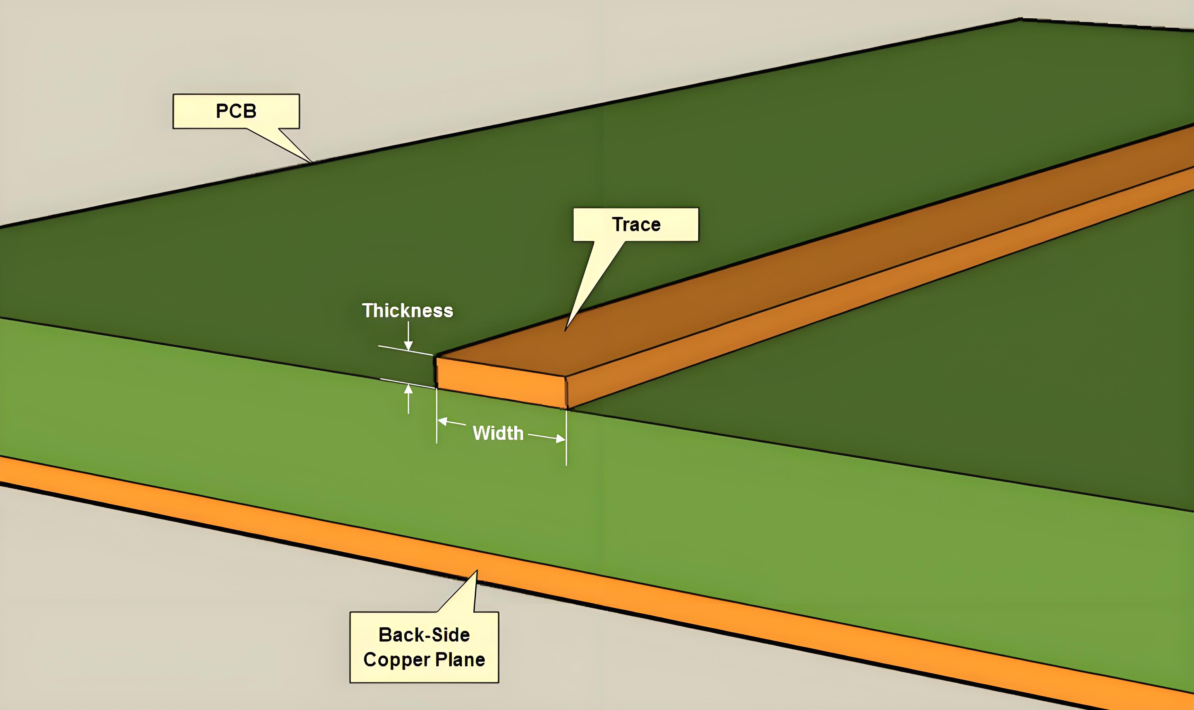
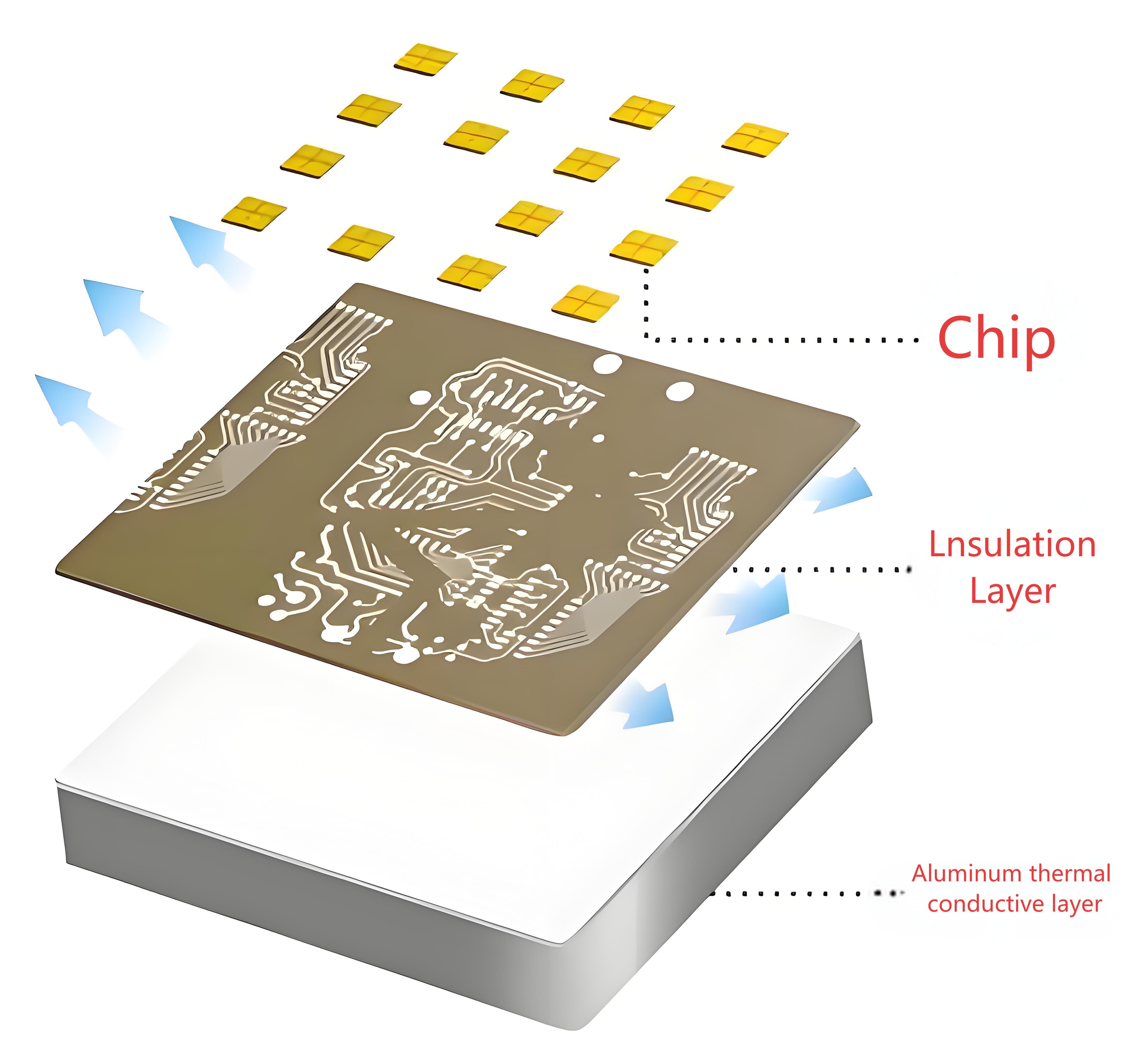
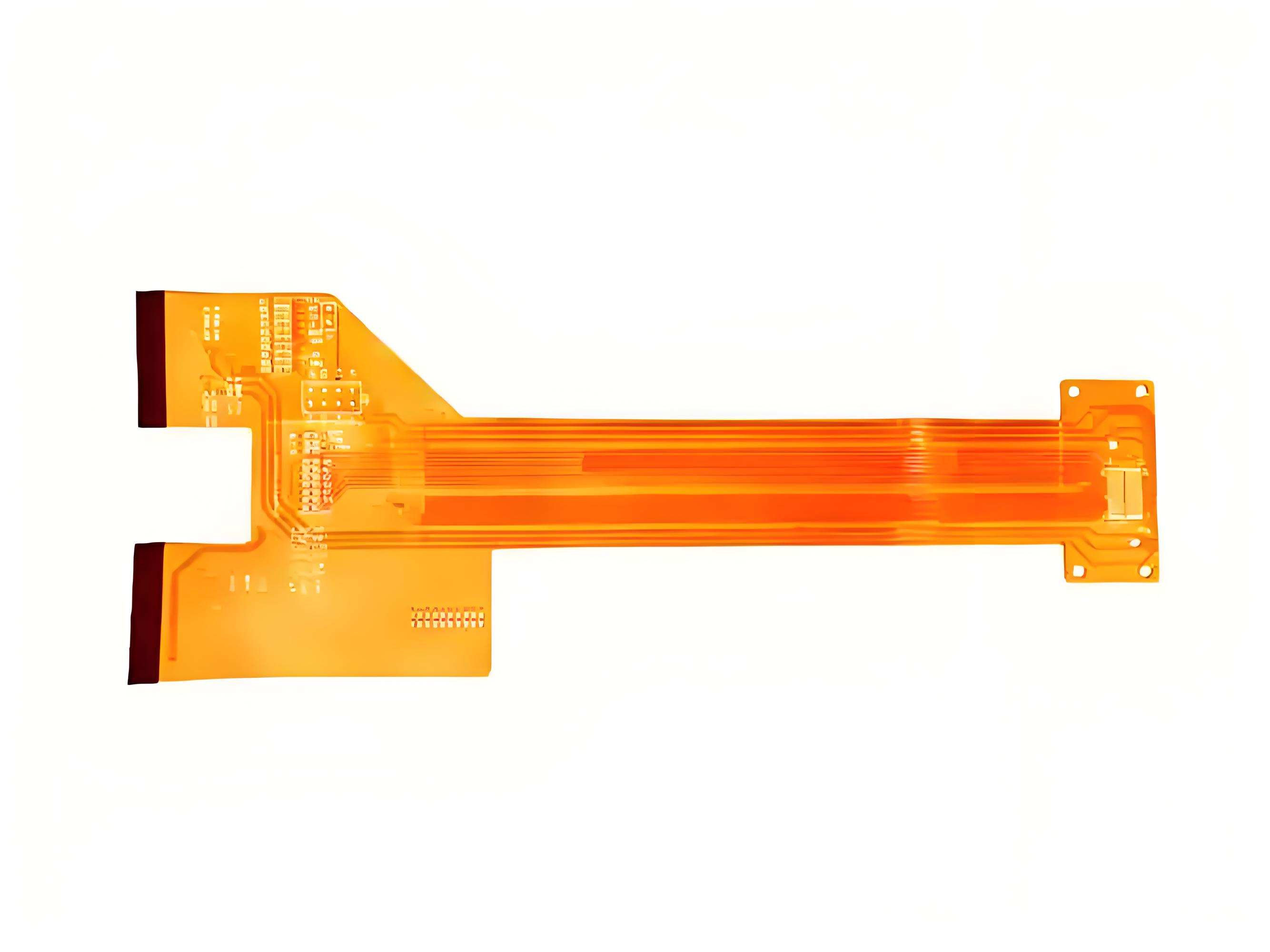
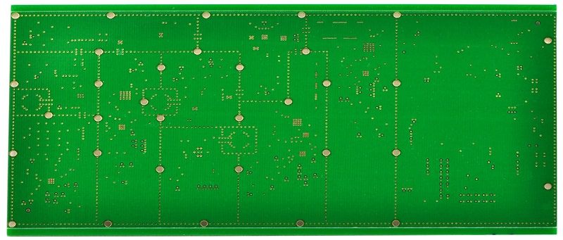
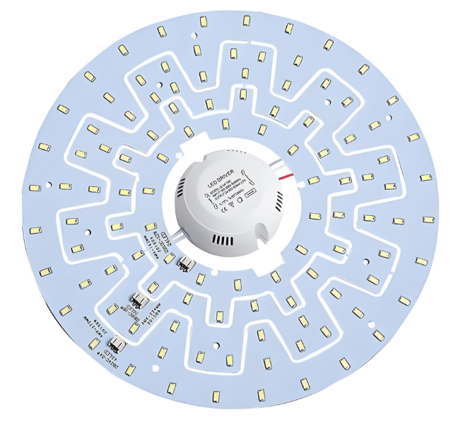
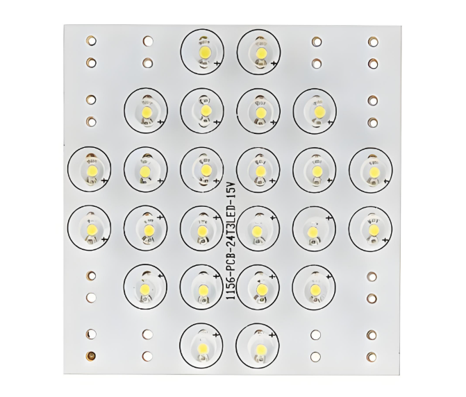
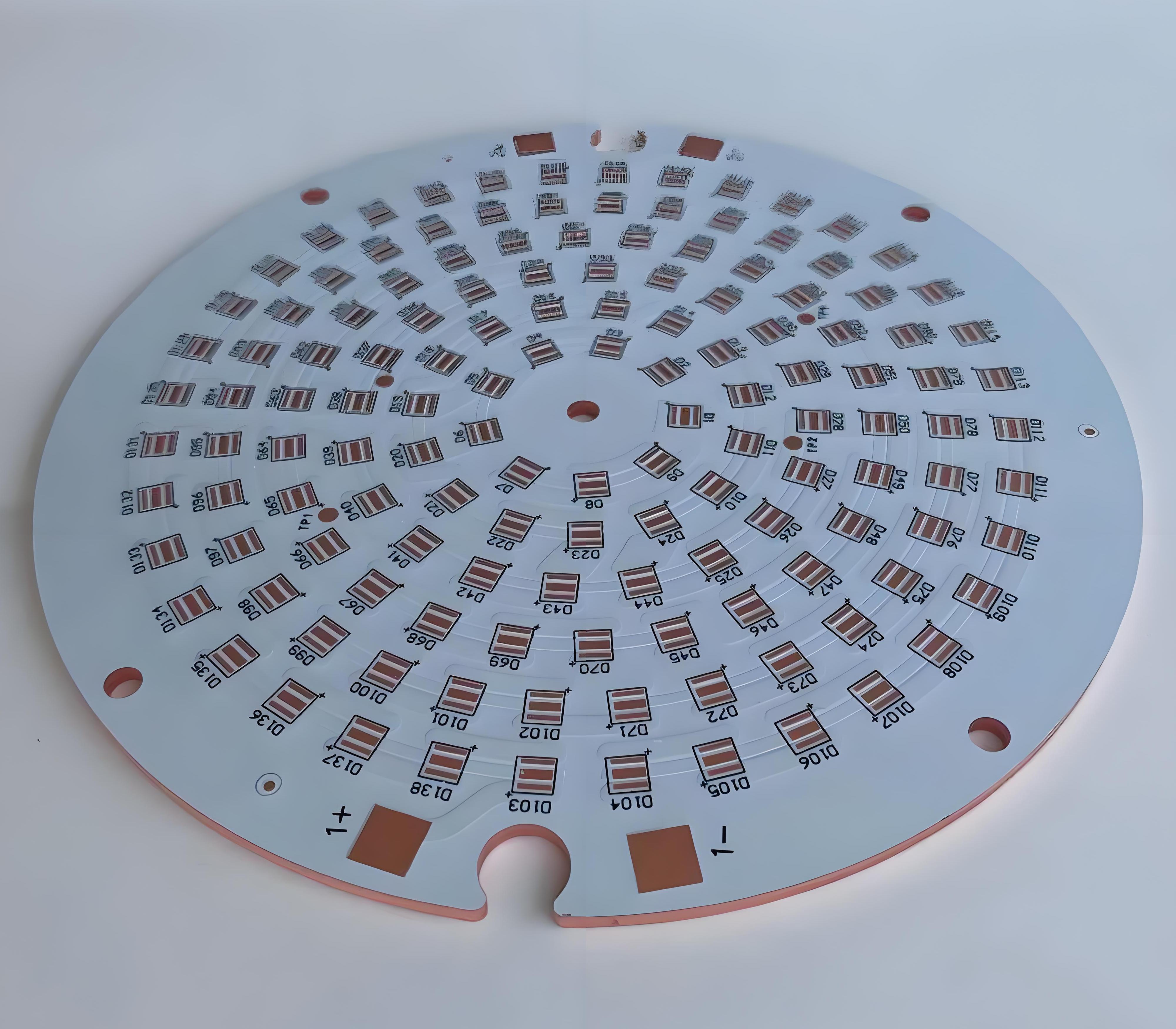
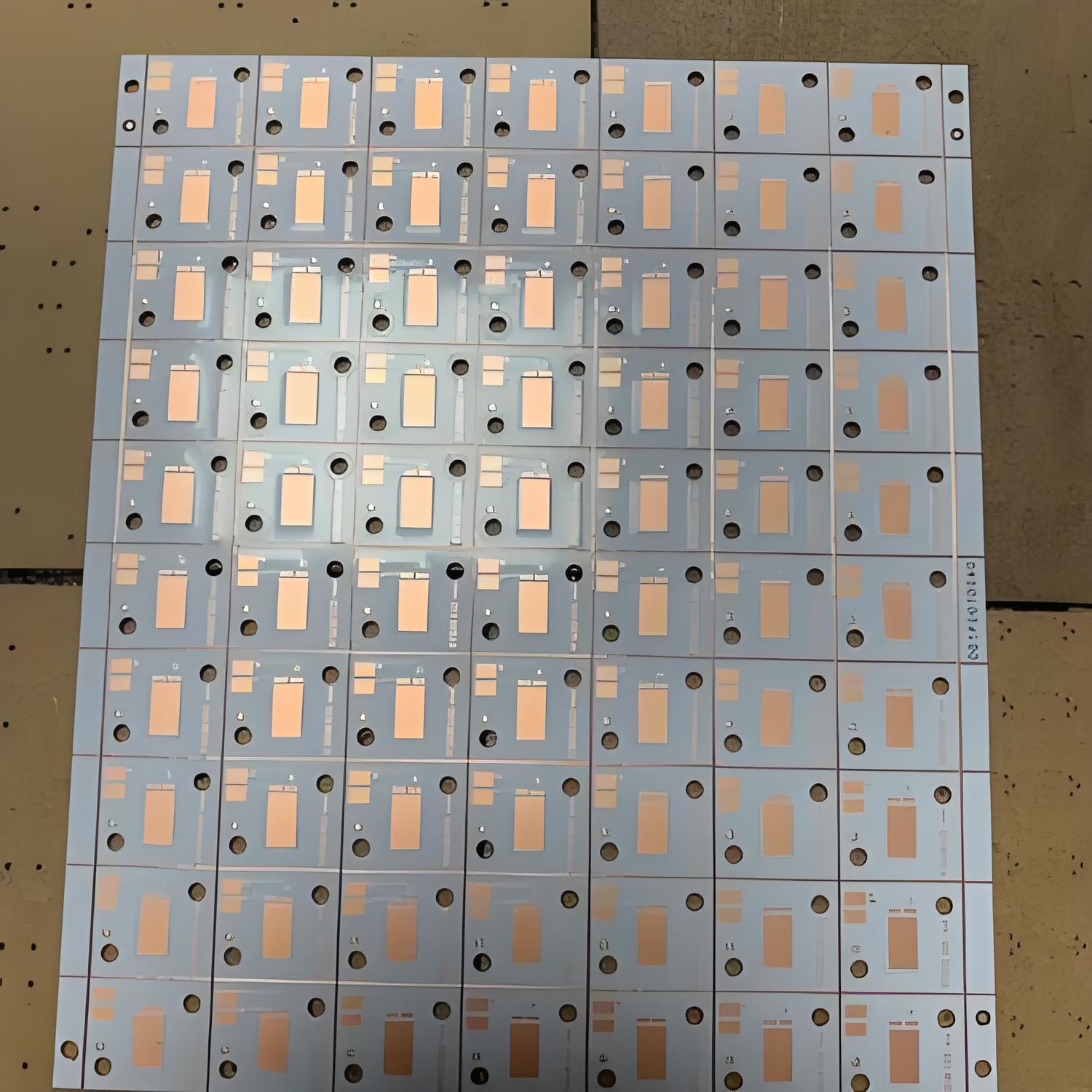
Insulated Metal Base PCB is a type of circuit board designed for high heat dissipation. It features a metal core—usually aluminum or copper—covered by a thin insulating layer and a copper circuit layer. This structure allows heat to transfer away from components quickly, making it ideal for high-power applications like LED lighting, power supplies, and automotive systems.
What is IMS in PCB?
IMS stands for Insulated Metal Substrate. It’s a specific type of printed circuit board designed to transfer heat away from high-power components.
Unlike traditional boards made of FR4 or fiberglass, IMS PCBs have a metal base layer, typically aluminum or copper. Above this, there’s a thin dielectric insulation layer that separates the metal from the copper circuitry. This structure allows the board to carry electrical signals while efficiently pulling heat away from components.
What’s the IMS PCB definition?
In simple terms, an IMS PCB is a single-layer PCB with a metal backing that provides better thermal conductivity than standard materials.
This type of board is especially common in high-power applications like LED drivers, power supplies, automotive lighting, and industrial equipment.
The insulation layer, though thin, plays a critical role. It ensures the circuit functions properly while still allowing heat to pass through to the metal core. This sandwich-like structure is what sets IMS PCBs apart from standard designs.
What materials are used in IMS board PCB production?
Here’s what goes into a high-performance IMS board PCB:
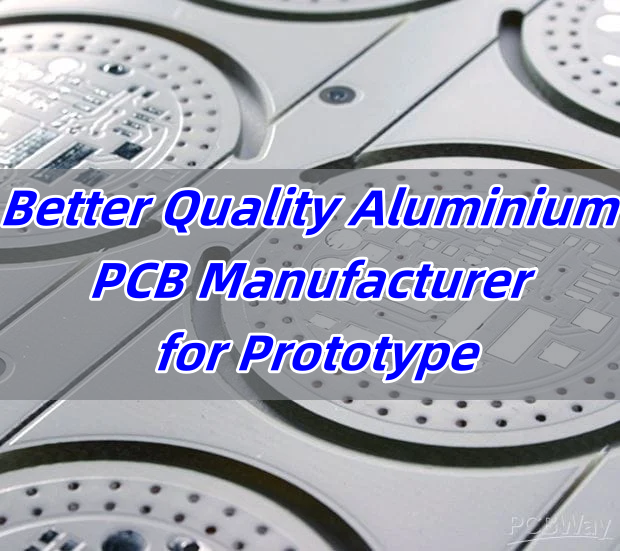
- Metal Base Layer: Most commonly aluminum, though copper is used in high-demand environments. Aluminum is preferred for its cost-efficiency, lightweight nature, and good thermal performance.
- Dielectric Layer: This is the heart of heat transfer. It must be thin enough to allow thermal flow, yet strong enough to withstand voltage stress.
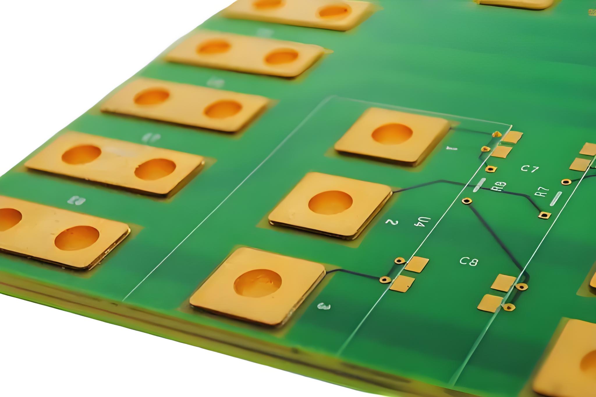
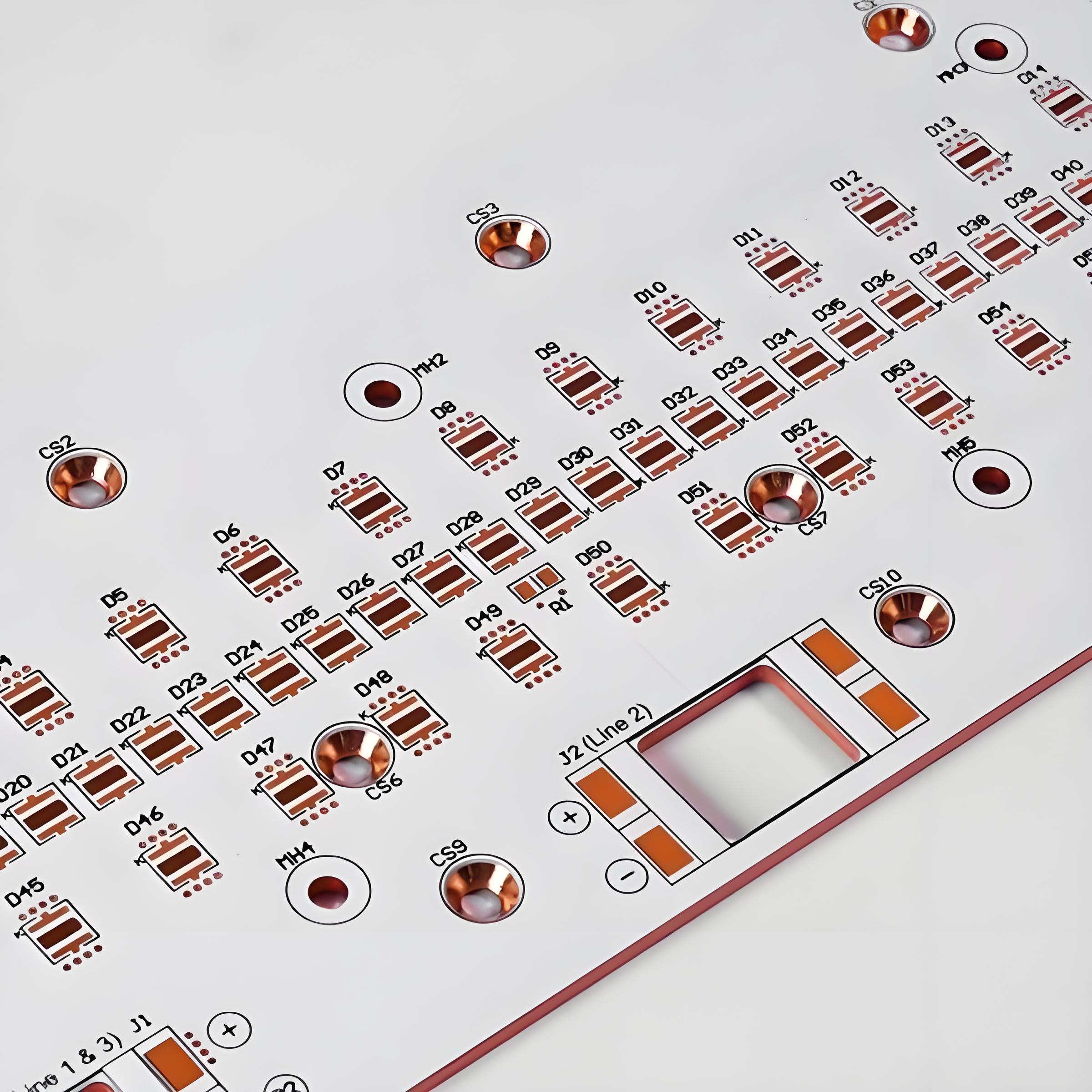
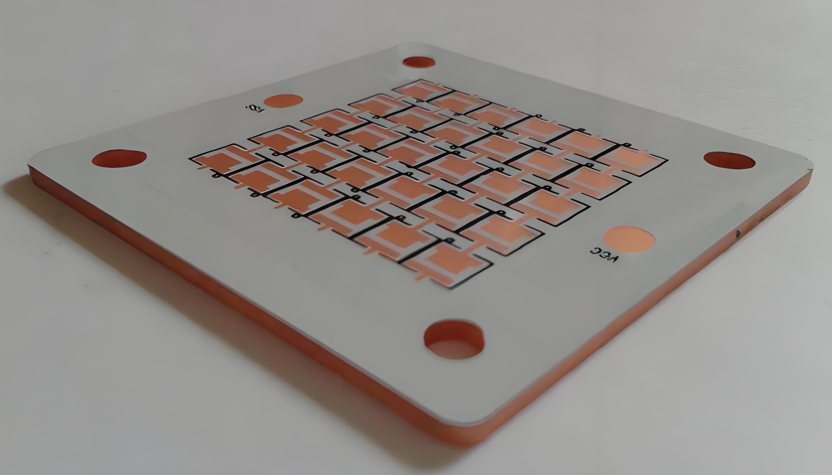
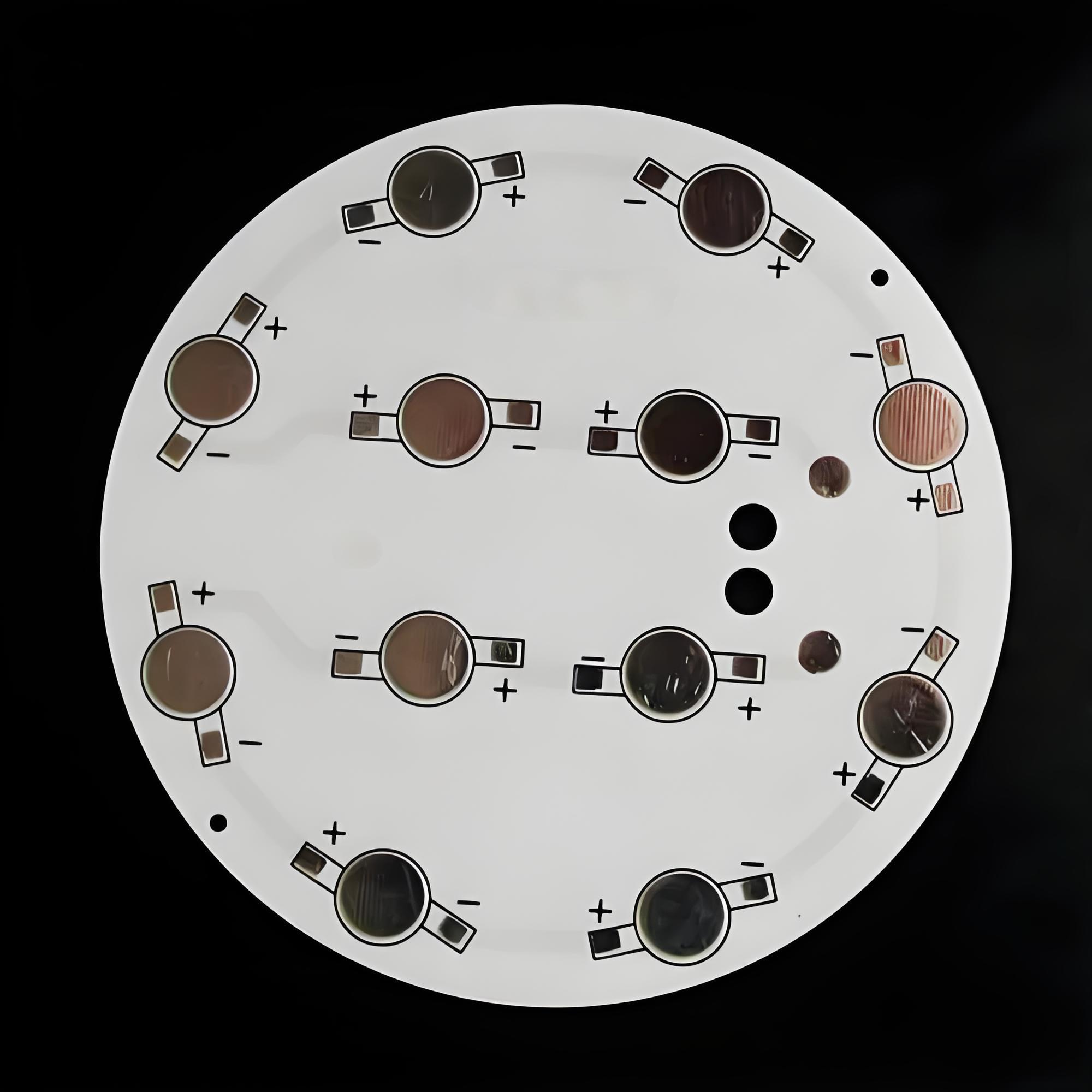
- Copper Foil Layer: The circuit layer, typically 1–3 oz thick. It’s where your electronic components connect and signals travel.
- Surface Finish: Surface treatments like ENIG (Electroless Nickel Immersion Gold) or OSP (Organic Solderability Preservatives) ensure strong soldering and prevent oxidation.
At BEST Technology, we tailor each IMS board to your exact needs. Whether you need copper or aluminum base materials, custom thicknesses, or unique finishes, we deliver to your standards.
How does IMS manufacturing work?
The IMS manufacturing process is precise and tailored. Here’s how we do it at BEST Technology:
- Base Preparation: We start with high-purity aluminum or copper plates. These are cleaned and prepped to remove any contaminants.
- Lamination: A dielectric material is laminated onto the metal base. This insulation controls both heat transfer and electrical isolation.
- Copper Cladding: A copper foil is applied on top of the dielectric. It forms the base of your circuit paths.
- Imaging and Etching: Using UV exposure, we apply your circuit pattern. Then we etch away excess copper to leave behind only your desired traces.
- Drilling and Plating: Holes for mechanical support or electrical connections are precisely drilled and plated.
- Solder Mask and Finish: A solder mask is applied, followed by a surface finish that fits your assembly method.
- Testing: Electrical testing ensures every circuit functions perfectly. Our factory performs 100% inspection before shipment.
How does IMS PCB handle heat?
The beauty of IMS PCBs lies in their thermal path. Heat from components passes through the copper trace into the dielectric layer, and from there, it’s transferred to the metal base. The base, often aluminum, quickly spreads and dissipates the heat across the board or into a heat sink.
This keeps the board cooler, even under high-power loads.
Compared to standard FR4 boards, IMS PCBs have up to 10 times better thermal conductivity. This directly reduces component stress, avoids early failure, and boosts long-term reliability.
What are the benefits of IMS PCB?
- Superior Heat Dissipation: IMS PCBs are engineered to manage heat—fast and efficiently.
- Compact Design: With better thermal control, components can be placed closer together. This allows for smaller, lighter devices.
- Longer Lifespan: Cooler components last longer. That means fewer repairs, better reliability, and a higher-quality end product.
- High Mechanical Strength: The metal base adds stiffness and reduces vibration. Ideal for automotive, aerospace, and outdoor equipment.
- Cost Savings Over Time: While slightly more expensive upfront, IMS boards can reduce the need for extra cooling systems.
- High Power Density: Great for applications like LED drivers, where compact, powerful systems are a must.
In short, IMS PCBs deliver power, durability, and efficiency—the perfect trio for demanding industries.
What is an IMS board PCB used for?
IMS PCBs are extremely versatile and can be used in systems where heat and power are a concern. Common uses include:
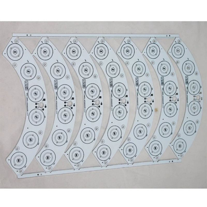
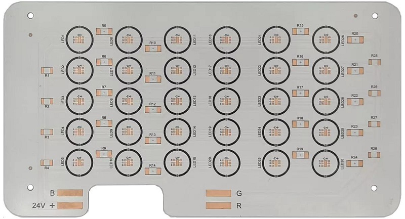
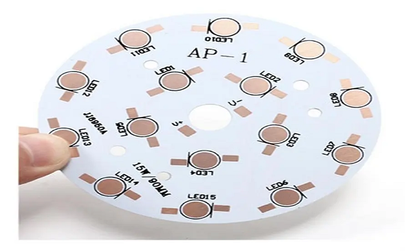
- LED lighting modules: Street lights, automotive headlights, stadium lighting.
- Power electronics: Converters, adapters, power distribution units.
- Automotive systems: Brake systems, engine control units, infotainment panels.
- Industrial control: Motor drivers, automation panels, heavy machinery.
- Medical devices: Imaging equipment, surgical lighting, diagnostic systems.
- Telecom equipment: Base stations, antennas, and signal amplifiers.
These boards shine in any place where compact size and high power must coexist safely.
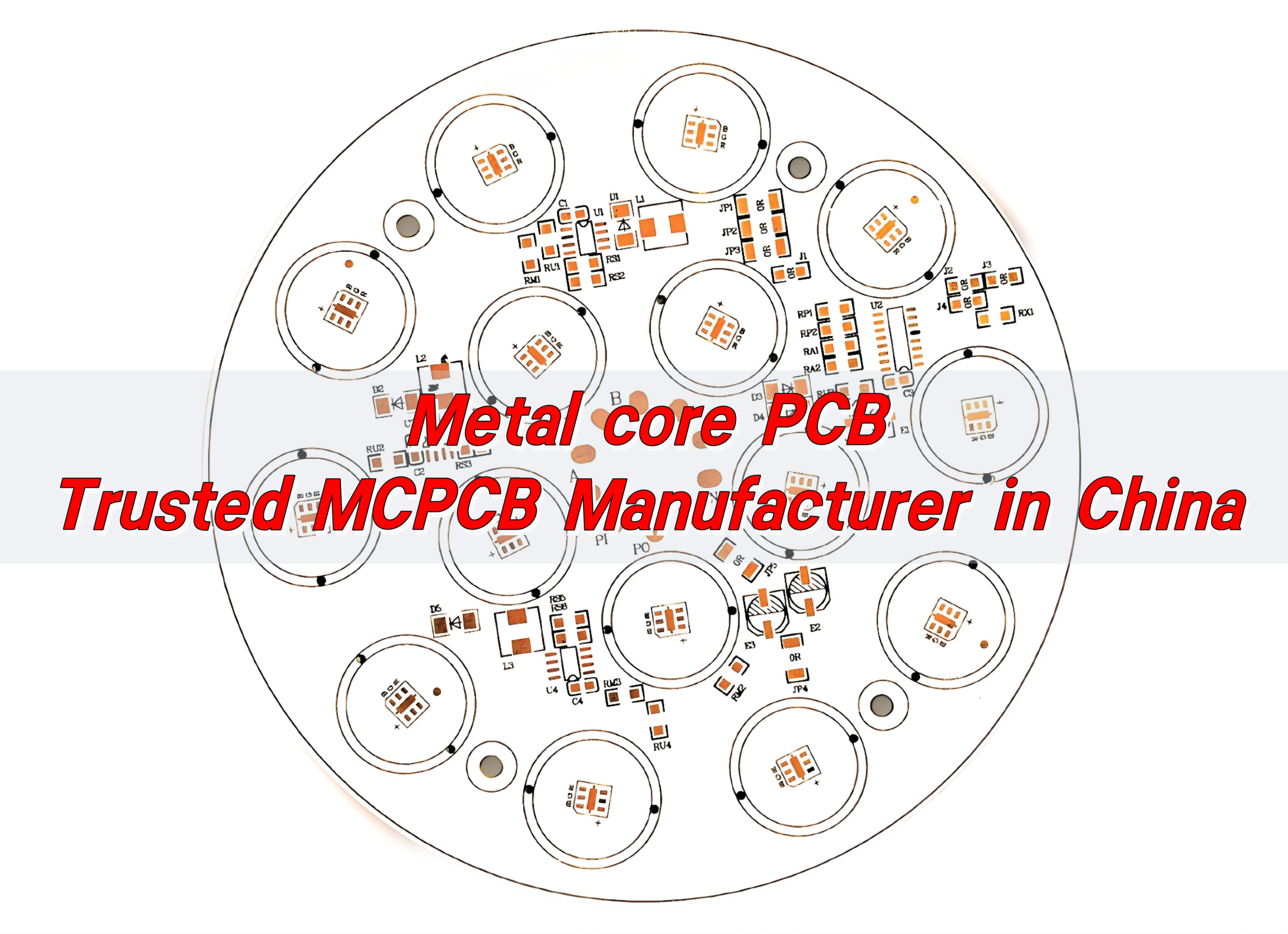
What is the best PCB manufacturer?
When you’re sourcing IMS boards, the manufacturer you choose makes all the difference.
BEST Technology stands out as one of the most reliable IMS PCB manufacturers in China. Here’s why:
- Established expertise: Since 2006, we’ve focused on MCPCBs and IMS boards, delivering quality without compromise.
- Certified reliability: We hold certifications like UL, ISO9001, ISO13485, IATF16949, and SGS—backing our quality promise.
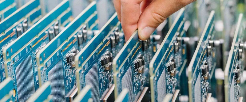
- Full turnkey service: From PCB design to assembly, we manage it all. This shortens lead times and streamlines your workflow.
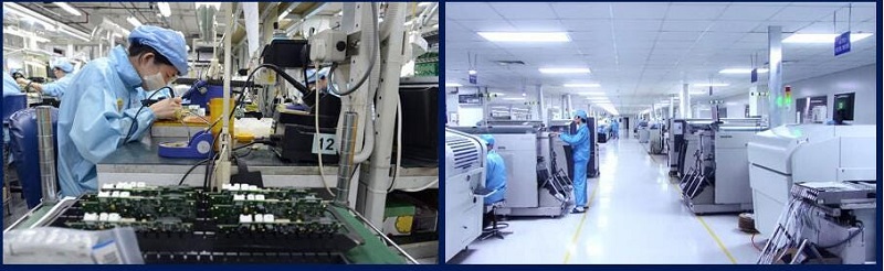
- Strong factory support: Our 30,000㎡ plant and 229+ staff allow for large-scale production with consistent results.
- Competitive pricing: We manage costs smartly to give you maximum value for your investment.
Most importantly, we believe in partnerships. Our team works closely with yours, offering one-on-one assistance, custom solutions, and a 48-hour technical response policy.
Conclusion:
Whether you’re designing compact LED modules or building industrial power units, an IMS board offers the reliability and performance you need.
As a professional IMS PCB manufacturer, BEST Technology can provide trusted expertise, service and quality. With over 19 years of experience, comprehensive certifications and a customer-first philosophy, we are proud to be a reliable supplier for all your IMS board needs.
Have a project in mind? Reach out to us today at sales@bestpcbs.com