Internal PCB Antenna is a critical component that enables compact wireless devices to achieve stable signal transmission while saving space and reducing assembly complexity. This article explains the design principles, prototyping process, and manufacturing considerations required to develop reliable Internal PCB Antenna solutions for modern electronic products.
EBest Circuit (Best Technology) is your trusted partner for end-to-end Internal PCB Antenna solutions. We design, prototype, and manufacture high-performance PCB antennas that are fully integrated into your circuit board, delivering excellent signal performance while saving valuable device space.
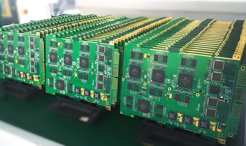
From early RF simulation to volume PCBA manufacturing, our engineering team supports the entire development process. As a result, your product can achieve stable wireless performance in demanding industries such as IoT devices, medical electronics, smart sensors, and telecommunications equipment. Pls feel free to contact us anytime at sales@bestpcbs.com to get expert support for design, prototyping, and PCBA manufacturing.
What is an Internal PCB Antenna and Why Do You Need One?
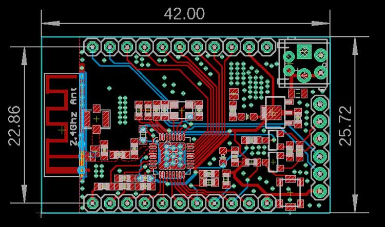
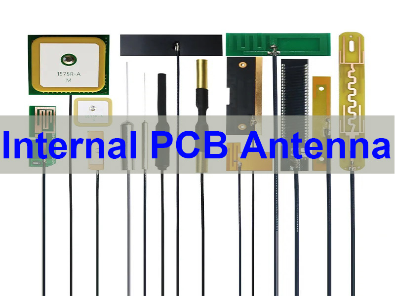
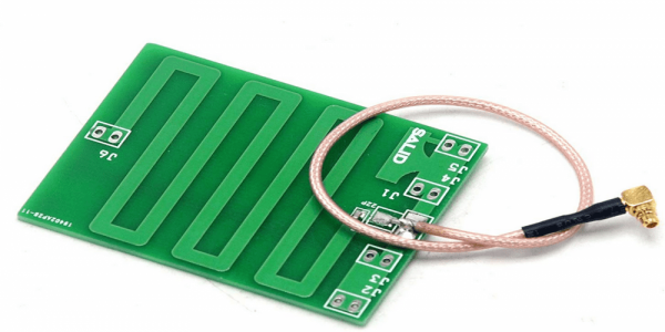
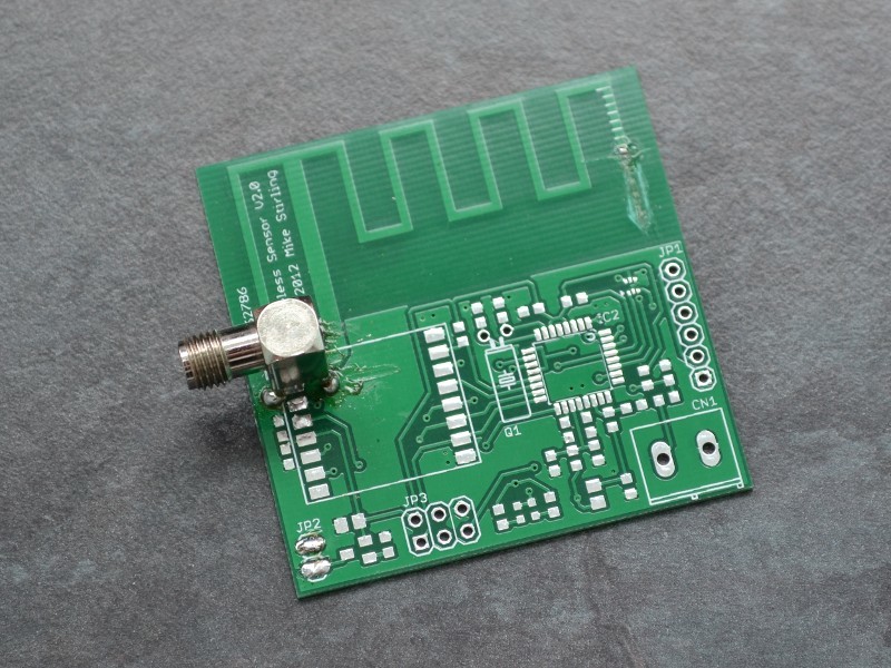
An Internal PCB Antenna is an antenna structure etched directly on the PCB copper layer. It may appear as a trace antenna, loop antenna, or patch antenna integrated within the board layout.
Unlike external antennas, internal PCB antennas do not require additional hardware components. Therefore, they simplify product structure while reducing assembly cost.
This design approach is widely used in compact electronics such as:
- IoT sensors
- wearable medical devices
- industrial monitoring equipment
- wireless communication modules
However, designing an internal antenna is not simply drawing a copper trace. Nearby components, enclosure materials, and ground planes can all influence antenna performance.
Therefore, proper design and simulation are essential to ensure reliable wireless connectivity.
In short, an internal PCB antenna allows engineers to achieve compact design, lower cost, and improved product durability.
Key Considerations for Successful Internal PCB Antenna Design
Designing a reliable Internal PCB Antenna requires careful RF engineering. Based on common discussions in technical communities, engineers often encounter several challenges.
Typical issues include:
- impedance mismatch
- ground plane interference
- signal detuning caused by nearby components
- unexpected radiation pattern changes
As a result, antenna performance may degrade significantly after integration into the final product.
At EBest Circuit (Best Technology), we address these problems through a structured RF design process.
Pre-Layout Simulation
First, we perform electromagnetic simulation to evaluate antenna performance. The simulation includes PCB stack-up parameters, dielectric constant, and board thickness.
Ground Plane Optimization
Second, we optimize the ground plane design. The ground plane acts as the antenna’s counterpoise and strongly influences radiation efficiency.
Real-World Tuning
Finally, prototypes are tested inside the actual enclosure. This allows engineers to adjust the antenna structure for the real product environment.
Therefore, proper design methodology significantly improves antenna reliability and communication stability.
From Design to Reality: The Critical Prototyping Phase for PCB Antennas
Even the best antenna simulation can behave differently in the physical world. This difference is often called the integration gap.
In practice, many prototypes experience:
- frequency shift
- reduced radiation efficiency
- lower signal range
These issues typically appear after the antenna is integrated with components and housing structures.
To eliminate this gap, EBest Circuit (Best Technology) uses an engineering-driven prototyping process.
Our prototype development includes:
- functional PCB antenna test boards
- vector network analyzer measurements
- radiation pattern evaluation
- iterative tuning adjustments
Through repeated testing and optimization, we ensure the antenna performs correctly in the final product environment.
As a result, the design moves from theoretical simulation to a reliable production-ready antenna.
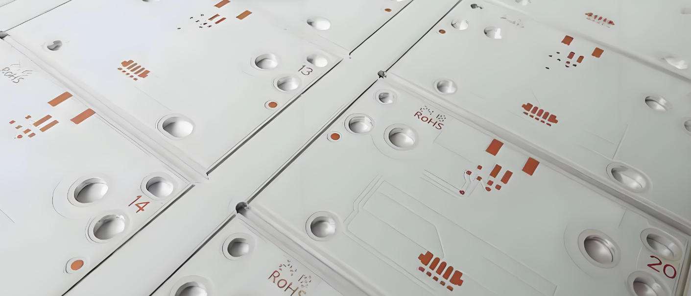
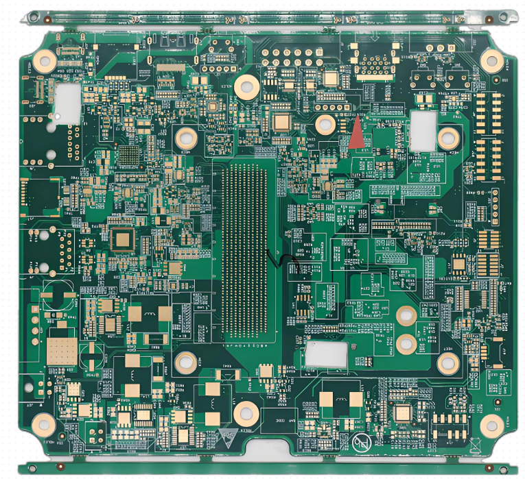
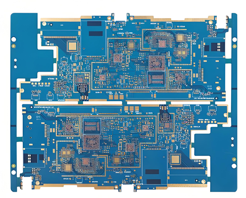
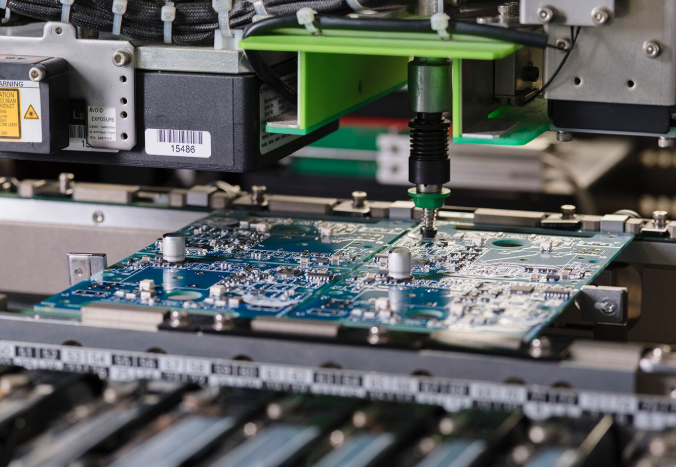
Streamlining Internal PCB Antenna Assembly for Volume Production
Once the prototype is validated, the next challenge is large-scale production.
For Internal PCB Antenna assembly, manufacturing consistency is critical. Even small variations in PCB material, trace geometry, or soldering processes can influence RF performance.
Common production risks include:
- variation in substrate properties
- inconsistent trace dimensions
- assembly interference near the antenna region
EBest Circuit (Best Technology) addresses these challenges with strict process control.
Our production capabilities include:
- automated SMT assembly lines
- controlled PCB fabrication processes
- RF-safe component placement guidelines
- selective conformal coating
As a result, every unit maintains the same antenna performance as the validated prototype.
Ultimately, this ensures stable wireless communication across large production volumes.
Why EBest Circuit (Best Technology) is the Preferred Choice for Your Internal PCB Antenna Project?
Choosing the right manufacturer is essential for any RF-based product.
Unlike traditional PCB suppliers, EBest Circuit (Best Technology) combines RF engineering expertise with advanced PCB manufacturing capability.
Our engineering team has experience designing various antenna structures, including:
- PCB loop antennas
- dipole antennas on PCB
- inverted-F antennas
- dual antennas for MIMO systems
Furthermore, we provide a complete service chain, including:
- antenna design consultation
- PCB fabrication
- prototype validation
- PCBA assembly
Therefore, customers can manage their entire antenna project through a single partner.
Ultimately, this integrated approach reduces development time and simplifies supply chain management.
How Do PCB Antennas Actually Work?
PCB antennas convert electrical signals into electromagnetic waves.
When RF current flows through the antenna trace, it creates oscillating electromagnetic fields. These fields radiate outward as wireless signals.
The antenna trace length is typically related to the signal wavelength. For example, many antennas are designed around a quarter-wavelength structure.
However, antenna performance is not determined by the trace alone. The PCB substrate, ground plane, and surrounding environment all influence the radiation characteristics.
Therefore, successful antenna design requires understanding the entire PCB structure rather than copying reference layouts.
In essence, a PCB antenna functions as a carefully tuned RF resonator integrated into the circuit board.
PCB Trace Antenna vs. Chip Antenna: Which is Better for My Design?
When designing a wireless product, engineers often choose between PCB trace antennas and chip antennas.
Below is a simplified comparison.
| Feature | PCB Trace Antenna | Chip Antenna |
|---|---|---|
| Cost | Low (no extra component) | Higher (additional BOM part) |
| PCB Area | Larger board space | Very compact |
| Customization | Highly customizable | Fixed specification |
| Design Difficulty | Requires RF tuning | Easier integration |
| Best Use | Cost-sensitive products | Very small devices |
Therefore, PCB trace antennas are typically preferred for customized RF performance and lower production cost.
Chip antennas, however, are suitable when PCB area is extremely limited.
How to Design a Reliable PCB Trace Antenna: A Step-by-Step Guide
Designing a PCB trace antenna requires a systematic workflow.
Step 1 – Define Requirements
Determine frequency band, bandwidth, and radiation pattern requirements.
Step 2 – Select Antenna Type
Choose a suitable topology such as:
- inverted-F antenna
- meandered monopole
- patch antenna
Step 3 – Perform RF Simulation
Use electromagnetic simulation tools with the exact PCB stack-up parameters.
Step 4 – Integrate With Full PCB Layout
Place the antenna inside the full circuit layout and evaluate interaction with components.
Step 5 – Prototype and Measure
Manufacture test boards and measure S-parameters and radiation patterns.
Step 6 – Tune the Antenna
Adjust trace length or geometry to reach optimal performance.
Ultimately, this iterative process ensures stable antenna behavior in the final product.
Optimizing Performance When Using Two Antennas on One PCB
Modern wireless systems often use dual antennas for diversity or MIMO communication.
However, placing two antennas on one PCB introduces mutual coupling, which can reduce signal efficiency.
To minimize interference, engineers typically apply several techniques.
Increase Antenna Separation
Whenever possible, antennas should be placed at least ¼ to ½ wavelength apart.
Use Orthogonal Polarization
Orient antennas at different angles to reduce electromagnetic interaction.
Apply Decoupling Techniques
Ground plane shaping and decoupling circuits can improve port isolation.
Optimize Ground Structure
Slots or segmented ground planes can help control RF current paths.
As a result, properly designed multi-antenna systems can significantly improve wireless communication reliability.
Common Pitfalls in Internal PCB Antenna Design and How to Avoid Them
Even experienced engineers occasionally encounter antenna design problems.
Some common mistakes include:
Ignoring the Enclosure
Plastic or metal housings can detune the antenna resonance.
Poor Ground Plane Design
An incorrect ground plane layout often leads to inefficient radiation.
Routing Signals Too Close
High-speed digital traces near the antenna may introduce noise.
Certification Oversight
Regulatory requirements such as FCC or CE testing must be considered early.
Therefore, early design review and RF testing are essential to prevent costly redesigns.
Real-World Application: Internal PCB Antennas in Medical and Aerospace Systems
Internal PCB antennas are widely used in mission-critical electronics.
Medical Devices
In wearable medical monitors, a compact PCB patch antenna ensures stable Bluetooth connectivity while maintaining a slim device profile.
Industrial and Aerospace Systems
For industrial IoT sensors installed inside metal enclosures, specialized ground plane slots allow RF signals to radiate effectively.
These examples demonstrate how customized antenna design enables reliable wireless communication even in challenging environments.
Ready to integrate a high-performance Internal PCB Antenna into your product? EBest Circuit (Best Technology) provides complete Internal PCB Antenna solutions including design consultation, rapid prototyping, and volume PCBA manufacturing. Pls feel free to contact us anytime to turn your Internal PCB Antenna design into reliable production by reaching us at +86-755-2909-1601 or sales@bestpcbs.com.
Internal PCB Antenna FAQs
How much board space does a PCB antenna require?
For a 2.4 GHz antenna, the area may range from approximately 15 mm × 5 mm for a simple trace antenna to around 25 mm × 25 mm for a patch antenna.
Can I copy an antenna design from an IC datasheet?
Reference designs are useful starting points, but they must be tuned according to your PCB stack-up and layout.
Do I need an RF engineer to design a PCB antenna?
Yes. RF design expertise is usually required to ensure reliable performance and regulatory compliance.
What is the typical gain of a PCB trace antenna?
Most PCB antennas have gains between -5 dBi and +3 dBi, depending on size and efficiency.
How can an external antenna be connected to a PCB?
External antennas typically use connectors such as U.FL or SMA, connected through a controlled-impedance 50-ohm transmission line.