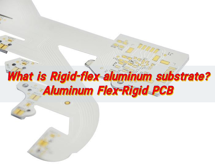
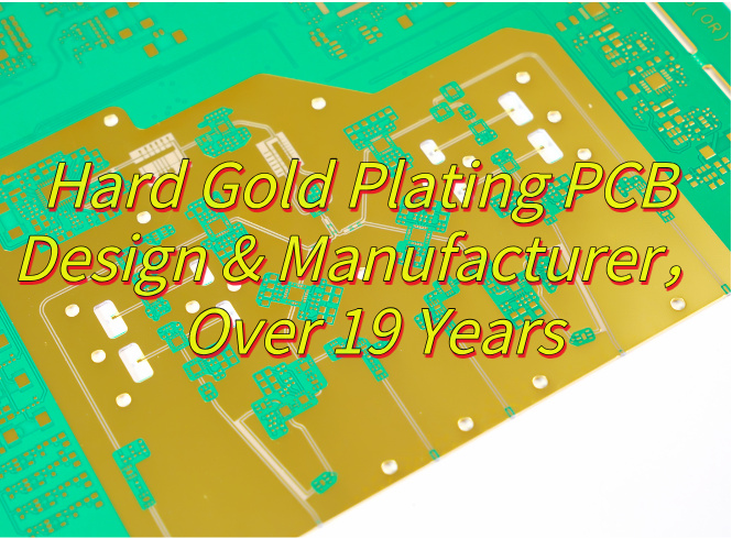
What is hard gold plating PCB? Let’s discover its definition, plating thickness, spec, benefits, applications, design guide, production process together.
Are you worried about these issues?
- Is high-frequency signal transmission loss high? (Hard Gold Plating PCB’s extremely low resistivity ensures signal integrity.)
- Is connector contact wear leading to failure? (Hard Gold Plating PCB’s wear-resistant plating has a lifespan over 5 times longer.)
- Is poor soldering causing soaring after-sales costs? (Hard Gold Plating PCB’s smooth plating achieves 100% soldering yield.)
EBest Circuit (Best Technology) can provide services and solutions:
- Customized Plating Thickness: Adjust the gold layer thickness (1-5μm) based on current load requirements to avoid excessive cost.
- Full-Process Impedance Control: Comprehensive control from substrate to plating ensures high-frequency impedance fluctuations of less than 5%.
- Mass Production Stability Guarantee: Utilizing automated plating lines and AOI quality inspection, batch-to-batch hardness variation is ≤10HV.
Welcome to contact us if you have any request for hard gold plating PCB: sales@bestpcbs.com.
What Is Hard Gold Plating PCB?
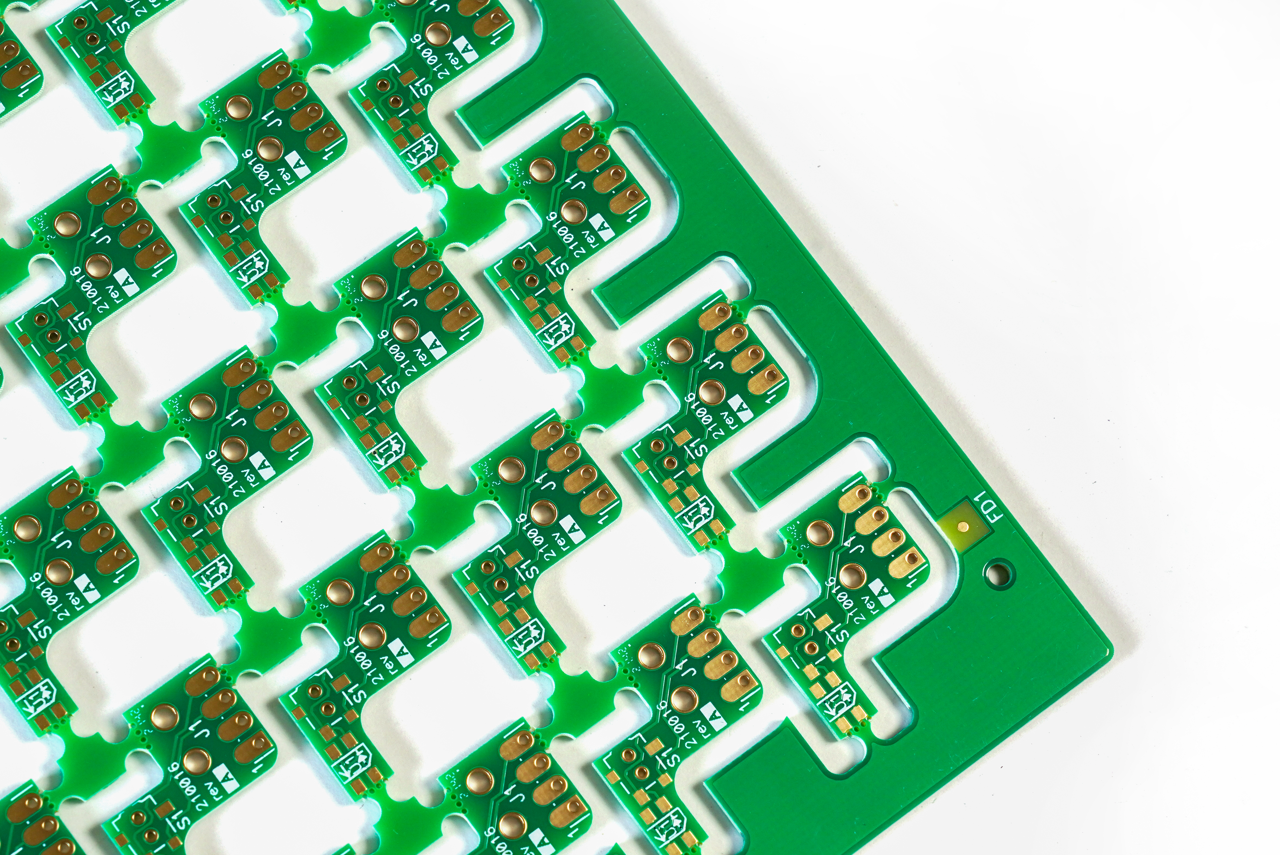
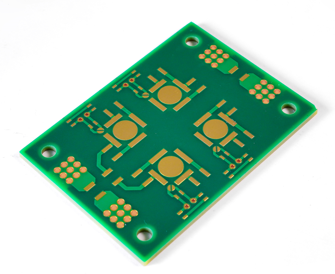
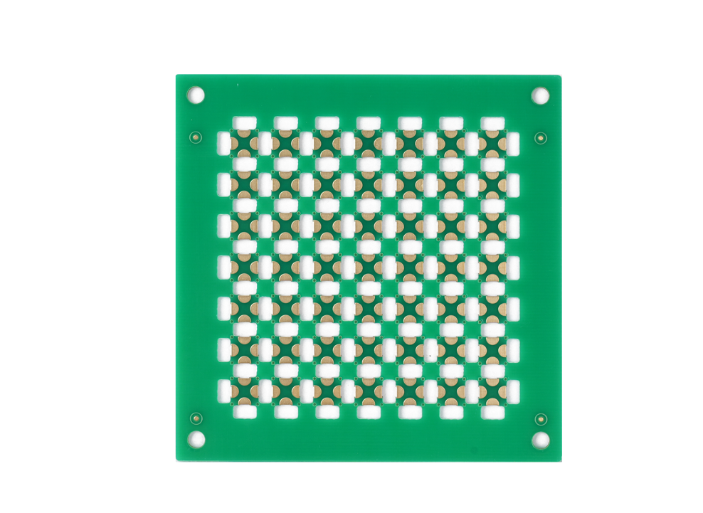
Hard Gold Plating PCB is a special process that electroplates a high-hardness gold alloy (such as gold-cobalt or gold-nickel alloy) on the surface of the PCB pads or contact points. It is characterized by the high hardness of the gold layer (150-300HV) and strong wear resistance, making it suitable for applications with frequent plugging and unplugging or mechanical friction (such as connectors, key switches, etc.).
Compared with traditional soft gold plating (pure gold), hard gold plating improves durability through the nickel base and alloy composition, but the welding difficulty is slightly higher. This process complies with industry standards (such as IPC-4552) and is a key technology to ensure the long-term reliability of high-end electronic equipment.
PCB Hard Gold Plating Thickness
PCB hard gold plating thickness is typically controlled within the range of 0.05–0.5 microns (50–500 nanometers). This thickness is precisely controlled through the electroplating process, ensuring excellent conductivity, oxidation resistance, and wear resistance (for example, gold-cobalt alloy plating can achieve a hardness of 150–300 HV), while balancing cost and soldering reliability. Too thin a thickness may result in insufficient wear resistance, while too thick a thickness increases costs and compromises soldering performance.
Hard Gold Plating PCB Specification
| Parameter | Specification |
| Gold Thickness | 0.05~0.15μm |
| Hardness | 60~120HV |
| Wear Resistance | ≥500 cycles |
| Surface Roughness | ≤0.2μm Ra |
| Adhesion | Pass Cross-cut (≥4B) |
| Solderability | IPC J-STD-003 |
| Resistivity | ≤0.05Ω·cm² |
| Operating Temp | -55℃~125℃ |
Advantages of Hard Gold Plating PCBs
- Ultra-Long-Life Design: With a hardness of 60-120 HV, its wear resistance is five times greater than soft gold, ensuring long-term, stable operation of high-frequency plug-in components (such as connectors) and reducing replacement costs.
- Guaranteed Zero Signal Loss: Resistivity ≤ 0.05Ω·cm², it’s perfectly compatible with 5G/RF modules, reducing signal attenuation and improving device communication reliability.
- Risk-Free Soldering: Passed the 100-grid test (≥4B), temperature-resistant from -55°C to 125°C, and exhibits zero delamination after soldering, making it suitable for high-reliability applications such as medical and aerospace.
- Precision Manufacturing Compatibility: Surface roughness ≤ 0.2μm Ra supports fine-pitch assembly such as BGA/CSP, improving yield and reducing production failures.
- Global Compliance: Compliant with RoHS and IPC-4552B standards, its lead-free process meets European and American environmental regulations, simplifying the export certification process.
Applications of Hard Gold Plating PCB
- High-frequency communications equipment – 5G base stations, radio frequency modules, and satellite communication systems.
- Automotive electronics – On-board sensors, ECU control units, and high-speed connectors.
- Military and aerospace – Radar systems, satellite payloads, and avionics equipment.
- Medical devices – Implantable devices, endoscopic probes, and high-precision monitors.
- Industrial automation – Robotic control panels, industrial sensors, and test probes.
Hard Gold Plating PCB Design Guide
Below is hard gold plating PCB design guide:
1. Material and Substrate Selection
- Prioritize FR-4 substrates for general applications; use low-loss materials (e.g., Rogers) for high-frequency/high-speed signals. For high-temperature or medical devices, opt for BT resin or polyimide (PI).
- Copper foil thickness: 18μm (0.5oz) to 35μm (1oz) for standard traces; ≥70μm (2oz) for high-current applications.
2. Plating Area Definition and Layout
- Restrict hard gold plating to high-wear zones (e.g., gold fingers, connector contacts, keypads). Clearly mark plating regions to avoid unnecessary costs.
- Eliminate sharp angles in plated areas; use rounded transitions (radius ≥0.3mm). Maintain ≥0.15mm (6mil) spacing between adjacent plated zones.
3. Design Rules and Parameters
- Minimum trace width/spacing: ≥4mil (0.1mm); ≥6mil (0.15mm) for dense layouts. Optimize differential traces with impedance calculators (e.g., Polar SI9000).
- Pad dimensions: Ensure pads exceed component leads (single-side extension ≥0.25mm). Use oval/oblong pads for high-density designs. Fully enclose through-hole pads; add teardrops for double-sided boards.
- Plating thickness: 1.27μm (50μin) to 2.54μm (100μin) per IPC-4552. Critical contacts (e.g., gold fingers) require ≥1.5μm for ≥10,000 insertion cycles.
4. Manufacturability (DFM)
- Define plated areas in CAD with copper overlap (minimum 500μm/20mil). Keep non-connected copper ≥800μm (31.5mil) from board edges.
- Avoid overlapping plated zones with SMT/BGA pads. Add ≥12mil (0.3mm) wide traces to gold fingers for current balance.
- Include test points for critical signals (e.g., clocks, power): diameter ≥1.8mm (70.8mil); spacing ≥2.5mm (100mil).
5. Environmental and Reliability Requirements
- Plating must pass 24-hour salt spray tests. Avoid acidic/alkaline exposure; apply protective coatings if needed.
- Reserve thermal relief for high-power zones or use metal-core substrates (e.g., aluminum). Validate material CTE to prevent delamination or pad cracks.
6. Standards and Compliance
- Plating thickness: Follow IPC-4552 (hard gold ≥1.27μm). Electrical performance: Meet IPC-6012 (Class 2/3).
- Confirm fabricator capabilities (e.g., min trace width, plating precision) upfront. Provide Gerber/drill files with clear plating annotations.
7. Testing and Validation
- Plating ductility: Pass ≥5% elongation in tensile tests. Verify thickness via XRF.
- High-speed signals: Perform TDR for impedance control. Measure contact resistance (≤50mΩ) with four-wire methods.
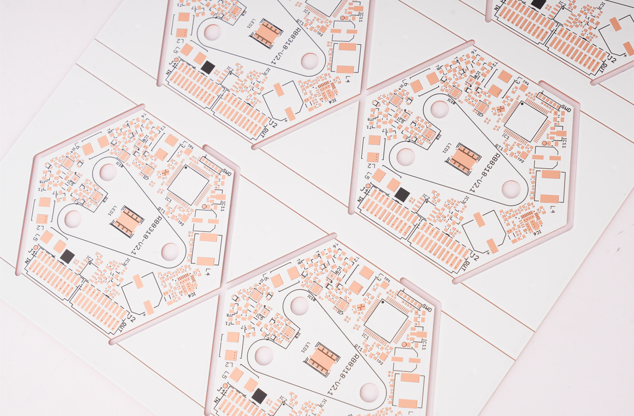
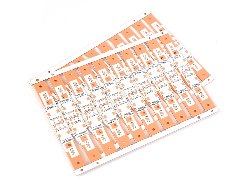
Hard Gold Plating PCB Manufacturing Process
1. Cutting
- Use a CNC cutter to cut the copper-clad laminate (e.g., FR-4) to the designed dimensions with an accuracy of ±0.1mm. Ensure smooth edges and no burrs.
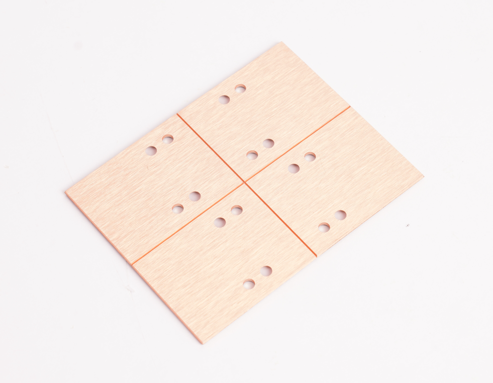
2. Drilling
- Use a CNC drill to drill holes according to the Gerber file, with diameters ranging from 0.1mm to 3mm. After drilling, clean the hole walls to remove debris and oil.
3. Inner Layer Imaging
- Clean and roughen the copper-clad laminate surface to enhance dry film adhesion.
- The inner layer circuit pattern is covered with hot press dry film (temperature 100-120°C, pressure 3-5kg/cm²).
- Use UV light exposure (energy 80-150mJ/cm²), and remove the unexposed dry film with a developer (concentration 1%-3%, temperature 30-35°C).
- Etch the unprotected copper foil with an acidic etchant (concentration 1-2 mol/L, temperature 40-50°C) to form the circuits.
4. Lamination
- The copper foil surface is treated to a tan color (thickness 0.5-1.5 μm) to enhance adhesion to the prepreg.
- The inner layer is laminated to the prepreg according to the designed number of layers, with a positioning error of ≤±0.05 mm.
- Lamination is performed at high temperature (180-220°C) and high pressure (200-400 psi) for 60-120 minutes to form a multilayer structure.
5. Hole Metallization
- The hole walls are activated using a palladium salt solution (concentration 0.1-0.3 g/L, temperature 30-40°C, time 3-5 minutes), adsorbing palladium atoms as catalytic centers.
- A copper layer is formed on the hole walls by electroless copper plating (copper sulfate 10-20 g/L, formaldehyde 5-10 g/L, pH 11-13, time 30-60 minutes).
6. External Layer Imaging
- The process is similar to the inner layer, but requires additional lead plating. Use GPM-220 antistatic gold dry film, with a secondary dry film applied only to the pad area (2 mils larger than the solder mask).
7. Pattern Plating
- Hard gold plating uses a gold-cobalt alloy (cobalt content <0.2%), while soft gold is pure gold.
- Note: Gold thickness exceeding 4 μm cannot be achieved. Pad spacing is adjusted based on the gold thickness (e.g., a 0.38 μm gold thickness requires ≥7 mils).
8. Etching
- Acidic etching solutions will corrode unprotected copper foil to ensure trace accuracy.
9. Solder Mask & Screen Printing
- Apply photosensitive solder mask ink, then expose and develop it to form a protective layer (20-50 μm thick).
- Screen-print component identification; the ink must be abrasion-resistant and corrosion-resistant.
10. Hard Gold Plating
- Full-board plating: Dry film protects the non-plated areas, with secondary dry film applied only to the window pads.
- Localized plating: Lead design (e.g., 12mil-wide traces) with dummy gold fingers to isolate current and prevent thickness variations.
11. Outline Processing & Testing
- Using V-cut or milling technology, create the PCB outline with a tolerance of ±0.1mm.
- Electrical testing (conductivity, insulation), impedance testing (according to design requirements), and environmental testing (high temperature, high humidity, high temperature).
12. Final Inspection
- Appearance inspection (no scratches or oxidation).
- Dimensional measurement (error ≤ ±0.1mm).
- Gold thickness testing (Knoop hardness ≥90) and adhesion testing.
Why Choose EBest Circuit (Best Technology) as Hard Gold Plating PCB Manufacturer?
Reasons why choose us as hard gold plating PCB manufacturer:
- Extremely Fast Delivery Guarantee: Urgent orders are processed within 24 hours, precisely meeting the urgent project delivery needs of the electronics industry and ensuring the timeliness of critical equipment R&D or repair.
- Strict Quality Control System: Full-process inspection is implemented for batch orders, ensuring a gold plating thickness tolerance of ±5% and a defect rate of less than 0.1%, ensuring highly reliable connections and long-term corrosion resistance.
- 19 Years of Technology: Leveraging 19 years of experience in precision circuit manufacturing, we efficiently address complex issues such as exposed copper in the hole wall and blackened gold surface during the gold plating process, ensuring plating uniformity and adhesion.
- Transparent Cost Optimization: Utilizing a no-hidden-cost pricing model combined with automated process optimization, we achieve cost savings of 15-20% compared to the industry average, making it particularly suitable for small and medium-volume orders.
- Free DFM Design Optimization: Free Design for Manufacturability (DFM) analysis is provided to proactively avoid issues such as improper gold plating area design and solder mask window errors, reducing rework costs by up to 30%.
- High First-Time Pass Rate Guarantee: 98% of samples pass customer acceptance on the first test, reducing iterative revisions due to substandard gold plating thickness or soldering performance issues, saving time and money.
- 24/7 Technical Response: 24/7 real-time support from our engineering team quickly resolves unexpected issues during the gold plating process, such as oxidation and micro-shorting, ensuring production continuity.
- Flexible Measurement Capability: Supports small-batch prototype verification of 1-10 units to large-scale production of over 10,000 units, meeting the full cycle from R&D prototyping to mass production.
- Global Standard Compliance: Complies with international standards such as IPC-6012, UL 94V-0, and RoHS. The gold plating layer has passed ASTM B488 salt spray testing, ensuring compliance for high-end applications in medical, aviation, and other fields.
- Compatible with various post-processing processes: In addition to hard gold plating, multiple surface treatment options such as HASL, ENIG, OSP, and immersion silver are also available to meet the needs of different welding processes (such as high-frequency signal transmission, high-precision placement, etc.).
Welcome to contact us if you have any inquiry for hard gold plating PCB: sales@bestpcbs.com.