PCB manufacturing Cape Town is the localized production of circuit boards that supports fast prototyping, reliable builds, and smooth development for electronics teams in the region. This guide explores Cape Town’s top-tier PCB manufacturing ecosystem, explaining why it’s a strategic hub for innovation and how to navigate your options.
What are the key pain points teams face when sourcing PCBs?
- Lengthy lead times and delays: Overseas prototypes arrive too slowly and slow down iteration.
- Inconsistent quality and hidden defects: Flawed boards cause failed tests and extra rework.
- Unpredictable and rising total cost: Unexpected fees push projects beyond budget.
- Weak communication and support: Time zones and language gaps slow urgent DFM discussions.
- Limited capability for complex builds: Local PCB manufacturer options often cannot support HDI or controlled impedance.
The solution lies in partnering with a capable, local PCB partner. A trusted PCB factory in Cape Town directly addresses these challenges by providing integrated support. Here’s how:
- Dramatically Faster Turnarounds: Prototypes move from days, not weeks.
- Guaranteed Quality with Proximity: Local oversight keeps yields stable.
- Transparent and Competitive Pricing: Clear costs without surprise fees.
- Seamless Collaboration: Same-zone support speeds DFM feedback.
- Access to Advanced Technical Expertise: Local teams guide complex builds.
Among the leading Chinese PCB providers, BEST Technology is one of the top PCB Manufacturers South Africa partner for both standard and advanced projects. We specialize in fast-turn, high-quality PCB fabrication and assembly, serving as a reliable cornerstone for South Africa’s electronics sector. Our expertise ensures your design moves seamlessly from file to finished board. For a direct quote or technical consultation, pls feel free to contact us at sales@bestpcbs.com.
Why PCB Manufacturing Cape Town Supports Faster Innovation for Local Electronics Teams?
Local PCB manufacturing Cape Town is a catalyst for rapid innovation. Proximity enables an agile development cycle that is impossible with distant suppliers.
- Speed of Iteration: Engineers can submit design revisions and receive new prototypes within days. This “fail fast, learn fast” approach accelerates product development.
- Ease of Collaboration: Face-to-face meetings or quick site visits facilitate deep technical discussions about DFM, materials, and testing protocols.
- Supply Chain Resilience: Reducing dependence on international logistics minimizes risk from global disruptions, ensuring a more reliable component of your PCB production process.
For local teams, a Cape Town-based partner transforms the prototyping phase from a bottleneck into a competitive advantage.
How PCB Manufacturing South Africa Builds a Strong National Supply Chain for Engineering Projects?
A robust PCB manufacturing South Africa infrastructure strengthens the entire national electronics sector. It creates a dependable foundation for everything from startups to large-scale industrial projects.
- National Resource Integration: It leverages local talent, raw material supply chains, and logistical networks, keeping value and expertise within the country.
- Economic & Strategic Benefits: Building PCB manufacturing capabilities locally supports job creation, reduces import costs, and enhances national technological sovereignty.
- Unified Standards: Working within a national framework helps standardize quality and certification processes across projects.
Investing in South Africa’s PCB industry is an investment in a stable, self-reliant engineering future.
How PCB Manufacturing Johannesburg Compares to Cape Town?
South Africa’s PCB industry develops along two distinct strengths. Johannesburg serves as the country’s logistics and assembly hub, while Cape Town is recognized for advanced PCB fabrication and high-precision engineering work. The comparison below highlights how these two centers differ in focus, capability, and industrial relevance.
| Category | Johannesburg | Cape Town |
|---|---|---|
| Primary Role | High-volume assembly & logistics | Advanced PCB fabrication & R&D |
| Industry Focus | Consumer electronics, mining, defense assembly | Aerospace, medical, high-tech electronics |
| Key Strength | Large SMT capacity; rapid assembly | HDI, multilayer, rigid-flex, high-reliability builds |
| Representative Company | ExpandoWorks (SMT leader) | ICAPE Trax (most advanced PCB fab in SA) |
| Best For | Fast assembly and scalable production | Complex prototypes and precision boards |
What Sets Johannesburg Apart
- Strong SMT assembly capabilities, including high-speed placement for large volumes.
- Ideal for consumer electronics and contract manufacturing.
- Excellent logistics infrastructure for moving components and finished goods quickly.
What Makes Cape Town the Technical Leader
- Home to South Africa’s most advanced PCB fabrication facility, ICAPE Trax.
- Specialized in multilayer, HDI, rigid-flex, and high-reliability designs.
- Trusted for aerospace, medical, and scientific projects requiring tight tolerances.
All in all, Johannesburg is the better choice for high-volume SMT assembly and logistics-driven production, while Cape Town remains the preferred destination for complex PCB fabrication and engineering-grade prototypes. Most teams divide work accordingly: Johannesburg for speed and volume, and Cape Town for precision and technical depth.
Why Engineers Work With PCB Manufacturing Pretoria for Prototyping?
Engineers often rely on PCB manufacturing Pretoria for fast, reliable prototype development because local partners provide shorter iteration cycles, clearer communication, and more predictable quality throughout early design stages.
- Faster prototyping cycles
Local factories deliver quick-turn boards within 24–48 hours, reducing delays linked to overseas shipping. - Real-time DFM communication
Direct access to engineering teams speeds up troubleshooting and improves design accuracy early in the process. - Lower overall prototyping cost
Eliminates import duties and long-distance freight while reducing material waste through optimized paneling. - Higher first-pass success rates
Pretoria facilities apply AOI and flying-probe testing to validate prototypes before scaling. - Improved supply chain visibility
Local sourcing and easier oversight strengthen traceability for regulated industries. - More streamlined development workflow
Prototyping moves faster when design and manufacturing operate within the same region.
By partnering with PCB manufacturing Pretoria, engineers gain a faster, more controlled path from concept to validated prototype, helping projects advance with greater confidence and efficiency.
Top Rated PCB Manufacturing Cape Town
Here are the top-rated PCB manufacturers in Cape Town, evaluated based on industry reputation, technical capabilities, and local market presence. These companies range from global-standard PCB producers to specialized local fabrication and assembly facilities.
Top 10 PCB Manufacturing Cape Town
| Rank | Manufacturer | Location | Rating / Status |
|---|---|---|---|
| 1 | Cirtech Electronics | Tokai, CT | ⭐⭐⭐⭐⭐ (Global Standard) |
| 2 | Bosco Printed Circuits | Beaconvale, CT | ⭐⭐⭐⭐ (Established Legacy) |
| 3 | Trax Interconnect | Cape Town (ICAPE Group) | ⭐⭐⭐⭐ (ISO Certified) |
| 4 | Procircuit | Beaconvale, CT | ⭐⭐⭐⭐ (Contract Mfg) |
| 5 | Central Circuits | Cape Town | ⭐⭐⭐⭐ (Versatile) |
| 6 | W.H. Circuit CC | Wetton, CT | ⭐⭐⭐ (Local Fabricator) |
| 7 | Ashdan Electronics | Cape Town | ⭐⭐⭐ (PCB Assembly + Light Fabrication) |
| 8 | Master Circuits | South Africa (Servicing Cape Town) | ⭐⭐⭐ (Multilayer Specialist) |
| 9 | Zyteq | South Africa | ⭐⭐⭐ (Automation + PCB Services) |
| 10 | Jemstech | South Africa | ⭐⭐⭐ (EMS + PCB Assembly) |
Cirtech Electronics – The Market Leader
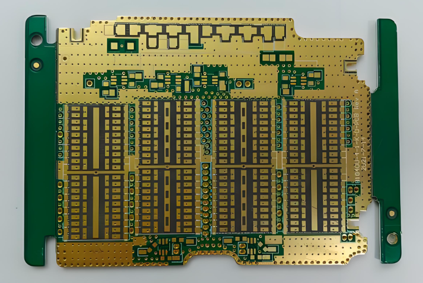
Cirtech is widely regarded as the premier PCB manufacturer in South Africa. They offer RF boards, HDI (High Density Interconnect), multilayer PCBs, and support rapid prototyping to mass production. ISO 9001 certification further demonstrates consistent quality across industries such as aerospace and defense.
Technical Specifications Comparison
| Feature | Cirtech | Trax | Bosco |
|---|---|---|---|
| Layers | 2 – 30+ (Advanced) | 2 – 20 | 2 – 20 |
| Min Drill | 0.075mm (Laser) | Standard Drilling | Standard Drilling |
| Materials | FR4, Rogers, Teflon | Standard FR4 | Standard FR4 |
| Finish | ENIG, Immersion Tin | HASL, OSP | HASL, OSP |
Note: While “Top 10” rankings vary across directories, these companies consistently appear due to their certifications, longevity, and technical capabilities.
Detailed Profiles
1. Cirtech Electronics – The Gold Standard
- Specialty: RF PCBs, HDI, Multilayer Boards
- Why choose: Trusted across aerospace, defense and industrial markets
- Location: Unit F, 12 Stibitz Street, Westlake Business Park 2, Tokai
2. Trax Interconnect – The Pioneer
- Specialty: Prototype and standard manufacturing
- Why choose: Part of the ICAPE Group, recognized globally for precision sample manufacturing
- Location: Cape Town
3. Bosco Printed Circuits – The Veteran
- Specialty: Aluminum-based PCBs, automotive-grade boards
- Why choose: Founded in 1956; reliable and cost-efficient
- Location: Beaconvale
Decision Guide: Which Manufacturer Fits Your Needs?
For Complex Projects
- Recommended: Cirtech
- Best for: High-density, RF, or multilayer PCBs
- Strengths: Advanced HDI capability, reliable performance
- Consideration: Costs may be higher for small prototype runs
For Fast Prototyping
- Recommended: Trax Interconnect or Procircuit
- Best for: Quick-turn prototypes and small volumes
- Strengths: Competitive pricing and short lead times
- Consideration: Limited support for very large mass-volume production
What is PCB Board Price South Africa?
The PCB board price South Africa is not a fixed number but a variable based on multiple factors. Key determinants include:
- Board Specifications: Size, layer count, material, copper weight, and surface finish.
- Order Quantity: Unit cost drops significantly with volume due to amortized setup costs.
- Turnaround Time: Expedited services incur higher costs.
- Special Processes: Impedance control, blind/buried vias, or gold plating add cost.
A local manufacturer can provide the most accurate and transparent PCB cost, factoring in all these elements without hidden international fees.
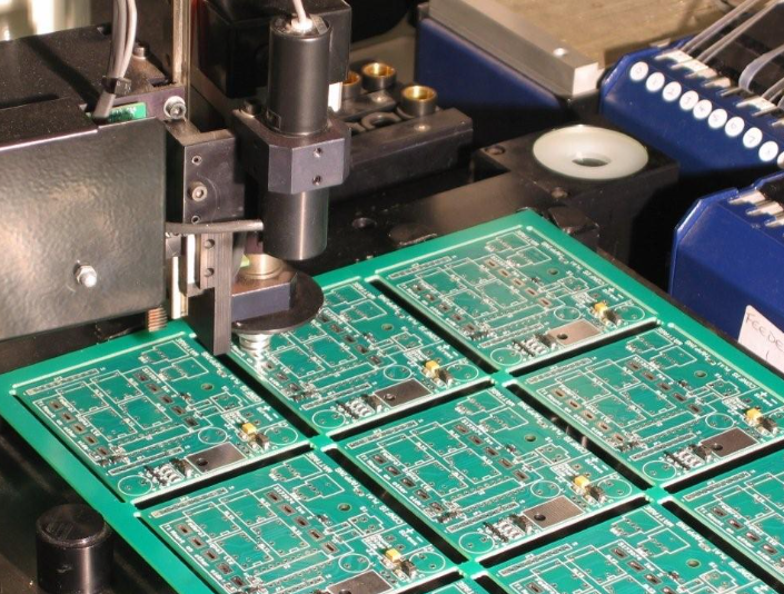
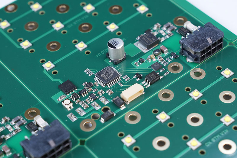
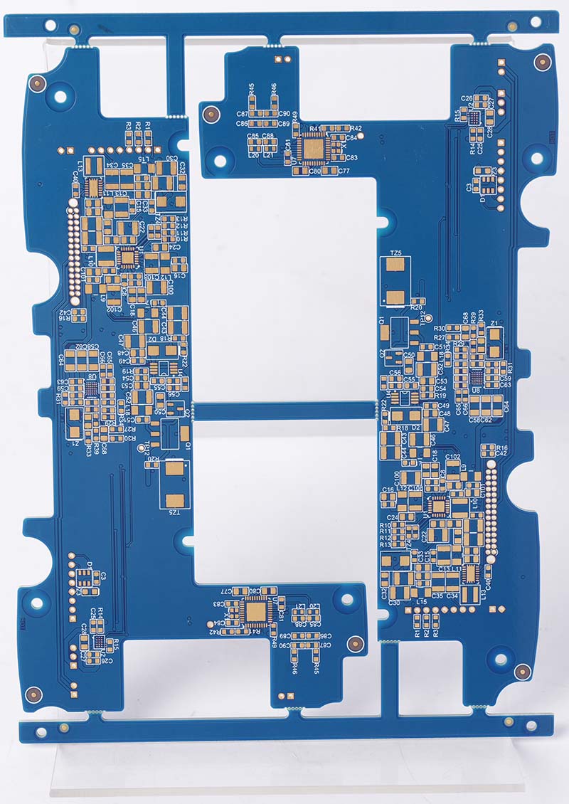
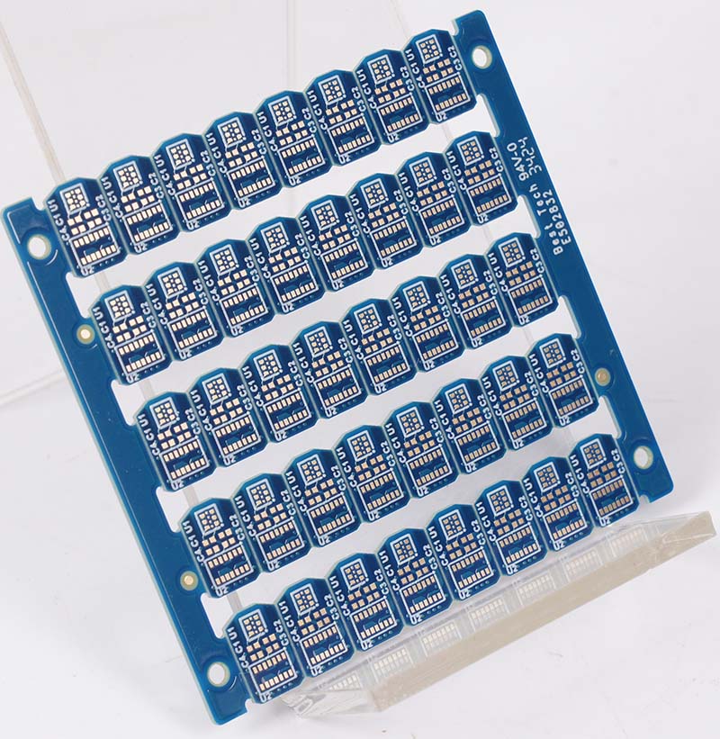
What is PCB Manufacturing Machine in Production?
The PCB manufacturing machine refers to the specialized equipment used in the PCB manufacturing process. Key machines include:
- Direct Imaging Systems: For precise pattern transfer onto panels.
- Automated Optical Inspection (AOI): Critical for catching defects early.
- Laser Drills: For creating micro-vias in HDI boards.
- Plating Lines: For copper deposition and final surface finishes.
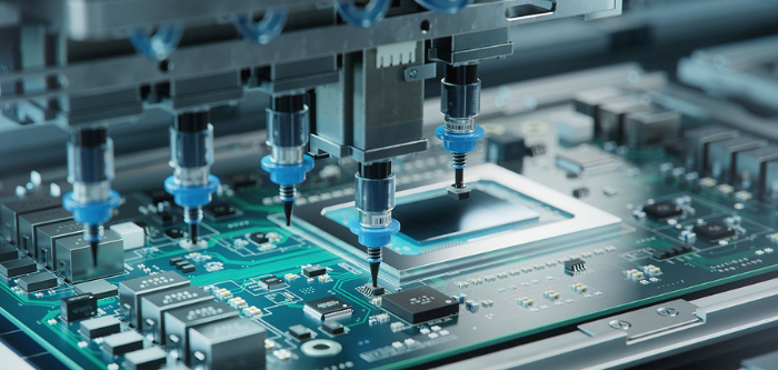
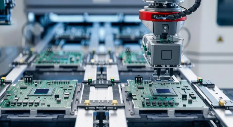
- Solder Paste Printers & Pick-and-Place Machines: Essential for the assembly stage.
The sophistication of these machines directly defines a factory’s PCB manufacturing capabilities and the complexity of boards they can produce.
How PCB Assembly Cape Town Helps Control PCB Cost?
Local PCB assembly Cape Town is a strategic tool for PCB cost control beyond just the bare board.
- Reduces Logistics & Import Overheads: Combining fab and assembly in one location eliminates multiple international shipments and handling.
- Minimizes Inventory Risk: Local assembly allows for just-in-time component procurement, reducing capital tied up in inventory.
- Prevents Costly Rework Delays: Immediate access to the assembly line allows for quick corrections, avoiding weeks of downtime from shipping boards overseas for assembly.
- Optimizes Design for Assembly (DFA): Early collaboration with the assembly house can identify and eliminate design features that are expensive to assemble.
What Leading PCB Manufacturing Companies Offer for Complex PCB Builds in South Africa?
Leading PCB manufacturing companies differentiate themselves by handling complex projects that go beyond standard FR-4 boards.
- Advanced Technologies: Expertise in HDI, rigid-flex, heavy copper, and high-frequency materials.
- Stringent Process Control: Implementing exacting standards for impedance control, plating uniformity, and reliability testing.
- Full-Turnkey Solutions: Managing the entire supply chain from component sourcing to final box-build assembly.
- Certifications & Traceability: Maintaining certifications for automotive (IATF 16949) or aerospace standards, with full material traceability.
How to Find a Reliable PCB Manufacturing Cape Town Address and Contact Number?
Finding a reliable PCB manufacturing Cape Town address and contact number is about more than just a directory listing.
- Industry Directories & Associations: Check local engineering and electronics industry bodies.
- Peer Recommendations: Leverage networks at tech meetups or university engineering departments.
- Online Research & Reviews: Search for companies with detailed websites showcasing their capabilities and client testimonials.
- Direct Engagement: The best test is to contact them with a specific technical inquiry.
Their responsiveness and expertise will be immediately apparent. If you would like to look for Chinese PCB Manufacturers supporting your PCB manufacturing South Africa projects, for instance, you can start your search with a proven Chinese PCB provider like BEST Technology at sales@bestpcbs.com.
Why EBest Circuit (Best Technology) is the Right Path for Your PCB Manufacturing South Africa Projects?
Choosing the right manufacturing partner is crucial for the success of your electronics projects. EBest Circuit (Best Technology) combines nearly two decades of expertise with a flexible, customer-centric approach, making us the perfect choice for businesses and innovators in the South African market. We understand the need for agility, reliability, and robust support.
1. End-to-End Turnkey Solutions
Simplify your supply chain with our comprehensive one-stop service. We manage the entire process from PCB design and prototyping to component sourcing, assembly, and full box-build. This integrated approach saves you time, reduces complexity, and ensures seamless communication from concept to completion.
2. Technical Expertise and Agile Manufacturing
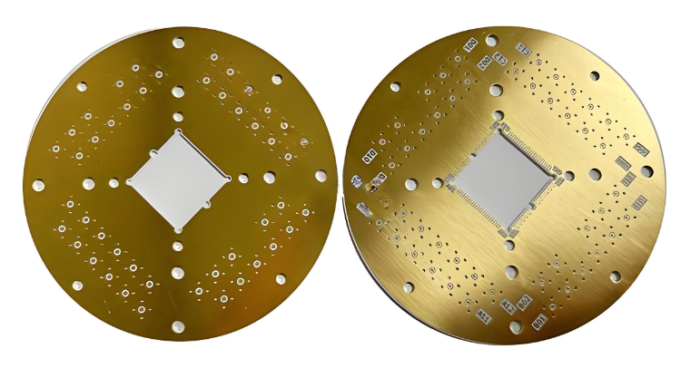
- Specialized Capabilities: Experts in advanced PCB types including Metal Core (MCPCB) for high-power applications, Ceramic PCBs, high-layer counts (up to 32 layers), and Heavy Copper PCBs (up to 20 oz).
- Speed to Market: We offer rapid prototyping with options for 24-hour shipping, crucial for iterative development and tight timelines. Our online WIP updates keep you informed.
- No MOQ Restrictions: We support projects of all scales, from initial prototype validation to full mass production, providing excellent flexibility for R&D teams and startups.
3. Commitment to Uncompromising Quality
Quality is embedded in our process. We hold ISO 9001, IATF 16949, and RoHS certifications, and our state-of-the-art facilities are equipped with rigorous testing protocols (AOI, X-Ray, Flying Probe Testing). This results in a high on-time delivery rate of 97% and products you can rely on.
4. Dedicated Support and Competitive Value
We believe in building partnerships. You will have a dedicated engineering sales contact for clear, responsive communication. By optimizing our production processes, we provide high-quality solutions at competitive prices, ensuring excellent return on your investment.
5. Proven Global Partner, Local Understanding
With over 1,700 satisfied clients across 40+ countries, including successful projects in South Africa, we have the experience to navigate local requirements and ensure a smooth, reliable supply chain for your projects.
In a nutshell, PCB manufacturing Cape Town represents a vital, responsive nerve center for South Africa’s electronics innovation, providing the speed and collaboration essential for modern product development. This guide has explored how local manufacturing benefits projects, compares regional hubs, and outlines what to look for in a top-tier printed circuit board partner.
EBest Circuit (Best Technology) has vast experience delivering innovative and practical solutions for PCB manufacturing South Africa projects. Our dedicated team supports customers in this region with reliable engineering and production services. For a quick quote or to download our full capabilities brochure, please feel free to contact us through the contact form at the bottom of our Contact Us Page.
FAQs
Q: How is a PCB manufactured?
A: The core PCB manufacturing process involves several key steps: designing the circuit layout, printing the pattern onto a laminate panel, etching away unwanted copper, drilling holes for components and vias, applying a solder mask and silkscreen, and finally performing electrical testing and quality inspection.
Q: How to start a PCB manufacturing business?
A: Starting a PCB manufacturing business requires significant capital investment in specialized PCB manufacturing machinery, deep technical expertise in chemical and electrical processes, obtaining relevant quality certifications, and developing a robust sales and supply chain network. It is a complex, capital-intensive venture.
Q: Is PCB manufacturing profitable?
A: PCB manufacturing can be profitable, but it operates on thin margins in high-volume, standard product segments. Profitability is higher in niche markets requiring advanced PCB manufacturing capabilities, such as prototyping, aerospace, medical, or specialized RF applications, where technical expertise adds significant value.