LED Backlight Module Aluminum PCB is a specialized printed circuit board designed to efficiently dissipate heat generated by LED backlight units in TVs and monitors, ensuring stable performance and extended lifespan. This blog will explore what this PCB is, its benefits, material composition, applications, selection tips, and more, while also offering solutions to common pain points faced by industry professionals.
Have you been struggling with these common issues?
- Frequent LED burnout due to poor heat dissipation in backlight modules
- Bulky, heavy cooling systems that increase product weight and design complexity
- Inconsistent performance across batches of PCBs for LED backlight modules
- High production costs from using inefficient thermal management solutions
- Difficulty finding custom aluminum PCB for LED backlight module that fit unique design specs
At EBest Circuit (Best Technology), we understand these challenges deeply. As a leading manufacturer specializing in high-performance PCBs, we’ve developed targeted solutions to resolve each of these pain points:
- Deploy high thermal conductivity aluminum PCB for LED backlight module to reduce LED operating temperatures by up to 30%
- Integrate slim, lightweight aluminum core designs to cut product weight by 25% while maintaining superior heat transfer
- Implement strict quality control processes to ensure 99.8% batch consistency for LED backlight aluminum module PCB
- Optimize material sourcing and production efficiency to lower overall costs by 15% without compromising quality
- Offer end-to-end custom aluminum PCB for LED backlight module services, from design consultation to prototype production
EBest Circuit (Best Technology) is a trusted name in the PCB manufacturing industry, with 20 years of experience producing high-quality, thermal-efficient circuit boards. We specialize in custom solutions for LED applications, leveraging advanced production facilities and a team of engineering experts to deliver products that meet the most stringent industry standards. Our state-of-the-art factory in China is equipped to handle both small-batch prototypes and large-scale production runs, ensuring on-time delivery and consistent quality. For inquiries about our LED backlight module aluminum PCB solutions, pls feel free to reach out to us at sales@bestpcbs.com.
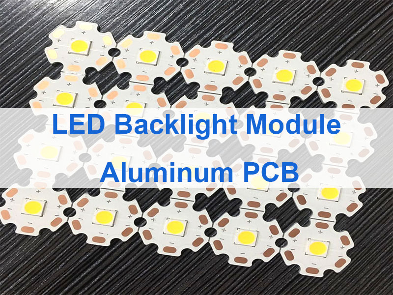
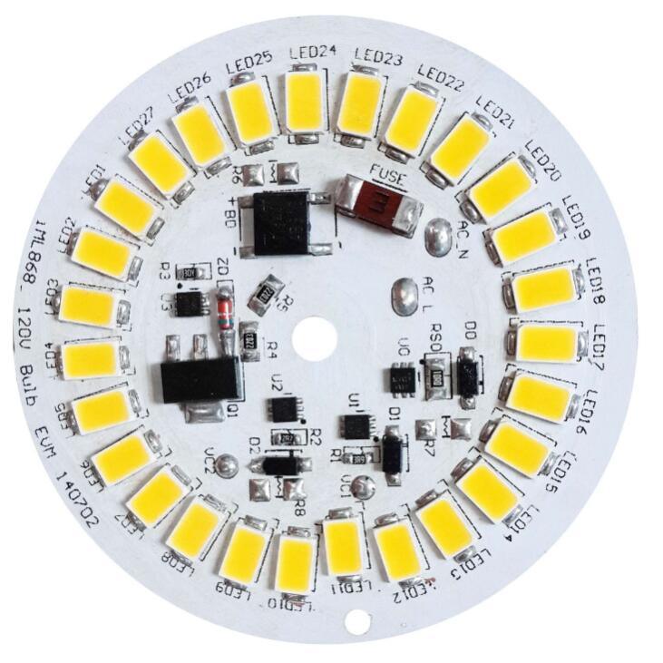
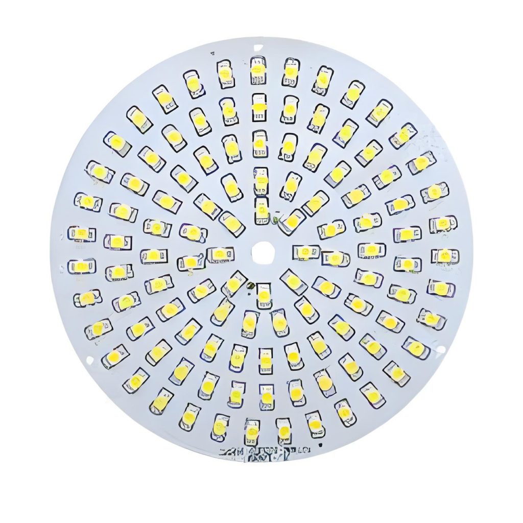
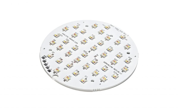
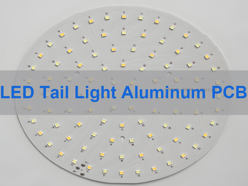
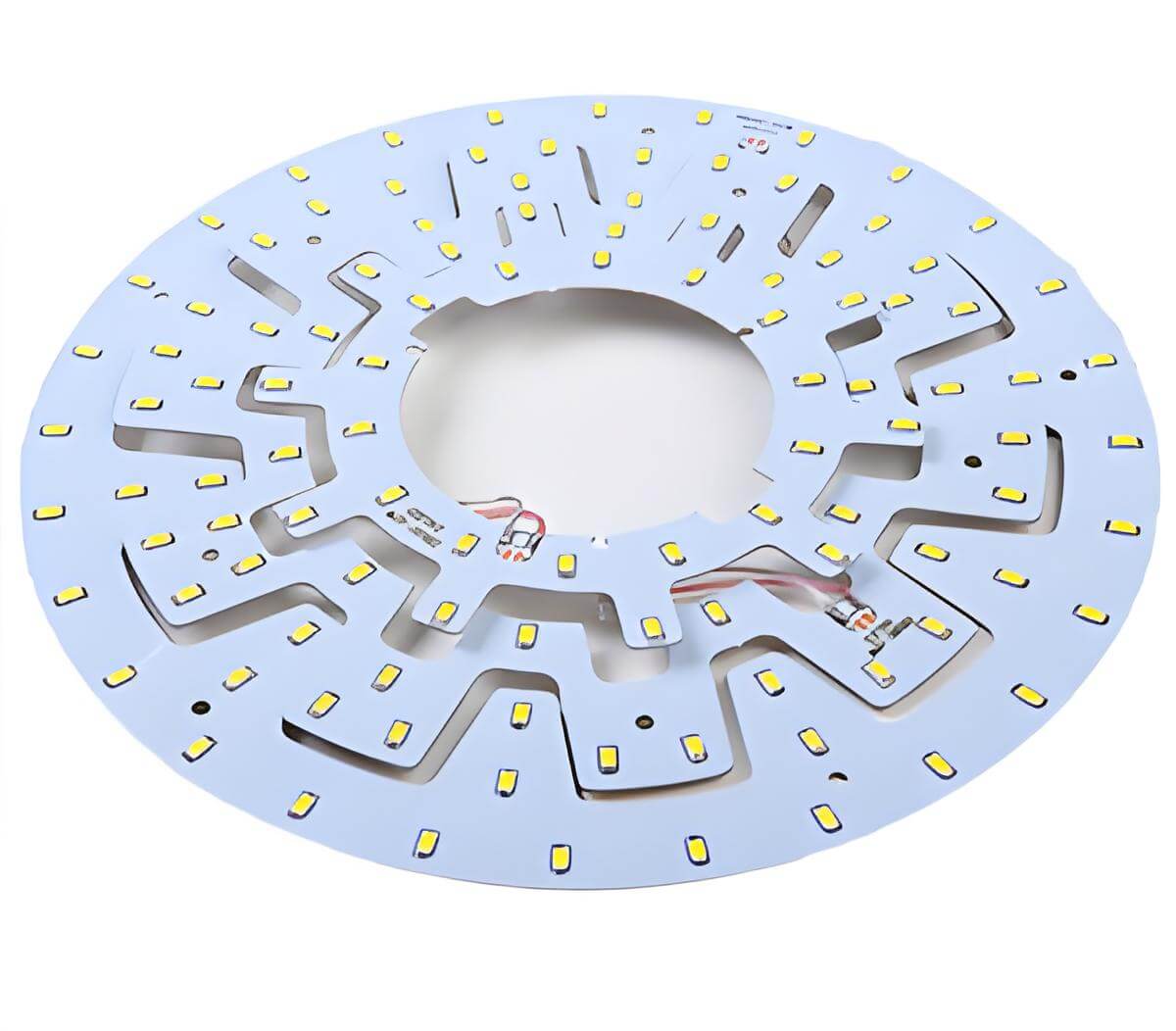
What Is an Aluminum PCB for LED Backlight Module?
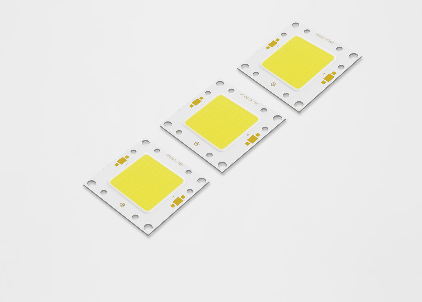
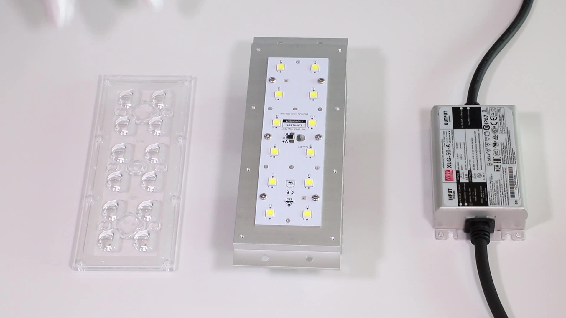
An Aluminum PCB for LED Backlight Module is a type of metal core printed circuit board that uses aluminum as the base material instead of traditional fiberglass. It is engineered to efficiently transfer heat away from LED components in TV and monitor backlight systems, preventing overheating and ensuring stable operation.
Key Characteristics:
- Aluminum core substrate for enhanced thermal conductivity
- Thin dielectric layer to facilitate rapid heat transfer
- Copper circuit layer optimized for LED current distribution
- Lightweight yet durable construction
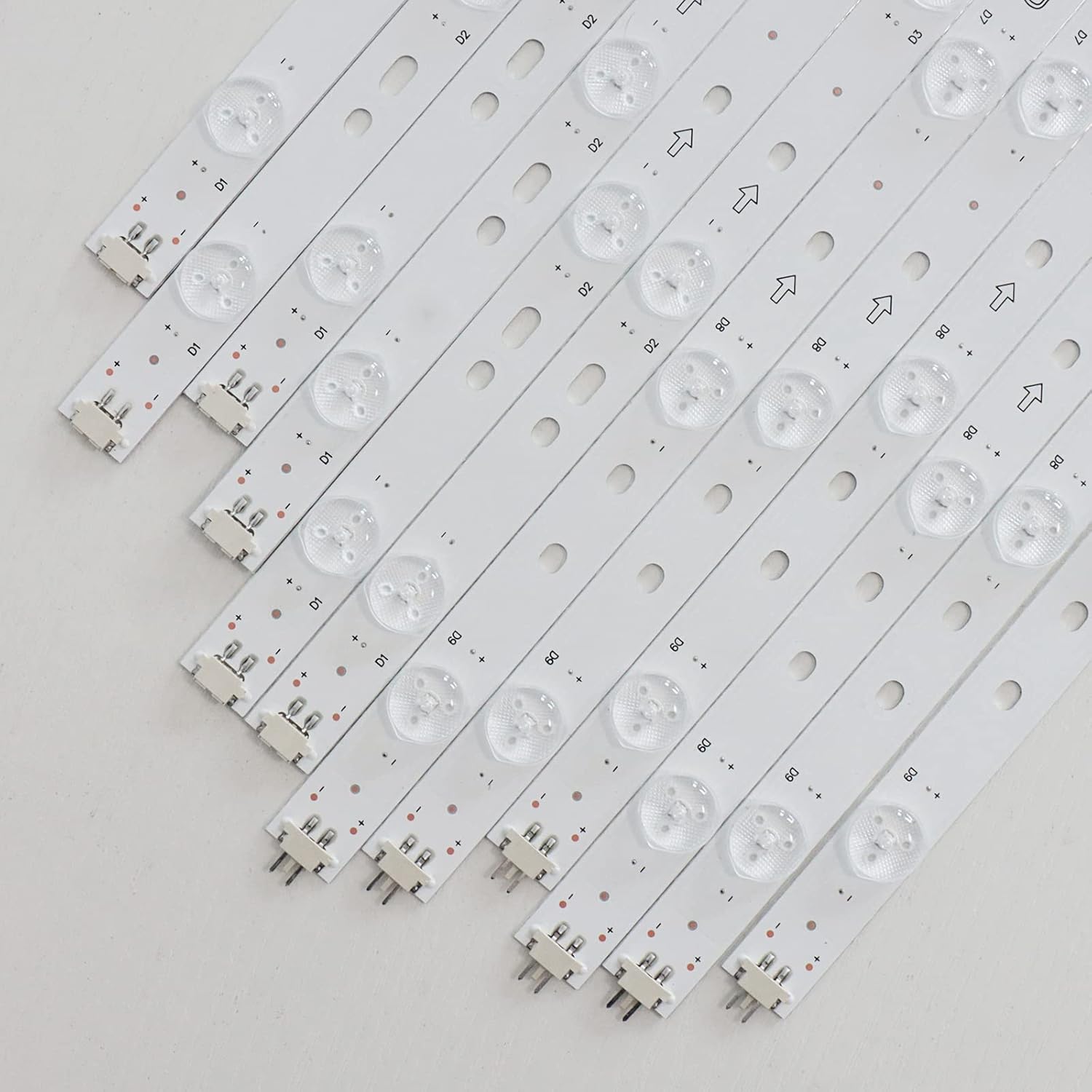
- Compatible with surface-mount device (SMD) LED components
In summary, this specialized PCB acts as a critical thermal management component, addressing the core issue of overheating in modern LED backlight systems.
Why Use Aluminum PCB for LED Backlight Module Design?
Choosing an Aluminum PCB for LED Backlight Module design offers significant advantages over traditional FR-4 PCBs, especially in high-power LED applications.
Core Benefits:
- Superior Heat Dissipation: Aluminum’s thermal conductivity is 10-20 times higher than FR-4, effectively reducing LED junction temperatures
- Extended LED Lifespan: Lower operating temperatures can increase LED lifespan by up to 50%
- Slimmer Design: Eliminates the need for bulky heat sinks, enabling thinner TV and monitor designs
- Improved Reliability: Reduces thermal stress on components, minimizing failure rates
- Cost Efficiency: Lower long-term maintenance and replacement costs due to enhanced durability
Overall, aluminum PCBs are the optimal choice for LED backlight module design, directly addressing the overheating challenges highlighted in our title.
How Does a PCB for LED Backlight Module Improve Heat Dissipation?
The heat dissipation mechanism of a PCB for LED Backlight Module relies on its layered structure and material properties to efficiently transfer heat away from LED components.
Heat Transfer Process:
- Heat Generation: LEDs produce heat during operation, which accumulates at the junction
- Conduction: Heat moves from the LED through the solder joint to the copper circuit layer
- Dielectric Layer Transfer: Thin, thermally conductive dielectric material transfers heat from the copper layer to the aluminum core
- Aluminum Core Distribution: The aluminum base spreads the heat across a larger surface area
- Convection/Radiation: Heat is released into the surrounding environment through natural convection or radiation
Efficiency Data:
| PCB Type | Thermal Conductivity (W/mK) | Typical LED Temperature Reduction |
|---|---|---|
| FR-4 PCB | 0.3-0.8 | 5-10°C |
| Aluminum PCB | 1-5 | 20-30°C |
| High-Performance Aluminum PCB | 5-10 | 30-40°C |
In conclusion, the layered structure and material selection of aluminum PCBs create an efficient heat dissipation pathway that directly solves the overheating problem in TV and monitor backlight modules.
EBest Circuit (Best Technology) is a professional metal core PCB manufacturer of LED Backlight Module Aluminum PCBs, offering reliable solutions with strong expertise in thermal management, structural design, and custom production. Pls feel free to contact us at +86-755-2909-1601 to discuss your project requirements.
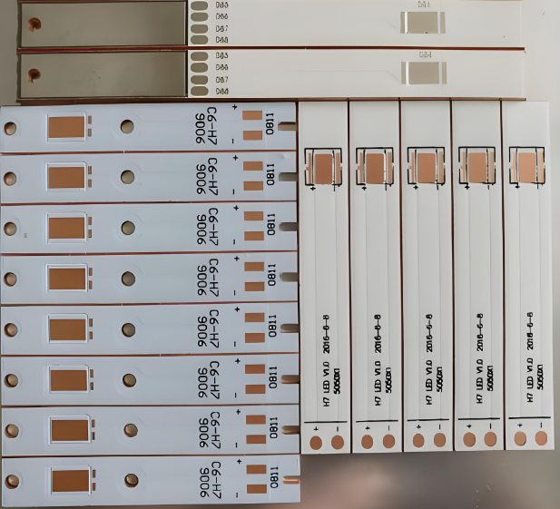
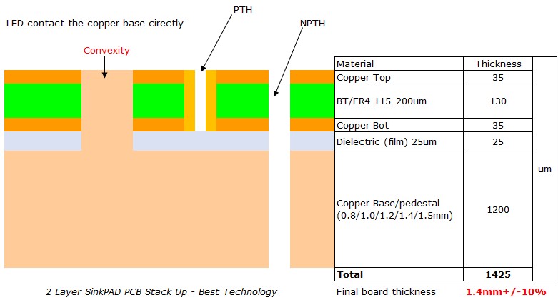
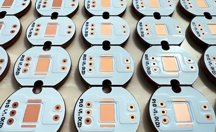
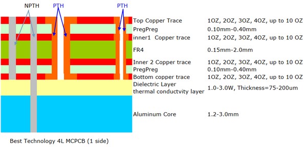
What Materials Are Used in LED Backlight Module Aluminum PCB?
LED Backlight Module Aluminum PCB consists of three main layers, each using specialized materials to balance thermal performance, electrical insulation, and mechanical strength.
Layer Composition:
- Aluminum Base Layer:
- Material: 1060, 6061, or 5052 aluminum alloy
- Purpose: Provides structural support and heat spreading
- Thermal Conductivity: 160-200 W/mK
- Dielectric Layer:
- Material: Thermally conductive epoxy resin or ceramic-filled polymer
- Purpose: Electrically insulates the circuit layer from the aluminum base while transferring heat
- Thermal Conductivity: 1-10 W/mK
- Copper Circuit Layer:
- Material: Electrodeposited or rolled copper
- Purpose: Forms the electrical circuit for LED power distribution
- Thickness: 1oz-3oz (35μm-105μm)
Material Selection Guide:
| Application | Recommended Aluminum Alloy | Dielectric Type | Copper Thickness |
|---|---|---|---|
| Small Monitors | 1060 | Standard epoxy | 1oz |
| Large Smart TVs | 6061 | High-performance ceramic-filled | 2oz |
| Industrial Displays | 5052 | High-temperature epoxy | 3oz |
To summarize, the combination of aluminum alloy, thermally conductive dielectric, and copper creates a PCB that excels in thermal management for LED backlight modules.
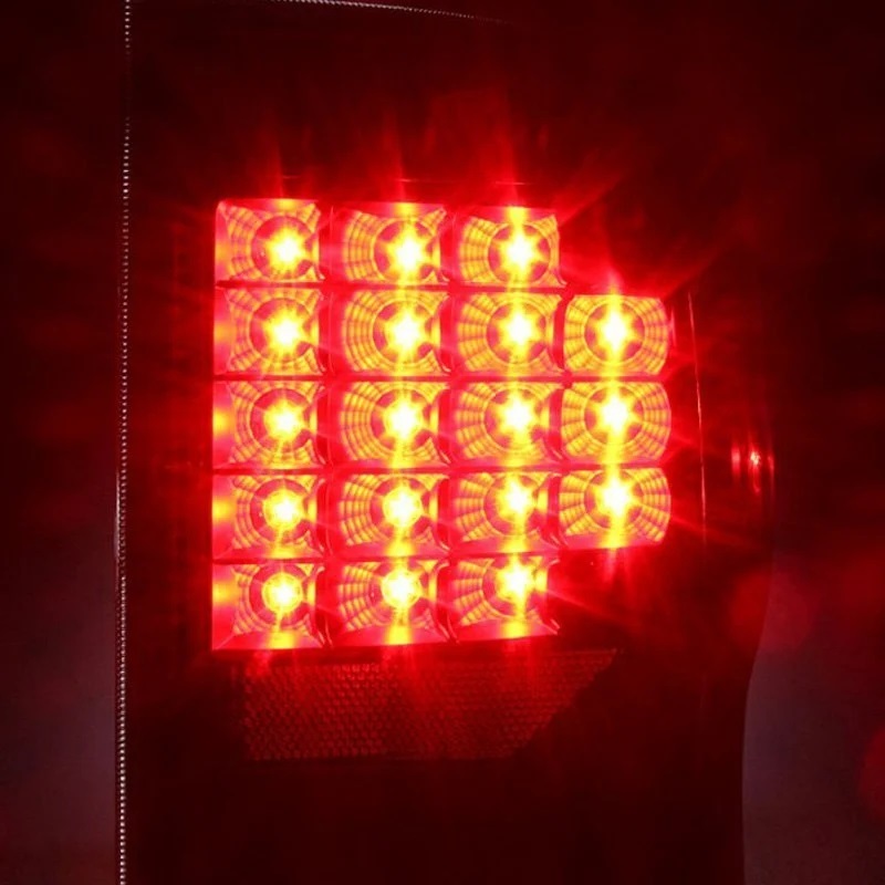
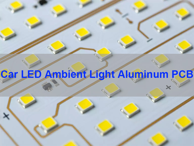
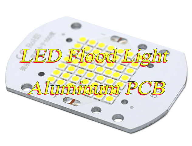
Where Are Aluminum PCBs for LED Backlight Modules Used?
Aluminum PCBs for LED Backlight Modules are essential components in a wide range of display devices, where efficient heat dissipation is critical for performance and longevity.
Key Applications:
- Smart TVs: From 32-inch budget models to 8K ultra-large screens
- Computer Monitors: Including gaming monitors, professional displays, and all-in-one PCs
- Digital Signage: Large outdoor displays and indoor advertising screens
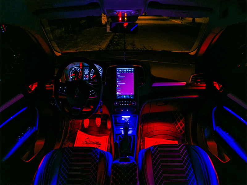
- Automotive Displays: In-car infotainment systems and instrument clusters
- Industrial Displays: Rugged monitors for manufacturing and control rooms
Market Growth Data:
- Global LED backlight PCB market is projected to reach $4.2 billion by 2028
- Automotive display applications are growing at a CAGR of 8.5%
- Demand for high thermal conductivity aluminum PCB for LED backlight module is increasing with the adoption of mini-LED and micro-LED technologies
In short, wherever there’s an LED backlight system in need of reliable thermal management, aluminum PCBs play a vital role.
How to Choose the Right Aluminum PCB for Backlight Module Applications?
Selecting the right Aluminum PCB for Backlight Module applications requires careful consideration of several key factors to ensure optimal performance and cost-effectiveness.
Selection Criteria:
- Thermal Requirements: Calculate the total heat output of your LED array and choose a PCB with sufficient thermal conductivity
- Aluminum Alloy Type: 1060 for general use, 6061 for higher strength, 5052 for corrosion resistance
- Dielectric Layer Performance: Match dielectric thermal conductivity to your heat dissipation needs
- Copper Thickness: 1oz for low-power LEDs, 2-3oz for high-density backlight modules
- Customization Options: Ensure the manufacturer can provide custom aluminum PCB for LED backlight module with specific shapes and sizes
- Quality Certifications: Look for IPC-A-600, ISO 9001, and RoHS compliance
- Cost vs. Performance: Balance thermal performance requirements with budget constraints
Quick Selection Checklist:
- [ ] Calculate LED power consumption and heat output
- [ ] Determine required thermal conductivity
- [ ] Select appropriate aluminum alloy and dielectric material
- [ ] Choose copper thickness based on current requirements
- [ ] Verify manufacturer’s customization capabilities
- [ ] Check for relevant industry certifications
By following these guidelines, you can confidently select the best aluminum PCB for your specific backlight module application.
What Are the Benefits of Custom PCB for LED Backlight Module Projects?
Opting for a custom PCB for LED backlight module projects offers significant advantages over off-the-shelf solutions, especially for specialized or high-volume applications.
Advantages of Customization:
- Tailored Thermal Performance: Design the PCB layout and material specifications to match your exact heat dissipation needs
- Space Optimization: Create unique shapes and sizes to fit compact or irregular backlight module designs
- Cost Reduction: Eliminate unnecessary features and optimize material usage to lower production costs
- Improved Reliability: Custom layouts can reduce trace resistance and improve current distribution, enhancing overall system stability
- Faster Time-to-Market: Partner with a manufacturer that offers end-to-end custom services to streamline the design and production process
- Scalability: Develop a custom solution that can be easily scaled from prototype to mass production
- Competitive Edge: Differentiate your products with unique features and performance characteristics
Customization Process at EBest Circuit:
- Design Consultation: Our engineers work with you to understand your requirements and propose optimal solutions
- Prototype Development: We create a small batch of prototypes for testing and validation
- Design Optimization: Based on test results, we refine the design for optimal performance
- Mass Production: Once the design is finalized, we handle large-scale production with strict quality control
- Delivery and Support: We ensure on-time delivery and provide ongoing technical support
In summary, custom PCBs enable you to create LED backlight modules that perfectly meet your specific design requirements, performance goals, and budget constraints.
All in all, LED Backlight Module Aluminum PCB is a specialized thermal management solution that effectively addresses the overheating challenges in TV and monitor backlight systems, ensuring stable performance and extended component lifespan. This blog has covered everything from the basics of what this PCB is to advanced topics like material selection, customization benefits, and application scenarios, while also providing practical solutions to common industry pain points.
At EBest Circuit (Best Technology), we pride ourselves on delivering high-quality, custom aluminum PCB solutions for LED backlight module applications. With our advanced production capabilities, engineering expertise, and commitment to quality, we can help you create display products that stand out in the market. For more information about our services or to request a quote, please contact us at sales@bestpcbs.com.
FAQ About Aluminum PCB for LED Backlight Module
Q: What is the typical lifespan of an Aluminum PCB for LED Backlight Module?
A: With proper design and usage, aluminum PCBs can last 10-15 years, matching the lifespan of most LED backlight systems.
Q: Can Aluminum PCBs be used for outdoor LED displays?
A: Yes, with proper corrosion-resistant coating and material selection (such as 5052 aluminum alloy), aluminum PCBs are suitable for outdoor applications.
Q: How does the cost of an Aluminum PCB compare to a traditional FR-4 PCB?
A: Aluminum PCBs typically cost 2-3 times more than FR-4 PCBs, but the long-term savings from reduced maintenance and extended LED lifespan often offset the initial investment.
Q: Can I get a custom aluminum PCB for LED backlight module with unique shapes?
A: Yes, most specialized PCB manufacturers, including EBest Circuit, offer custom cutting and shaping services to meet unique design requirements.
Q: What is the maximum size of an Aluminum PCB for LED Backlight Module that can be produced?
A: At EBest Circuit, we can produce aluminum PCBs up to 1200mm x 600mm, suitable for large-format TV and monitor backlight modules.
Q: How long does it take to produce a custom aluminum PCB for LED backlight module?
A: The production time varies depending on complexity and order size, but typically ranges from 7-14 days for prototypes and 15-25 days for mass production.