Medical Equipment PCB serves as the central nervous system of modern healthcare technology, enabling everything from portable monitors to advanced imaging systems to function with precision and reliability. This article explores the critical aspects of selecting and working with medical PCB suppliers who can deliver both quality and speed, ensuring your medical devices meet the highest standards while reaching the market faster.
Many medical device companies face significant challenges when sourcing PCBs. Have you encountered these issues in your projects?
- Stringent Compliance Requirements: Navigating complex medical regulations (FDA, ISO 13485, IEC 60601) without expert guidance
- Unreliable Delivery Timelines: Production delays due to PCB suppliers missing critical deadlines
- Quality Consistency Issues: Inconsistent PCB performance affecting device reliability and patient safety
- Limited Technical Expertise: Suppliers lacking specialized knowledge in medical-grade PCB design and manufacturing
- Scalability Challenges: Difficulty transitioning from prototypes to full-scale production without compromising quality
Fortunately, these challenges can be effectively addressed through strategic partnership selection. The solution lies in:
- Comprehensive Certification Management: Partnering with suppliers who maintain up-to-date medical industry certifications and understand compliance documentation
- Guaranteed Rapid Delivery: Selecting manufacturers with proven track records of on-time delivery, even for complex multilayer boards
- Rigorous Quality Processes: Implementing thorough testing protocols (AOI, flying probe, impedance testing) throughout production
- Medical-Specific Design Support: Accessing engineering expertise specialized in medical device requirements and constraints
- Seamless Scaling Capabilities: Working with suppliers who offer smooth transitions from prototyping to volume manufacturing
At BEST Technology, we specialize in addressing these critical needs through our expertise in medical-grade PCB manufacturing and commitment to rapid delivery. Our certified manufacturing facilities and medical industry experience make us the ideal partner for your healthcare technology projects. Pls feel free to contact us at sales@bestpcbs.com to discuss your specific requirements.

What Is a Medical Equipment PCB?
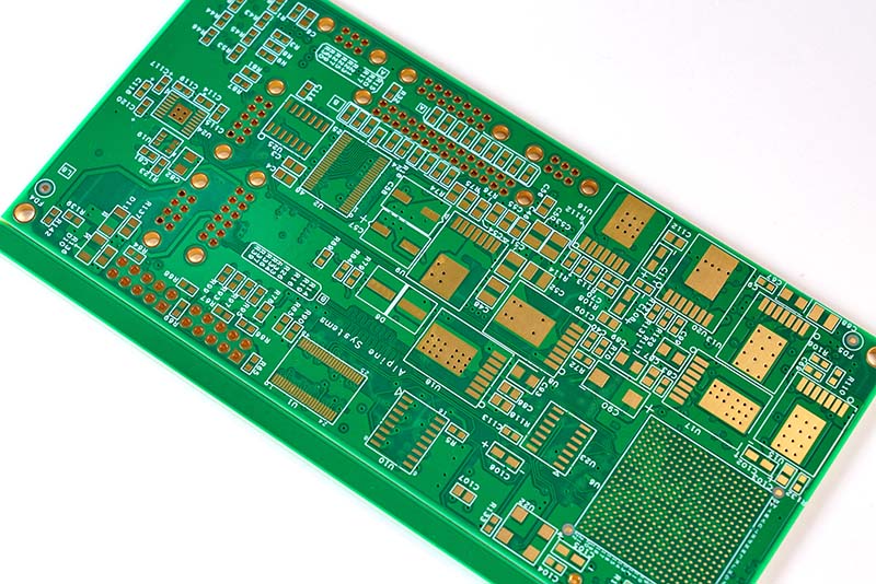
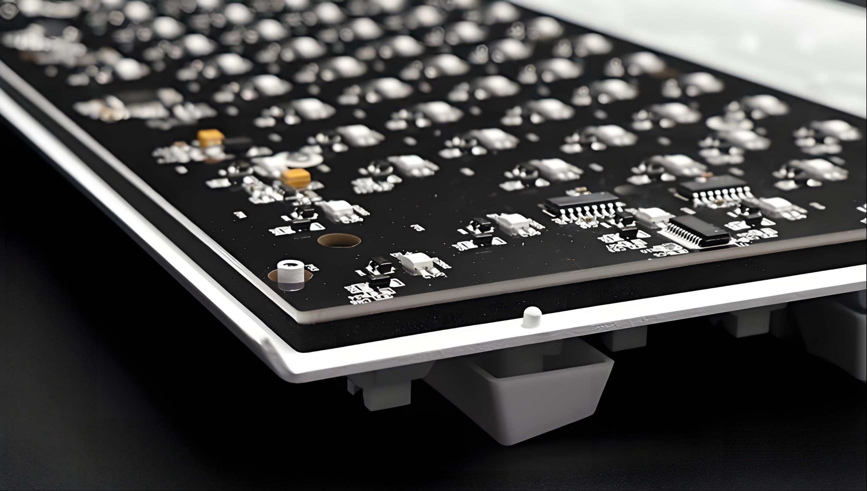
Medical Equipment PCB forms the fundamental infrastructure that enables electronic medical devices to function reliably, often in life-critical applications. Unlike standard circuit boards, medical PCBs must meet exceptionally high standards for reliability, precision, and safety since they directly impact patient diagnosis, treatment, and monitoring outcomes. These specialized printed circuit boards serve as the central nervous system of medical devices, ensuring accurate signal processing, power distribution, and data communication in everything from portable glucose monitors to advanced MRI machines .
The distinction between medical PCBs and conventional circuit boards becomes apparent when examining three key areas: regulatory compliance, material selection, and performance requirements. Medical PCBs must comply with international standards such as ISO 13485 for quality management systems and IEC 60601-1 for electrical safety of medical equipment. They often require biocompatible materials when there’s potential for patient contact, and must demonstrate exceptional reliability with mean time between failures (MTBF) rates significantly higher than commercial-grade boards .
Key Applications in Medical Devices
- Diagnostic Equipment: PCBs used in imaging systems like CT scanners, ultrasound machines, and X-ray equipment require high-frequency capabilities and precise signal integrity to ensure accurate image reconstruction and diagnosis .
- Patient Monitoring Devices: Boards for vital signs monitors, ECG machines, and pulse oximeters demand stable performance and low noise levels to accurately track patient health metrics without interference .
- Therapeutic Devices: PCBs in infusion pumps, surgical lasers, and neurostimulators must offer fail-safe operation and redundant safety features to prevent patient harm during treatment .
- Portable and Wearable Medical Devices: These applications require compact, lightweight, and often flexible PCB designs that can withstand movement while maintaining reliable connectivity .
- Laboratory Automation: Medical PCBs in automated analyzers and laboratory equipment need robust communication interfaces and precision timing to handle complex testing procedures .
Table: Medical vs. Commercial PCB Requirements
| Characteristic | Medical PCBs | Commercial PCBs |
|---|---|---|
| Quality Standards | ISO 13485, ISO 9001, IEC 60601-1 | ISO 9001, basic IPC standards |
| Lifespan Expectation | 10+ years with high reliability | 3-5 years with acceptable failure rates |
| Testing Requirements | Extensive testing (environmental, electrical, biocompatibility) | Basic functional testing |
| Traceability | Full material and process traceability | Limited batch tracing |
| Cleanliness Standards | Certified cleanroom assembly (Class 1000 or better) | Standard manufacturing environment |
Medical equipment PCBs represent a specialized category where failure is not an option. The stringent requirements governing their design, materials, and manufacturing processes directly correlate with their intended use in preserving human health and lives. Understanding these fundamental distinctions helps medical device manufacturers make informed decisions when selecting PCB partners for their critical healthcare applications .

What Design Factors Ensure High Reliability in a BGA PCB Board for Medical Equipment?
BGA PCB Board for Medical Equipment demands exceptional reliability since these components often serve in life-critical applications where failure could compromise patient safety. The Ball Grid Array packaging technology, with its high pin count and small footprint, presents both opportunities and challenges for medical device designers who must balance performance with absolute reliability .
The miniaturization benefits of BGA packages come with specific design considerations that directly impact medical device reliability. Unlike traditional components with perimeter leads, BGAs utilize an array of solder balls underneath the component, creating challenges for inspection, thermal management, and mechanical stress distribution. For medical applications, where devices may undergo rigorous daily use or serve in implantable applications, each of these factors requires careful consideration during the design phase .
Critical Design Elements for Medical BGA Reliability
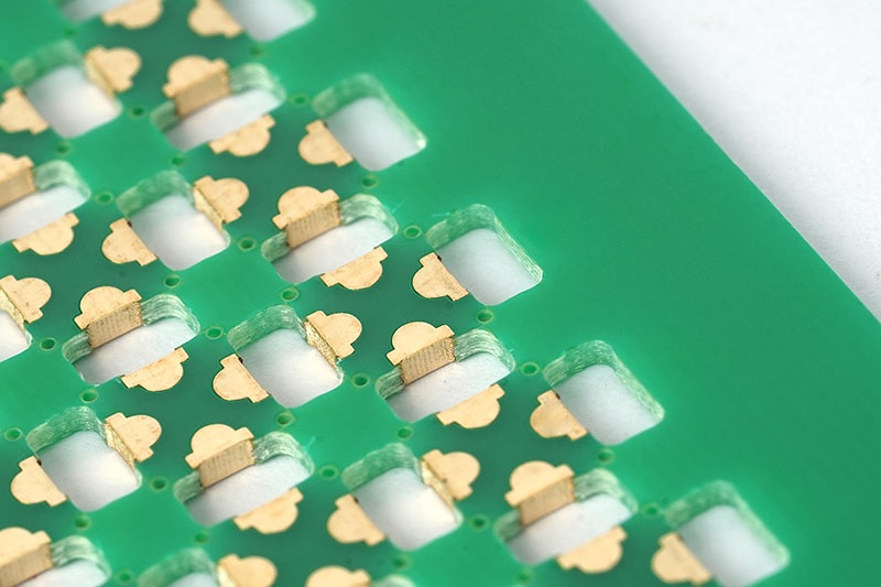
- Thermal Management Strategies: Medical devices often operate continuously, generating heat that must be effectively dissipated. Implement thermal vias directly under BGA packages to transfer heat to internal ground planes or heat spreaders, preventing overheating that could compromise solder joint integrity .
- Pad Size and Solder Mask Definition: Precisely controlled pad sizes and solder mask openings ensure proper solder ball formation during reflow. For medical devices, we recommend slightly larger solder mask openings (0.1mm oversize) to create robust solder joints while preventing solder bridging between fine-pitch BGA pads .
- Structured Design Rules: Implement conservative trace width and spacing rules specific to medical BGA designs. For BGAs with pitch below 0.8mm, use 0.075mm trace width with 0.075mm spacing to maintain signal integrity while accommodating manufacturing tolerances .
- Dielectric Material Selection: Choose PCB substrates with matched coefficient of thermal expansion (CTE) to the BGA component. This prevents thermal cycling stress that can crack solder joints in medical devices subjected to repeated sterilization cycles or environmental variations .
- Via-in-Pad and Microvia Technology: Utilize filled and capped via-in-pad designs for high-density BGAs to escape signals efficiently while maintaining a flat surface for ball attachment. Stacked microvias beneath medical BGAs enhance reliability by providing shorter electrical paths and better thermal characteristics.
- Signal Integrity Considerations: Medical devices require pristine signal quality for accurate data acquisition. Implement impedance-controlled routing, ground shielding, and length matching for critical signals emanating from BGAs, particularly in analog front-end circuits for patient monitoring .
- Test Access Points: Incorporate test points for critical nets when possible, even if they require specialized fixtures. Medical device validation demands comprehensive testing, and accessible test points facilitate in-circuit testing and field diagnostics .
Table: BGA Reliability Design Rules for Medical Applications
| BGA Pitch | Recommended Pad Diameter | Via Size | Escape Routing Strategy |
|---|---|---|---|
| 1.0mm | 0.5mm | 0.3mm (mechanical) | Dog-bone fanout with 2 signal rows between pads |
| 0.8mm | 0.4mm | 0.2mm (laser) | Direct via-in-pad with 1 signal row between pads |
| 0.5mm | 0.25mm | 0.1mm (laser) | Microvia-in-pad with HDI buildup layers |
| 0.4mm and below | 0.22mm | 0.075mm (laser) | Advanced HDI with any-layer microvia technology |
The reliability of BGA assemblies in medical equipment ultimately depends on a holistic approach that considers the entire ecosystem—from material selection and thermal design to manufacturing processes and testing protocols. By addressing these factors during the design phase, medical device manufacturers can leverage the performance benefits of BGA technology while meeting the stringent reliability requirements essential for healthcare applications .
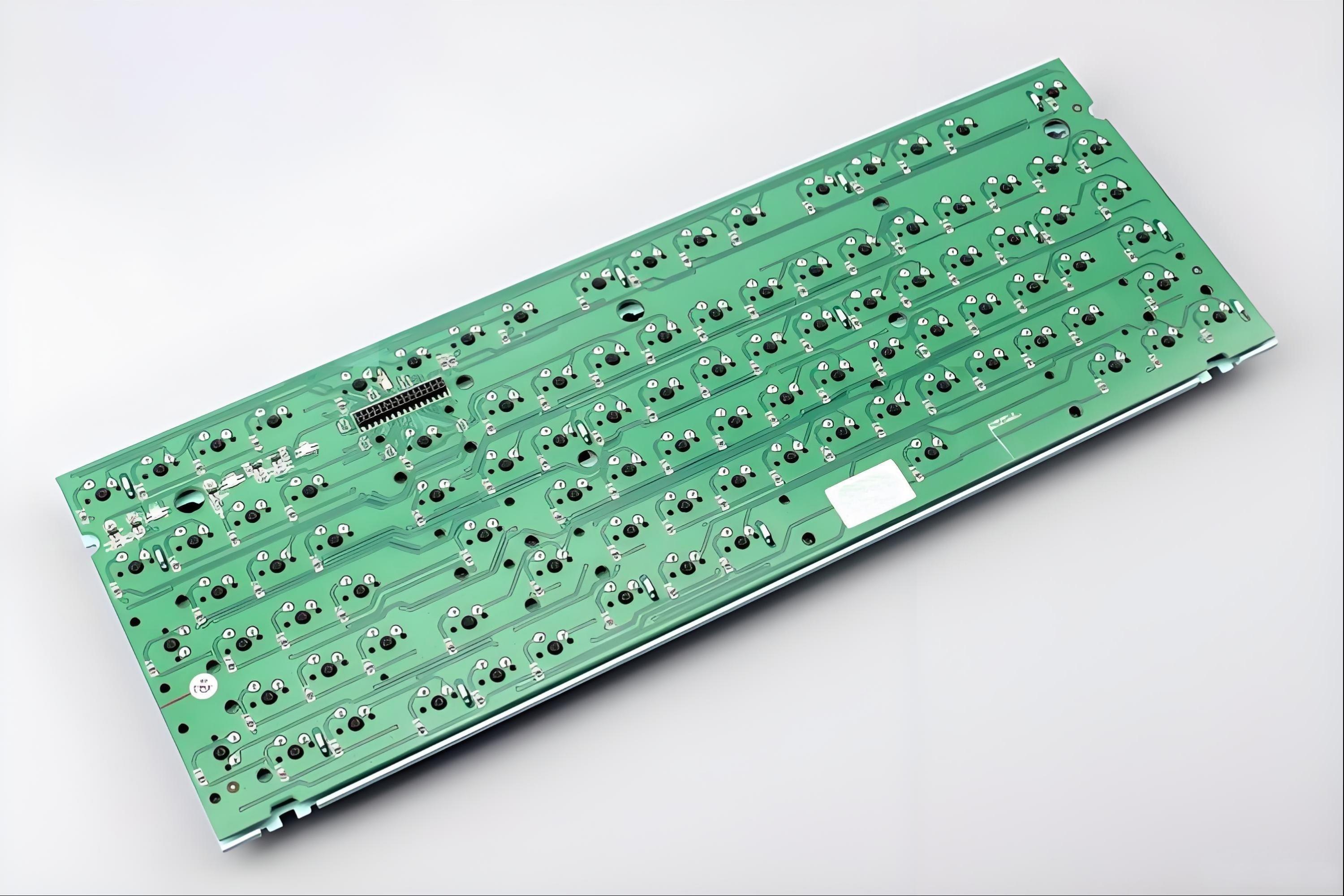
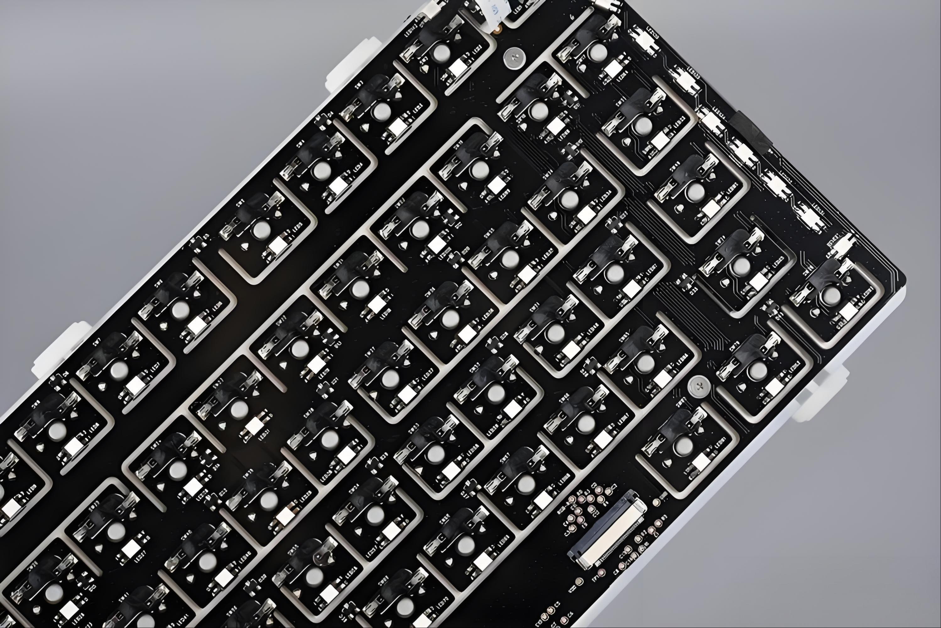
Why Do Portable Devices Depend on the Best Rigid-Flex PCB Suppliers for Portable Medical Equipment?
Best Rigid-Flex PCB Suppliers for Portable Medical Equipment play a critical role in overcoming the unique challenges of medical device miniaturization, durability, and performance. Portable medical devices—including wearable monitors, handheld diagnostic tools, and implantable devices—demand circuit boards that can withstand bending, vibration, and repeated use while maintaining reliable operation in life-critical applications .
The structural advantages of rigid-flex PCBs make them particularly suitable for portable medical equipment where space constraints, weight reduction, and reliability are paramount. By integrating both rigid and flexible circuit sections into a single interconnected structure, rigid-flex technology eliminates the need for connectors and cabling that traditionally represent points of failure in portable devices. This consolidation creates more robust medical devices capable of surviving the mechanical stresses inherent in portable healthcare applications .
Key Benefits of Rigid-Flex Technology in Medical Devices
- Space Optimization and Weight Reduction: Medical rigid-flex boards can be precisely folded into 3D configurations that conform to available space within compact medical device housings, achieving up to 60% space savings compared to traditional rigid boards with connectors. This enables more compact, lightweight, and patient-friendly portable medical devices .
- Enhanced Reliability and Durability: By eliminating connection points between multiple boards, rigid-flex constructions reduce failure points by up to 70%, significantly improving mean time between failures (MTBF). This is particularly critical for medical devices subjected to regular movement, sterilization cycles, or implantable applications where reliability directly impacts patient safety .
- Improved Signal Integrity: Continuous impedance-controlled traces running between rigid sections maintain signal quality in sensitive medical monitoring applications. High-speed digital signals and low-level analog signals are protected from interference that could compromise diagnostic accuracy in devices like ECG monitors and neural recorders .
- Streamlined Assembly Processes: Integrated rigid-flex constructions reduce component count and simplify final assembly, resulting in more automated manufacturing with fewer manual steps. This enhances quality consistency while reducing manufacturing costs for volume production of portable medical equipment .
- Thermal Management Capabilities: Flexible sections can help dissipate heat away from sensitive components more effectively than traditional designs. This thermal management benefit is crucial for battery-powered portable medical devices where heat buildup could affect performance or patient comfort during extended use .
- Design Flexibility for Ergonomic Devices: The ability to create unconventional form factors enables medical device designers to develop ergonomic products that fit naturally in clinical settings or on patient bodies. This human factors consideration is increasingly important in patient-centric healthcare technology design .
Table: Rigid-Flex PCB Selection Criteria for Medical Applications
| Design Consideration | Portable Medical Requirement | Supplier Capability Needed |
|---|---|---|
| Bend Cycles | 10,000+ for wearable devices | Dynamic flex rating with polyimide coverlay |
| Layer Count | 4-12 layers typical | Microvia capability (0.1mm) with sequential lamination |
| Impedance Control | ±10% tolerance for high-speed signals | Experience with mixed dielectric stackups |
| Medical Certifications | ISO 13485, ISO 10993 biocompatibility | Certified medical manufacturing facilities |
| Testing Protocols | 100% electrical testing with medical-grade AQL | Flying probe and custom fixture testing expertise |
Selecting the right rigid-flex PCB supplier requires careful evaluation of their medical industry experience, quality systems, and technical capabilities. The best suppliers offer comprehensive design support, regulatory compliance expertise, and proven reliability in producing boards that meet the stringent requirements of portable medical equipment. This partnership approach ensures that medical device manufacturers can leverage the full benefits of rigid-flex technology while meeting their time-to-market and regulatory objectives .
How Do OEM Medical Equipment PCB Factories Deliver Durable and High-Precision PCB Assemblies?
OEM Medical Equipment PCB Factories specialize in transforming design concepts into reliable, high-precision medical devices through comprehensive manufacturing capabilities, stringent quality controls, and medical-specific expertise. These original equipment manufacturer facilities serve as essential partners in the medical device ecosystem, providing the technological foundation upon which healthcare innovations are built .
The medical device manufacturing process at OEM PCB factories differs significantly from commercial PCB production through enhanced process controls, specialized documentation, and rigorous testing protocols. These facilities typically operate under ISO 13485 quality management systems specifically tailored for medical devices, implementing traceability measures that track every component and process parameter from raw materials to finished assemblies. This level of control ensures consistent performance and facilitates rapid root cause analysis should any field issues arise .
Key OEM Capabilities for Medical PCB Assemblies
- Advanced Manufacturing Technologies: Leading medical OEMs employ sophisticated equipment for high-precision assembly, including automated optical positioning systems that achieve placement accuracy of 25μm or better for fine-pitch components. Laser direct imaging (LDI) systems with 5μm resolution ensure precise pattern transfer for dense medical PCB designs requiring impedance control and signal integrity .
- Comprehensive Material Management: Medical OEMs maintain strict control over PCB materials, often utilizing medical-grade laminates with proven performance characteristics. For implantable devices, this includes biocompatible materials that meet ISO 10993 standards, while high-frequency applications may require specialized substrates with stable dielectric properties for accurate signal transmission in diagnostic equipment .
- Robust Quality Assurance Systems: Medical PCB factories implement multi-stage inspection regimes combining automated optical inspection (AOI), X-ray inspection for hidden joints (particularly important for BGA components), and electrical testing. These facilities typically maintain statistical process control (SPC) with Cpk values exceeding 1.67 for critical processes, ensuring predictable, high-yield production of medical devices .
- Cleanroom Manufacturing Environments: Depending on device classification, medical PCBs may be assembled in controlled environments ranging from Class 100,000 to Class 100 cleanrooms. This prevents contamination that could compromise device reliability or patient safety, particularly for implants or devices used in surgical environments .
- Specialized Process Expertise: Medical OEMs develop expertise with processes critical to healthcare applications, including thick copper processing for power sections, hybrid rigid-flex assembly for portable devices, and conformal coating applications that protect boards from fluids and contaminants encountered in medical settings .
- Comprehensive Testing and Validation: Beyond standard electrical testing, medical OEMs perform device-specific validation including burn-in testing, environmental stress screening, and functional testing that simulates actual use conditions. This ensures the finished PCB assembly will perform reliably in its intended medical application .
- Regulatory Documentation Support: Experienced medical OEMs provide comprehensive documentation packages including device history records, material certifications, and test reports that streamline regulatory submissions for FDA, CE marking, and other medical device approvals .
Table: Medical vs. Commercial PCB Assembly Requirements
| Parameter | Medical OEM Requirements | Commercial PCB Assembly |
|---|---|---|
| Quality Standards | ISO 13485, ISO 9001, IPC-A-610 Class 3 | ISO 9001, IPC-A-610 Class 2 |
| Traceability | Full component-level traceability with lot tracking | Basic batch tracking |
| Cleanroom Requirements | Class 100,000 to Class 100 depending on application | Standard factory environment |
| Acceptable Quality Level (AQL) | 0.1% for critical characteristics | 0.65% – 1.5% typical |
| Documentation | Comprehensive device history records | Basic compliance documentation |
The combination of technical capabilities, quality systems, and medical industry expertise enables OEM medical equipment PCB factories to deliver the durable, high-precision assemblies essential for healthcare applications. By partnering with experienced medical OEMs, device manufacturers can accelerate development timelines while ensuring their products meet the rigorous reliability and regulatory requirements of the global healthcare market .
Why Are China Medical Equipment PCB Manufacturers a Strong Choice for Scalable Production?
China Medical Equipment PCB Manufacturer capabilities have evolved to offer world-class production scalability combined with competitive pricing, making them an attractive option for medical device companies seeking to balance quality, volume, and cost considerations. The Chinese PCB industry has made significant investments in medical-grade manufacturing infrastructure, quality systems, and regulatory compliance expertise to meet the stringent requirements of healthcare applications .
The manufacturing ecosystem for medical PCBs in China benefits from extensive vertical integration, with suppliers often offering end-to-end services from PCB fabrication to component sourcing and final assembly. This comprehensive approach streamlines the supply chain for medical device companies, reducing coordination complexity while maintaining single-source accountability for quality and delivery. Many Chinese manufacturers have developed specialized medical divisions with dedicated cleanrooms, medical-grade testing equipment, and staff trained specifically in healthcare industry requirements .
Advantages of Chinese Medical PCB Manufacturers
- Scalable Production Capacity: Chinese PCB manufacturers typically operate large-scale facilities with significant excess capacity, enabling them to accommodate sudden volume increases or large production runs without compromising delivery timelines. This scalability is particularly valuable for medical devices that may experience unpredictable demand fluctuations based on healthcare market dynamics .
- Cost-Effective Manufacturing: The combination of advanced automation, vertical integration, and economies of scale allows Chinese manufacturers to offer competitive pricing while maintaining medical-grade quality. For volume production, cost savings of 30-50% compared to Western manufacturers are common without compromising on specifications or reliability .
- Comprehensive Medical Certifications: Leading Chinese PCB manufacturers have invested heavily in obtaining international medical certifications, with many facilities holding ISO 13485, ISO 9001, and compliance with IEC 60601-1 standards. These certifications demonstrate adherence to the same rigorous quality management systems required of medical device manufacturers worldwide .
- Technical Expertise and Innovation: Contrary to outdated perceptions, many Chinese PCB manufacturers employ advanced engineering capabilities including HDI technology, impedance control, and rigid-flex expertise specifically tailored for medical applications. Regular collaboration with international medical companies has accelerated knowledge transfer and quality improvement initiatives .
- Supply Chain Resilience and Flexibility: The concentrated electronics manufacturing ecosystem in China provides robust supply chain options for medical PCB materials and components. This density creates resilience against disruptions and offers flexibility for design changes or material substitutions when necessary .
- Rapid Prototyping and Tooling: Chinese manufacturers have perfected rapid turnaround processes, with many offering 24-48 hour prototype services that accelerate medical device development cycles. This speed-to-market advantage is particularly valuable during iterative design phases and clinical validation stages .
Table: Comparison of Medical PCB Manufacturing Regions
| Capability | Chinese Manufacturers | North American/European Manufacturers |
|---|---|---|
| Production Volume Scalability | High (large facility capacity) | Medium (typically smaller facilities) |
| Cost Structure | Competitive (30-50% lower) | Higher (premium pricing) |
| Regulatory Compliance | ISO 13485, IEC 60601-1 common | ISO 13485, IEC 60601-1 standard |
| Lead Time Flexibility | 24-48 hour prototypes common | 5-10 day prototypes typical |
| IP Protection Framework | Improving with specialized contracts | Established legal frameworks |
While Chinese medical PCB manufacturers offer compelling advantages for scalable production, device manufacturers should conduct thorough due diligence focusing on quality systems, regulatory compliance history, and specific medical industry experience. The most successful partnerships often involve clear communication protocols, regular quality audits, and well-defined specifications that align international quality expectations with Chinese manufacturing capabilities .
How Does a Fast PCB Prototype Assembly Supplier for Medical Devices and Equipment Accelerate Development?
Fast PCB Prototype Assembly Supplier for Medical Devices and Equipment plays a critical role in compressing development timelines while ensuring design validation through rapid iteration cycles. In the medical device industry, where time-to-market directly impacts patient care and competitive positioning, the ability to quickly transform concepts into functional prototypes enables manufacturers to identify design issues early, accelerate regulatory submissions, and ultimately deliver innovations to healthcare providers faster .
The iterative refinement process enabled by rapid prototyping is particularly valuable for medical devices, where design decisions impact safety, efficacy, and usability. Fast-turn suppliers specializing in medical applications understand the unique requirements of healthcare technology, including the need for design-for-manufacturability (DFM) feedback specific to medical standards, material compatibility with sterilization processes, and early compliance validation with safety standards such as IEC 60601-1 .
Key Acceleration Strategies for Medical PCB Prototyping
- Streamlined Design Transfer Processes: Medical rapid prototyping suppliers have optimized their quotation, order processing, and engineering review systems to minimize administrative delays. Many offer online instant quotation engines that analyze design files and provide immediate feedback on manufacturability concerns, potentially reducing the traditional 2-3 day RFQ process to mere minutes .
- Concurrent Engineering and DFM Analysis: Rather than sequential processing, leading prototype suppliers engage in concurrent engineering reviews that identify potential manufacturing issues while production planning is underway. Specialized medical DFM checks evaluate factors like creepage and clearance distances, materials biocompatibility, and grounding schemes critical for patient-connected devices .
- Dedicated Medical Prototyping Lines: Some suppliers maintain separate equipment and staff specifically for medical prototype projects, ensuring that these time-sensitive jobs aren’t delayed by volume production requirements. This dedicated capacity, combined with extended operating hours, enables 24-48 hour turnaround for complex multilayer medical PCBs that might otherwise require weeks through conventional channels .
- Comprehensive Material Availability: Rapid prototyping suppliers serving the medical market maintain extensive inventories of medical-grade materials, including high-frequency laminates for imaging applications, flexible substrates for wearable devices, and biocompatible coatings for implantable components. This eliminates procurement delays that could otherwise slow the prototyping process .
- Integrated Assembly Services: Suppliers offering both fabrication and component assembly within the same facility eliminate logistics delays associated with shipping bare boards to separate assembly houses. This vertical integration is particularly valuable for medical prototypes requiring specialized components that may need special handling or authentication procedures .
- Regulatory Documentation Support: Even during prototyping phases, experienced medical PCB suppliers provide preliminary documentation packages that support eventual regulatory submissions. This includes material certifications, manufacturing process descriptions, and test reports that can be incorporated into technical files for FDA, CE Mark, or other regulatory approvals .
Table: Medical PCB Prototyping Timeline Acceleration
| Development Phase | Traditional Timeline | Rapid Prototyping Timeline | Acceleration Strategy |
|---|---|---|---|
| Design Review | 3-5 days | 24 hours | Automated DFM analysis with medical-specific checks |
| PCB Fabrication | 10-15 days | 2-3 days | Dedicated quick-turn equipment with shift operations |
| Component Sourcing | 5-10 days | 1-3 days | Strategic medical component inventory and partnerships |
| PCB Assembly | 5-7 days | 1-2 days | Integrated SMT lines with medical-grade soldering processes |
| Testing and Validation | 3-5 days | 24 hours | Prioritized testing protocols for medical prototypes |
The strategic use of fast PCB prototype assembly services allows medical device companies to compress development cycles by 60% or more compared to traditional approaches. This acceleration not only reduces time-to-market but also enables more thorough design validation through additional iteration cycles within the same timeline. For medical device manufacturers operating in competitive segments, this rapid prototyping capability represents a significant strategic advantage that translates directly to improved patient care through faster access to innovative technologies .
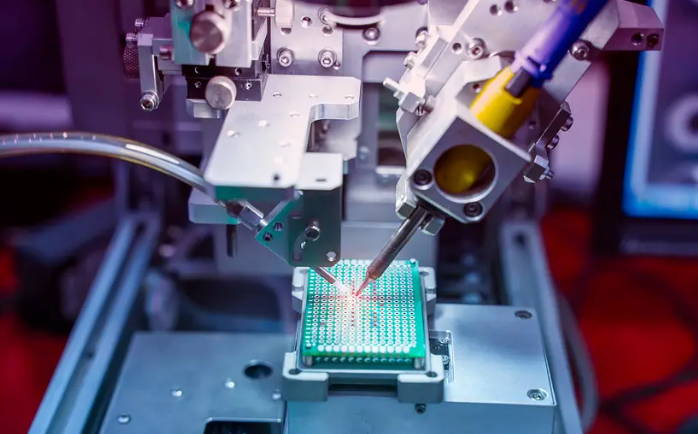
What Quality Checks Are Required for PCB Medical Test in Life-Critical Equipment?
PCB Medical Test protocols for life-critical equipment extend far beyond standard electrical validation to encompass comprehensive safety, reliability, and performance verification under simulated use conditions. These rigorous testing regimens are essential for ensuring that medical PCBs will perform flawlessly throughout their service life, particularly in applications where failure could directly impact patient safety or diagnostic accuracy .
The risk-based approach governing medical PCB testing aligns with international standards including IEC 60601-1 for medical electrical equipment safety and ISO 14971 for application of risk management to medical devices. This methodology requires identifying potential failure modes, assessing their severity and probability, and implementing appropriate verification measures to reduce risks to acceptable levels. For life-critical equipment, this typically involves more extensive testing with stricter acceptance criteria than commercial or even industrial applications .
Essential Medical PCB Testing Protocols
- Electrical Safety Testing: Medical PCBs must undergo rigorous electrical safety validation including dielectric withstand testing (typically 1500V AC for 60 seconds), insulation resistance testing (≥100MΩ at 500V DC), and leakage current measurements (≤100μA for patient-connected parts). These tests verify that the PCB provides adequate isolation between hazardous voltages and accessible parts, preventing electrical shock hazards to patients or operators .
- Biocompatibility Assessment: For PCBs or components that may contact patients either directly or indirectly, biocompatibility testing per ISO 10993 standards is essential. This evaluation determines whether materials release substances that could cause toxic, inflammatory, or allergic reactions when exposed to the body. While the PCB substrate itself may not contact patients, associated connectors, enclosures, or assemblies often require this validation .
- Environmental Stress Testing: Medical PCBs undergo accelerated aging through environmental stress tests including thermal cycling (typically -40°C to +85°C for hundreds of cycles), humidity testing (85°C/85% RH for 168+ hours), and mechanical shock/vibration testing. These conditions validate that the PCB will withstand transportation, storage, and use environments without degradation of performance or reliability .
- Signal Integrity and EMC Validation: For diagnostic equipment particularly, signal integrity testing ensures that low-level physiological signals aren’t corrupted by noise or distortion. Electromagnetic compatibility (EMC) testing verifies that the PCB neither emits excessive electromagnetic interference nor is susceptible to interference from other equipment, both critical considerations in medical environments filled with sensitive electronic devices .
- Sterilization Compatibility: Medical equipment intended for sterile environments or reusable applications must withstand repeated sterilization cycles without degradation. Testing validates PCB survival after exposure to autoclaving, gamma radiation, ethylene oxide, or other sterilization methods appropriate to the intended use environment .
- Long-Term Reliability Demonstration: Life-critical medical equipment often requires demonstrated reliability over extended service periods. Accelerated life testing subjects PCBs to elevated stress conditions (temperature, voltage, operation cycles) to simulate years of service in a compressed timeframe, providing statistical confidence in long-term performance .
- Manufacturing Process Validation: The processes used to manufacture medical PCBs themselves require validation to ensure consistent results. This includes solder process verification, cleanliness testing (ionic contamination levels), and microsection analysis to confirm internal integrity of plated through-holes and multilayer connections .
Table: Medical PCB Testing Requirements by Device Classification
| Test Category | Class A (Non-Critical) | Class B (Therapeutic) | Class C (Life-Support) |
|---|---|---|---|
| Electrical Safety | Basic dielectric withstand | Enhanced isolation testing | Redundant protection systems |
| Environmental Testing | 100 thermal cycles | 200 thermal cycles | 500+ thermal cycles |
| EMC Testing | Basic emissions/susceptibility | Enhanced immunity testing | Military-grade immunity levels |
| Biocompatibility | As required by application | Full ISO 10993 evaluation | Extensive ISO 10993 testing |
| Software Validation | Basic functionality check | Requirements-based testing | Full lifecycle validation |
The comprehensive testing required for medical PCBs in life-critical equipment represents a significant investment in time and resources, but this rigor is essential for ensuring patient safety and device efficacy. By implementing these structured testing protocols throughout the development process—from initial prototype validation through production lot testing—medical device manufacturers can demonstrate compliance with regulatory requirements while delivering the reliability expected in healthcare applications .
How to Select the Right Medical Equipment PCB Supplier to Support Mass Production?
Medical Equipment PCB Supplier selection for mass production requires a systematic evaluation process that balances technical capabilities, quality systems, regulatory compliance, and business factors specific to volume manufacturing. Unlike prototype or low-volume suppliers, production partners must demonstrate scalability, process control, and supply chain management capabilities that ensure consistent quality across thousands or millions of devices while meeting delivery commitments .
The supplier qualification process should begin early in the medical device development cycle, allowing time for thorough evaluation rather than making selection decisions under the pressure of imminent production deadlines. A structured approach involving documented assessments, facility audits, and sample evaluation provides the objective data needed to identify partners capable of supporting your device through its entire product lifecycle .
Key Selection Criteria for Medical PCB Production Partners
- Medical Industry Experience and References: Prioritize suppliers with demonstrated experience producing similar volumes and types of medical PCBs. Request references from comparable medical device companies and follow up to verify performance metrics including on-time delivery, quality levels, and responsiveness to issues. Evidence of successful FDA or other regulatory audits of the supplier’s facility provides additional confidence in their medical market capabilities .
- Certifications and Quality Systems: Verify current certifications including ISO 13485 (medical devices quality management systems) and ISO 9001, with certificates issued by accredited registrars. Review the supplier’s quality manual, process control documentation, and corrective action/preventive action (CAPA) system to ensure alignment with medical device industry standards. For devices requiring biocompatibility, confirm appropriate ISO 10993 certification or testing partnerships .
- Technical Capabilities and Capacity: Assess whether the supplier’s equipment, processes, and technical expertise match your product requirements, including layer count, density, materials, and special technologies like HDI or rigid-flex. Evaluate capacity utilization to ensure they can accommodate your production volumes without compromising quality or delivery lead times. Inquire about equipment maintenance programs and technology roadmaps to ensure future compatibility .
- Supply Chain Management and Material Traceability: Medical device manufacturing requires rigorous material control and full traceability. Evaluate the supplier’s component authentication processes, material certification systems, and lot traceability capabilities. Assess their supply chain resilience for critical components and materials, including alternative sourcing options and inventory management strategies that prevent production interruptions .
- Testing and Validation Capabilities: Volume production requires robust statistical process control rather than piece-part inspection. Review the supplier’s test strategies, including automated optical inspection (AOI), X-ray inspection, flying probe testing, and functional test fixtures. For medical devices, ensure they have experience with the specific testing requirements your product will need for regulatory compliance .
- Cost Structure and Value-Added Services: While unit price is important, consider total cost of ownership including yield rates, payment terms, and additional services like design support, component management, and logistics. Evaluate their value engineering capabilities—the ability to suggest design modifications that reduce cost without compromising quality or performance .
- Communication and Project Management: Assess the supplier’s communication protocols, including escalation procedures, regular performance reviews, and customer notification processes for any process or material changes. Evaluate their project management approach for new product introduction (NPI) and their ability to support design transfers from prototype to production .
Selecting the right medical equipment PCB supplier requires balancing these various factors according to your specific device requirements, risk profile, and business objectives. The most successful partnerships often involve transparent communication, well-defined expectations, and collaborative problem-solving approaches that extend beyond a simple customer-vendor relationship to true partnership in bringing medical innovations to market .
Why Select EBest Circuit (Best Technology) as Your Reliable China Medical Equipment PCB Manufacturer?
EBest Circuit (Best Technology) stands as a premier choice for medical equipment PCB manufacturing by combining international quality standards with cost-effective production capabilities specifically tailored for the healthcare industry. Our commitment to reliability, rapid delivery, and medical-grade quality makes us an ideal partner for device manufacturers seeking to leverage Chinese manufacturing advantages without compromising on safety or performance .
Distinctive Advantages for Medical PCB Manufacturing
- Medical-Grade Manufacturing Facilities: Our manufacturing facilities maintain Class 100,000 cleanroom environments for medical PCB production, with specialized areas for high-reliability applications. We operate under ISO 13485 and ISO 9001 quality management systems with processes specifically validated for medical device manufacturing, ensuring consistent compliance with global regulatory requirements .
- Comprehensive Medical PCB Expertise: With over a decade of specialized experience in medical PCB manufacturing, we have developed deep expertise in healthcare technologies including rigid-flex solutions for portable devices, high-density interconnects for miniaturized implants, and high-frequency boards for imaging equipment. Our engineering team provides valuable design-for-manufacturability feedback specifically tailored to medical standards and requirements .
- Rapid Delivery Capabilities: We have optimized our processes for medical device timelines, offering industry-leading rapid prototyping services with 24-48 hour turnarounds for critical design iterations. Our flexible manufacturing approach accommodates both urgent low-volume production and scalable mass manufacturing, ensuring your medical devices reach clinical evaluation and market deployment without unnecessary delays .
- Stringent Quality Assurance: Beyond standard electrical testing, we implement medical-specific validation including comprehensive materials traceability, biocompatibility verification, and sterilization-compatibility testing. Our reliability protocols simulate years of service through accelerated life testing to ensure stable, long-term performance for life-critical medical equipment. In addition, we support full 3Q qualification reporting—IQ (Installation Qualification) to verify equipment setup and environmental readiness, DQ (Design Qualification) to confirm the PCB design meets functional and regulatory requirements, and PQ (Performance Qualification) to validate consistent production quality under real manufacturing conditions. These combined measures provide medical customers with a verifiable and auditable assurance framework aligned with global healthcare standards.
- Responsive Customer Support: We assign dedicated project managers with medical industry experience to each account, ensuring clear communication and expert guidance throughout the manufacturing process. Our responsive engineering support team is available to address technical questions and implement design changes quickly, minimizing disruptions to your development timeline .
At EBest Circuit (Best Technology), we understand that medical PCBs form the foundation of devices that impact patient outcomes. This understanding drives our commitment to excellence in every aspect of our medical manufacturing services. Pls feel free to contact us at sales@bestpcbs.com to discuss how we can support your specific medical device requirements with reliable, high-quality PCBs delivered on accelerated timelines.

To conclude, Medical Equipment PCB manufacturing represents a specialized segment where quality, reliability, and regulatory compliance directly impact patient care and device efficacy. This comprehensive examination has highlighted the critical considerations from initial design through volume production, emphasizing the importance of selecting manufacturing partners with specific medical industry expertise and proven capabilities.
The journey from concept to mass production involves numerous decision points where medical-specific requirements must take precedence. By understanding these requirements and partnering with manufacturers who specialize in medical PCBs, device companies can accelerate development timelines while ensuring the reliability and safety essential in healthcare applications. EBest Circuit (Best Technology) combines these medical manufacturing capabilities with cost-effective production and rapid delivery options, making us an ideal partner for your medical device PCB requirements. Pls feel free to contact us at sales@bestpcbs.com to discuss how we can support your specific medical device manufacturing needs.