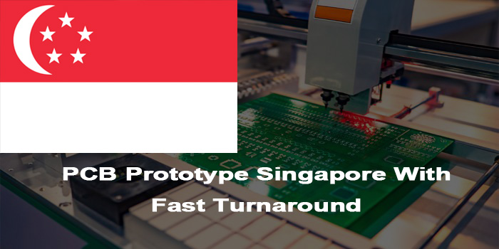
When searching for a PCB fabrication manufacturer, the core challenge lies in balancing quality, lead time, and cost without compromising reliability. EBest is your top choice for a PCB fabrication manufacturer—we combine cutting-edge technology, strict quality control, and flexible customization to meet all your electronic project needs. This guide breaks down critical factors, technical insights, and common pitfalls to help you make an informed decision.
PCB Fabrication Manufacturer
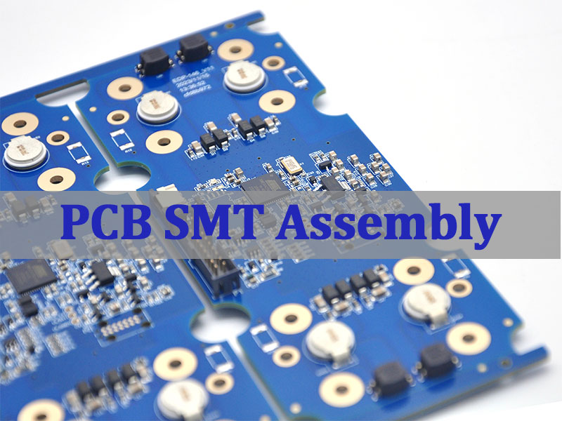
Why Choose EBest as Your PCB Fabrication Manufacturer?
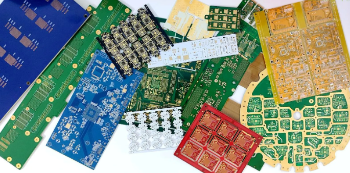
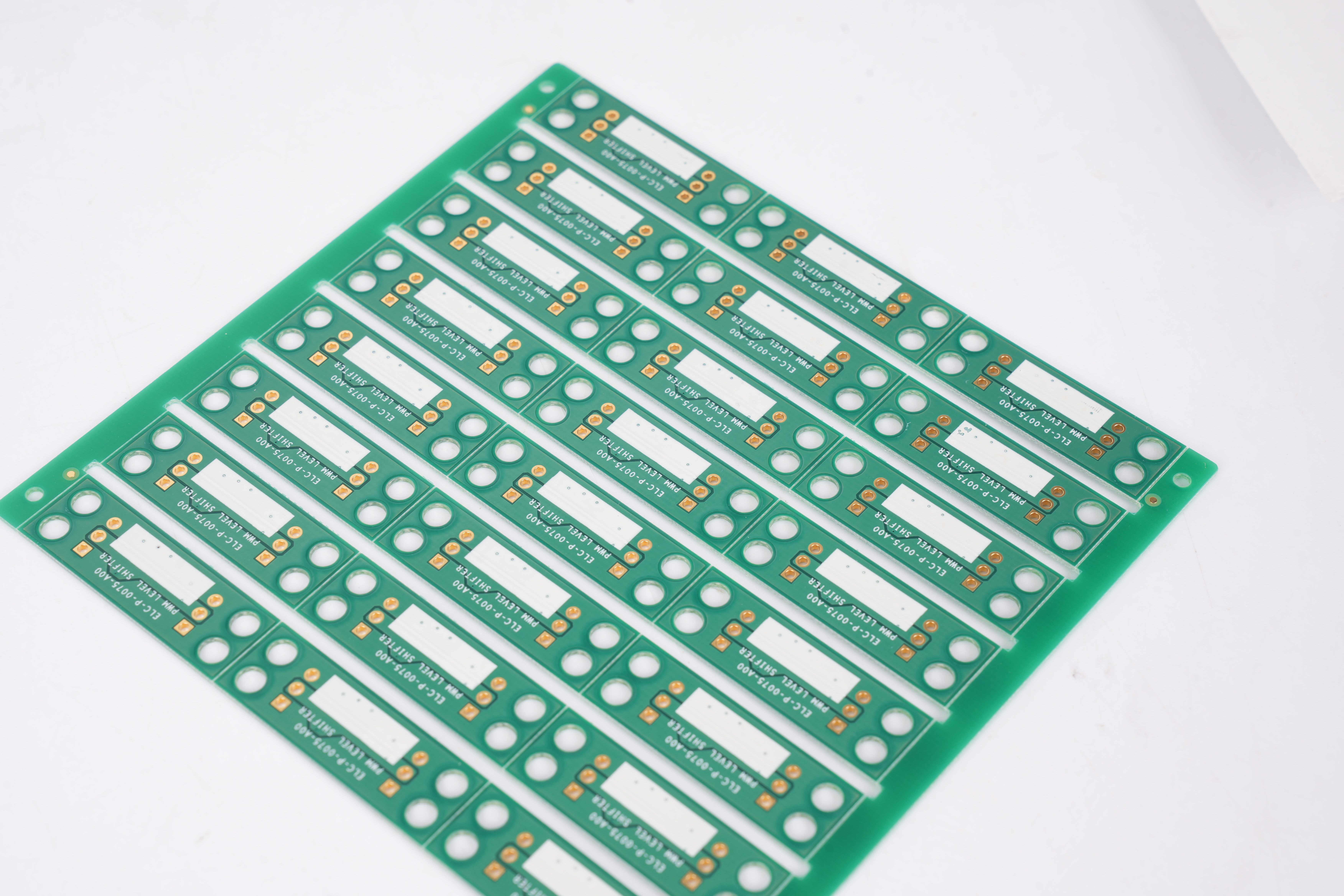
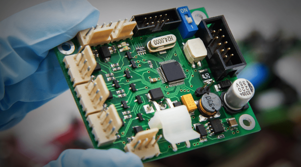
EBest stands out among PCB fabrication manufacturers with three core advantages. First, our technical capabilities cover multilayer boards (up to 32 layers), HDI, high-frequency Rogers boards, and aluminum substrates, supporting custom requirements like impedance control (±5%) and thick copper (3-6OZ). Second, we maintain a 99.8% yield rate through AOI, X-Ray, and VNA testing, complying with IPC Class 2/3 and ISO 9001, UL, RoHS certifications. Third, we offer 24-hour prototyping and 7-10 day batch production, with a 99.9% on-time delivery rate to accelerate your time-to-market.
Why Choose EBest
What Factors Should You Evaluate in a PCB Fabrication Manufacturer?
Technical Capabilities & Equipment
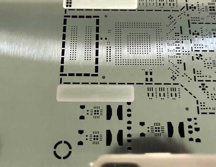
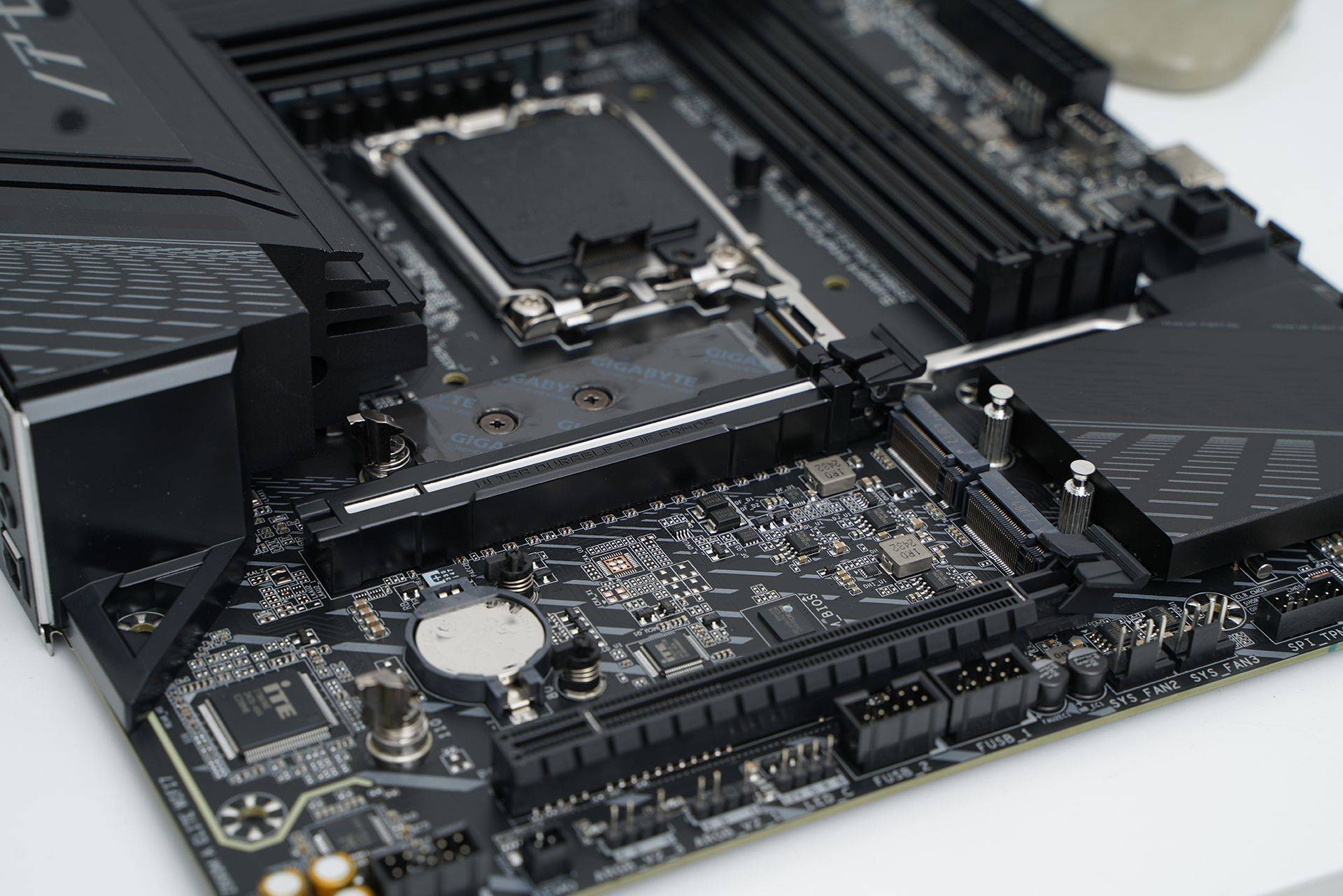
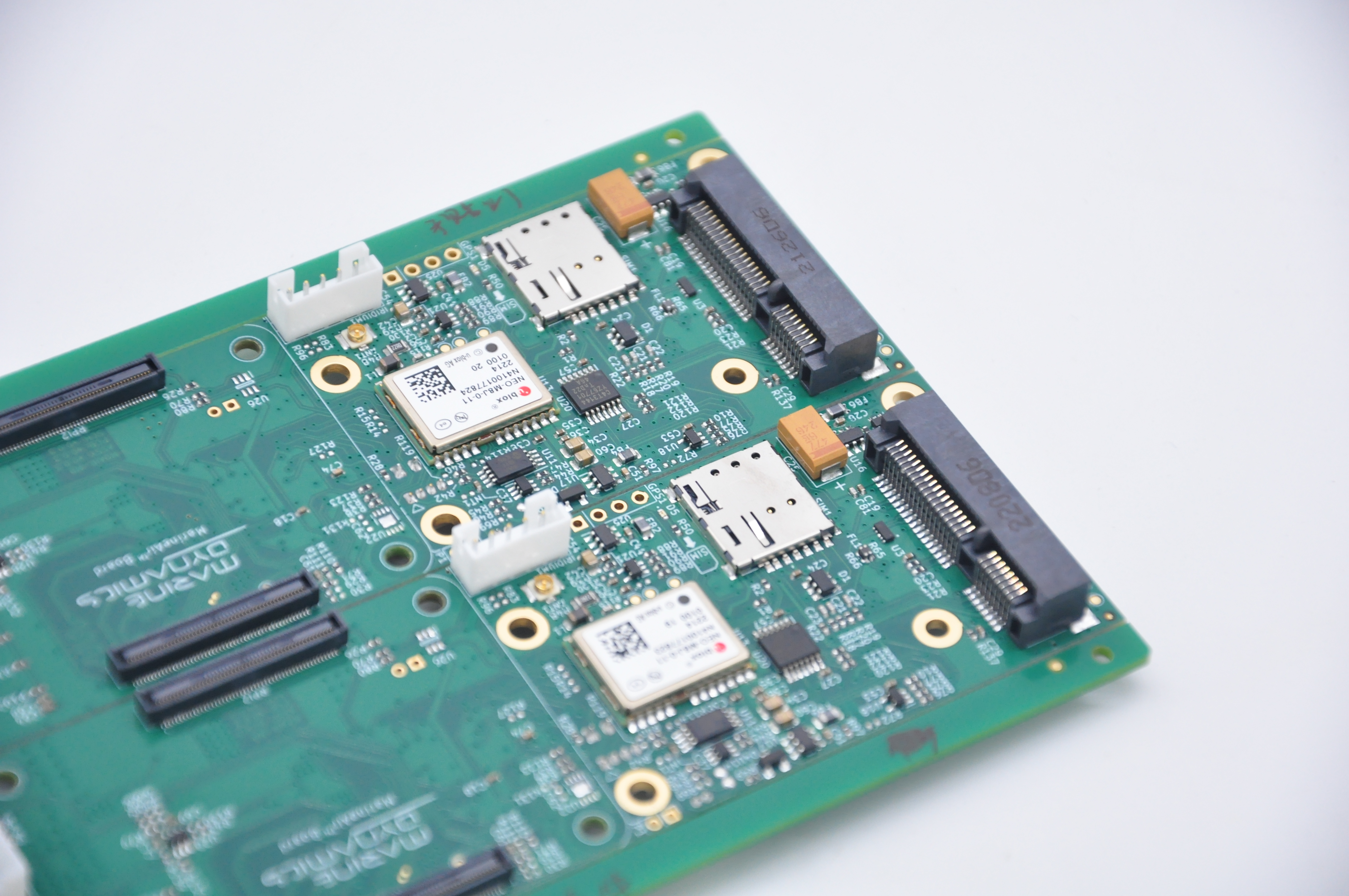
A qualified PCB fabrication manufacturer must have advanced equipment and comprehensive process coverage. Prioritize those with laser drilling machines, automatic plating lines, and plasma desmear equipment to handle complex designs. EBest’s production line supports rigid, flex, and rigid-flex PCBs, with tolerance control as tight as ±0.05mm for drilling precision.
Quality Assurance & Certifications
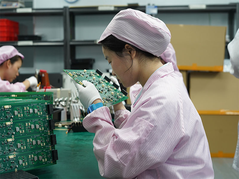
Certifications reflect a manufacturer’s credibility. Essential certifications include ISO 9001 (quality management), IATF 16949 (automotive grade), and UL (safety). EBest conducts 100% AOI inspection for each batch, plus thermal shock and vibration tests to ensure reliability in extreme environments.
Lead Time & Scalability
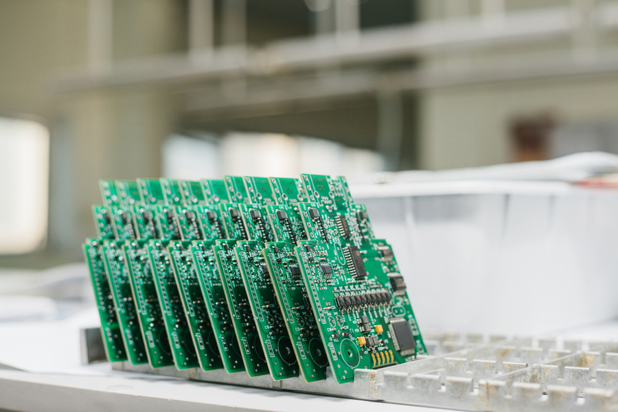
Rapid prototyping and flexible scalability are non-negotiable. EBest delivers prototypes in 24 hours for standard boards and scales from small batches (10pcs) to mass production (1M+ pcs) seamlessly, adapting to your project’s growth.
How to Compare PCB Fabrication Manufacturers Effectively?
Use the following table to compare key metrics of different PCB fabrication manufacturers, avoiding low-cost traps that sacrifice quality.
| Evaluation Metric | EBest Standard | Low-Quality Manufacturer | Industry Average |
|---|---|---|---|
| Yield Rate | ≥99.8% | ≤95% | 97-98% |
| Prototyping Lead Time | 24 Hours | 5-7 Days | 3-4 Days |
| Certifications | ISO 9001, UL, RoHS, IATF 16949 | No Formal Certifications | ISO 9001, RoHS |
| Technical Support | 7×24 Hours, 2-Hour Response | No After-Sales Support | Working Hours Support |
| Material Quality | TG170 FR4, Rogers, High-Quality Copper Foil | Low-Grade Recycled Materials | TG140 FR4 |
What Are the Common PCB Fabrication Defects and Solutions?
Short Circuits (Bridging)
Short circuits are caused by incomplete etching, solder mask offset, or excessive solder. Resolve them by optimizing etching parameters (time/concentration), increasing solder mask bridge width to >0.1mm, and designing stencil openings to reduce solder volume. EBest’s automated etching line ensures uniform copper removal to avoid this issue.
Open Circuits (Breakage)
Open circuits stem from substrate scratches, drilling deviations, or over-etching. Fixes include strengthening material handling, calibrating drilling equipment to ±0.05mm precision, and controlling etching rate. EBest uses laser drilling and real-time process monitoring to minimize such defects.
Board Blistering & Delamination
Blistering results from material moisture absorption, excessive thermal stress, or poor resin curing. Prevent it by storing PCBs in vacuum packaging (≤30% RH), using low-CTE substrates, and limiting lead-free soldering peak temperature to <260℃. EBest pre-bakes all materials before production to remove moisture.
How to Optimize PCB Design for Manufacturability (DFM)?
DFM optimization reduces production defects and costs. As a professional PCB fabrication manufacturer, EBest recommends the following key points:
- Add teardrop transitions to pads to enhance copper foil adhesion and prevent pad lifting.
- Control line width and spacing: minimum 0.1mm for line width, 0.1mm for spacing (IPC Class 2).
- Place ground vias every λ/20 for high-speed signals to reduce EMI interference.
- Provide Gerber files (.gb/.zip) instead of design source files (PADS/Altium) for stable production.
- Mark impedance requirements clearly, and collaborate with the manufacturer to select appropriate materials and stack-ups.
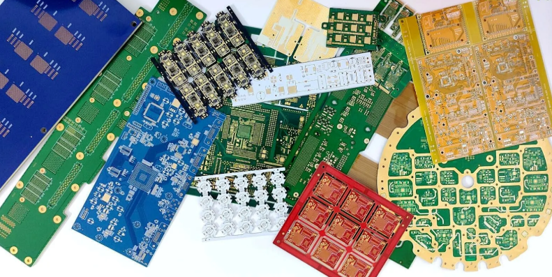
What Is the Cost Structure of PCB Fabrication?
PCB fabrication costs depend on material, layer count, size, quantity, and special processes. The main components include substrate cost (30-40%), copper plating (15-20%), solder mask/surface treatment (10-15%), processing fees (20-25%), and testing fees (5-10%). EBest offers transparent pricing with tiered discounts for large batches, avoiding hidden costs.
Which Surface Treatment Is Best for Your PCB Project?
Surface treatment affects solderability, corrosion resistance, and lifespan. The table below compares common options to help you choose:
| Surface Treatment | Advantages | Disadvantages | Suitable Scenarios |
|---|---|---|---|
| Immersion Gold | Excellent Solderability, Long Shelf Life (12 Months) | Higher Cost | High-End Electronics, Connectors |
| Hot Air Solder Leveling (HASL) | Low Cost, Good Durability | Uneven Surface, Short Shelf Life (3 Months) | Industrial Control, Consumer Electronics |
| Immersion Silver | Smooth Surface, Moderate Cost | Prone to Oxidation | High-Density PCBs, Fast Prototyping |
FAQ About PCB Fabrication Manufacturer
How Long Does PCB Fabrication Take?
Standard prototyping (2-4 layers, 10×10cm) takes 24-48 hours at EBest. Complex boards (HDI, multilayer ≥8 layers) take 3-5 days for prototyping and 7-15 days for mass production. Expedited services are available for urgent projects, with 12-hour turnaround for simple prototypes.
What Certifications Should a Reliable PCB Fabrication Manufacturer Have?
Core certifications include ISO 9001 (quality management), UL (safety compliance), RoHS (environmental protection), and IATF 16949 (automotive grade). For medical electronics, ISO 13485 is required. EBest holds all these certifications to meet global standards.
Can a PCB Fabrication Manufacturer Handle Custom Material Requirements?
Yes. EBest supports custom materials like Rogers (high-frequency), aluminum substrates (heat dissipation), and high-TG FR4 (TG170/TG200) for industrial and automotive applications. Our engineers collaborate with you to select materials matching your project’s performance needs.
How to Verify the Quality of PCB Fabrication?
Verify quality through inspection reports (AOI, X-Ray, impedance test), yield rate data, and reliability test results (thermal shock, vibration). EBest provides a full inspection report for each batch, including IPC-A-600 visual inspection standards compliance.
What File Formats Does a PCB Fabrication Manufacturer Accept?
Most manufacturers accept Gerber files (.gb/.zip) as the standard format. Avoid sending design source files (PADS, Altium) as they may cause compatibility issues. EBest also supports ODB++ files for complex projects and offers DFM checks to optimize file compatibility.
Does EBest Offer One-Stop PCB Fabrication Services?
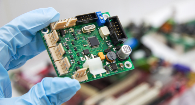
Yes. EBest provides end-to-end services from PCB fabrication to SMT assembly, including component sourcing, soldering, and final testing. This integrated solution reduces lead time and ensures consistency between PCB and assembly quality.
How to Ensure On-Time Delivery from a PCB Fabrication Manufacturer?
Choose a manufacturer with digital production management (ERP/MES systems) for real-time order tracking. EBest uses MES to monitor every production stage, with dedicated project managers updating you on progress. We guarantee a 99.9% on-time delivery rate and provide contingency plans for supply chain disruptions.
Why Is Impedance Control Critical in PCB Fabrication?
Impedance control ensures stable signal transmission in high-speed PCBs (≥1GHz), avoiding signal reflection and distortion. A professional PCB fabrication manufacturer like EBest controls impedance to ±5% precision through material selection, stack-up design, and copper thickness control. This is essential for 5G, AI, and automotive radar applications.
How to Reduce PCB Fabrication Costs Without Sacrificing Quality?
Optimize design to avoid unnecessary complex processes (e.g., blind/buried holes if not required), choose standard materials for non-critical applications, and order in batches to get tiered discounts. EBest’s DFM team provides cost-saving suggestions while maintaining quality, such as optimizing board size to maximize panel utilization.
What After-Sales Support Should a PCB Fabrication Manufacturer Provide?
Reliable after-sales support includes technical consultation, defect analysis, and replacement for qualified quality issues. EBest offers 7×24-hour technical support, 48-hour response to quality complaints, and a one-year warranty for all PCB products. Our engineers help troubleshoot assembly and performance issues to ensure project success.
EBest is a trusted PCB fabrication manufacturer with years of experience serving global clients in automotive, medical, 5G, and industrial sectors. We provide high-quality PCB fabrication services, including prototyping, mass production, and custom solutions. If you need reliable PCB fabrication, place your order with us today via email at sales@bestpcbs.com. Our team will respond within 2 hours to support your project.