If you’ve ever taken a close look at a printed circuit board (PCB), you might have noticed small text, symbols, and lines on the surface. These aren’t just for decoration — they make up the PCB’s silkscreen layer, which plays a key role in making the board readable and easy to assemble. Think of silkscreen as a guiding map that helps technicians identify components and connections quickly. From component labels to polarity indicators, this layer is a simple yet invaluable part of any well-designed PCB. Let’s dive into what silkscreening is, why it’s so useful, and what you need to know about its colors, materials, and application methods.
What is a Silkscreen on a PCB?
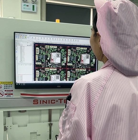
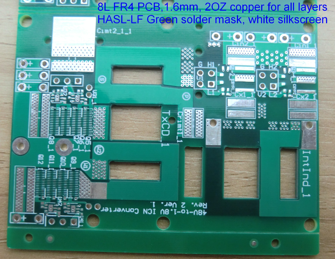
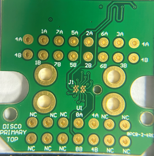
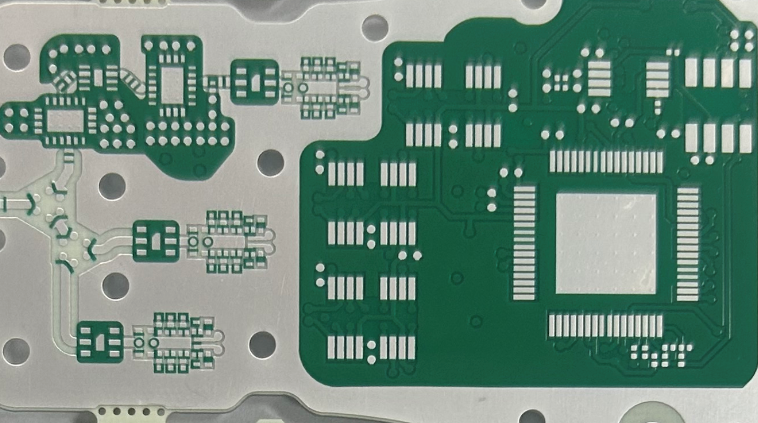
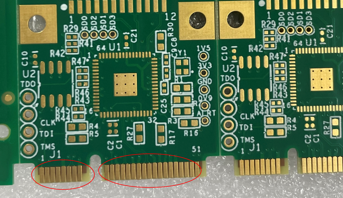
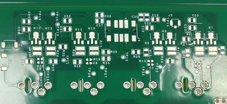
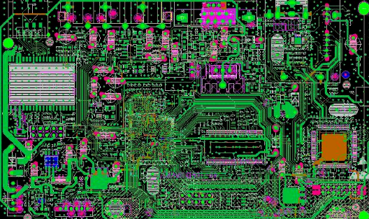
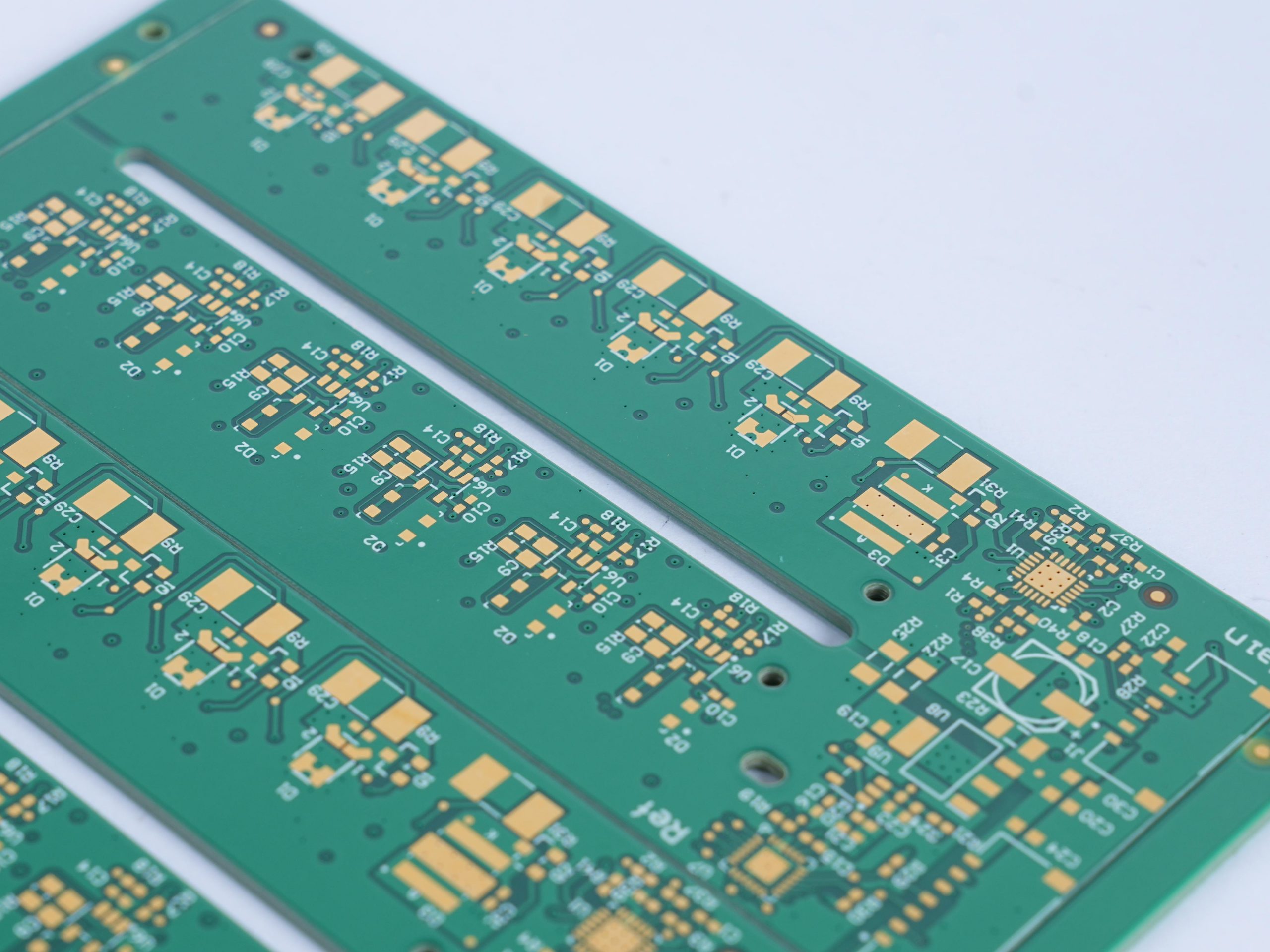
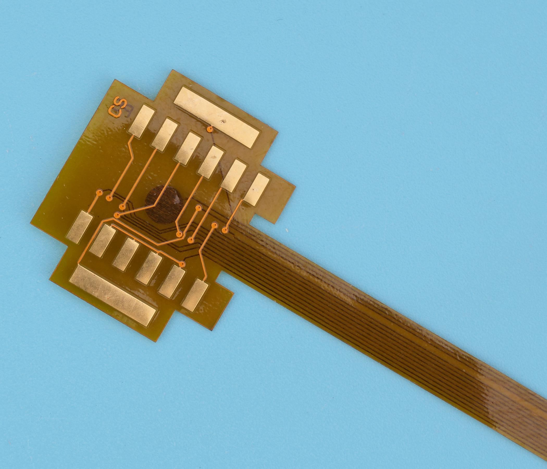
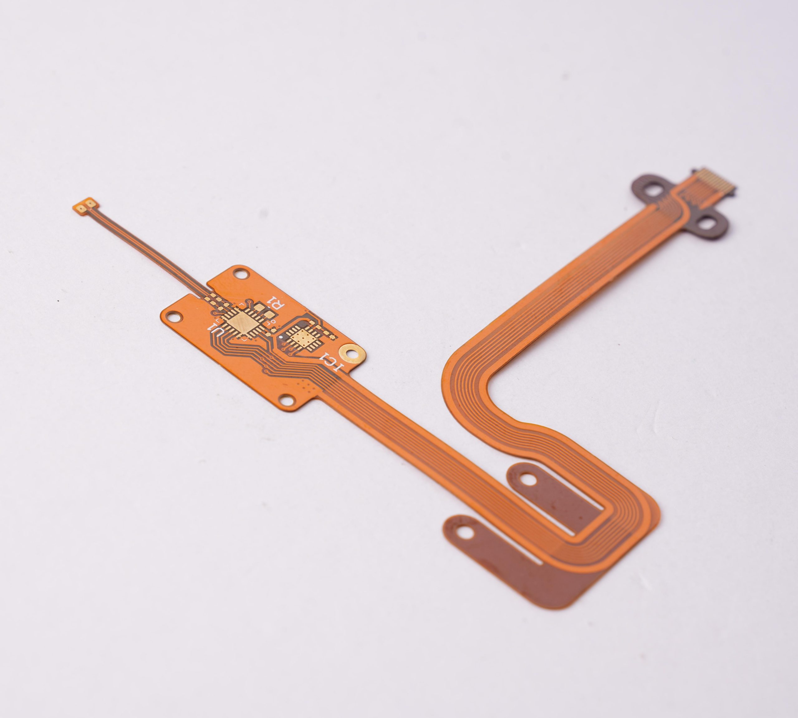
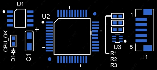
Silkscreen is a layer of ink applied to the PCB’s surface. Typically, you’ll find it on the top side, although it can also be placed on the bottom. Screen silkscreen is usually used to indicate useful information on the PCB board, which can help the user in the assembly process, and is used to mark the component value, part number, polarity and other information, but also contains the version, manufacturer and other information. You’ll often see labels, symbols, and small icons that guide people assembling or repairing the board. In a busy PCB layout, the silkscreen is a roadmap for where everything goes, helping avoid mix-ups and reducing assembly time.
What is the Purpose of Silkscreen?
The silkscreen layer’s primary purpose is to add clarity. By showing clear labels for components, it reduces the chance of error during assembly. When it’s time to troubleshoot, silkscreen also makes life easier by letting technicians locate parts quickly. Silkscreen may include warnings, brand logos, or model names, all helping to make the board more informative. Essentially, it saves time, improves accuracy, and simplifies the process from start to finish.
Silkscreen Information Include on PCB
Silkscreen can be letters, numbers, text. PCB screen printing is done during the PCB manufacturing process, but is used for the PCB assembly process step. Here are some common information that can be silkscreened.
1. Polarity reference sign
2. Determine the test point
3. Component bit number reference mark
4. Component boundary
5, component pin mark
6. Unique identification number for each board
7. Company logo
8. Version number
9. Date code
10, Manufacturer’s logo, serial number, lot number
11. Warning symbols
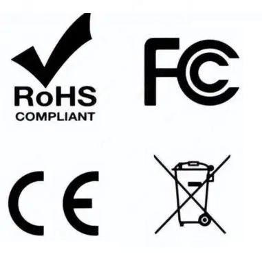
12. Regulatory marks
Regulatory marks are used to indicate that a design has passed inspection or complies with specific regulations. RoHS, FCC, CE and e-waste disposal marks are commonly found on consumer and commercial products that have passed relevant inspections.
If another mark is seen on a design that has been inspected for safety: the UL mark, this mark indicates that the design was manufactured and assembled by a UL-certified manufacturer according to the UL796 and UL94 standards.
What are the Colors of PCB Silkscreen?
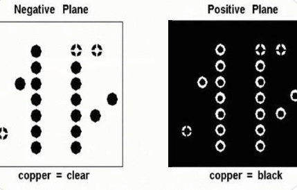
The color of silkscreen is chosen based on readability. White is the most common choice, especially on boards with a green soldermask, because it has a very good readability. And it is a public color and is more friendly to manufacture.
In addition, other colors such as yellow, red, black are also commonly used in the initial stage of PCB board design, pink screen printing is a favorite color of some PCB Layout, but it is usually not recommended to use this color, because it has special characteristics and is not friendly to the manufacturing process.
PCB Silkscreen Symbol
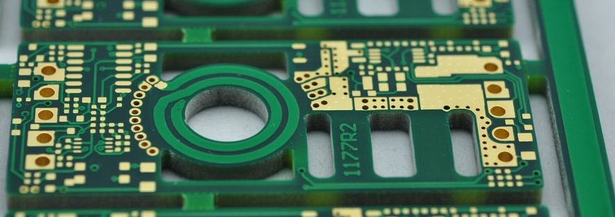
Silkscreen symbols represent various components on the board, making it easier to find specific parts and identify their functions. For instance, “R” stands for resistors, “C” for capacitors, and “U” for integrated circuits. Symbols also show component orientation and polarity, which is crucial for accuracy in assembly. Well-organized symbols on the silkscreen save time and effort, especially during maintenance, as they allow technicians to pinpoint components instantly.
What is the Difference Between Silkscreen and Solder Mask?
Solder mask is a green or other color layer coated on the circuit board, which can play a role in protecting the board. Because there are usually many wires and components on the surface of the circuit board, it is easy to have problems such as short circuit or virtual welding during the welding process, which will lead to damage to the circuit board. Solder resistance layer can effectively avoid the occurrence of this problem. At the same time, the solder resistance layer can also improve the corrosion resistance and mechanical strength of the circuit board.
Solder mask and silkscreen are both coated on the circuit board, but their roles are different. The solder resistance layer is mainly used to protect the circuit board from welding problems, and the screen printing is used to identify the components and related information on the circuit board. In addition, the solder mask is usually green or other bright colors, and the screen printing is usually white or other light colors for easy identification.
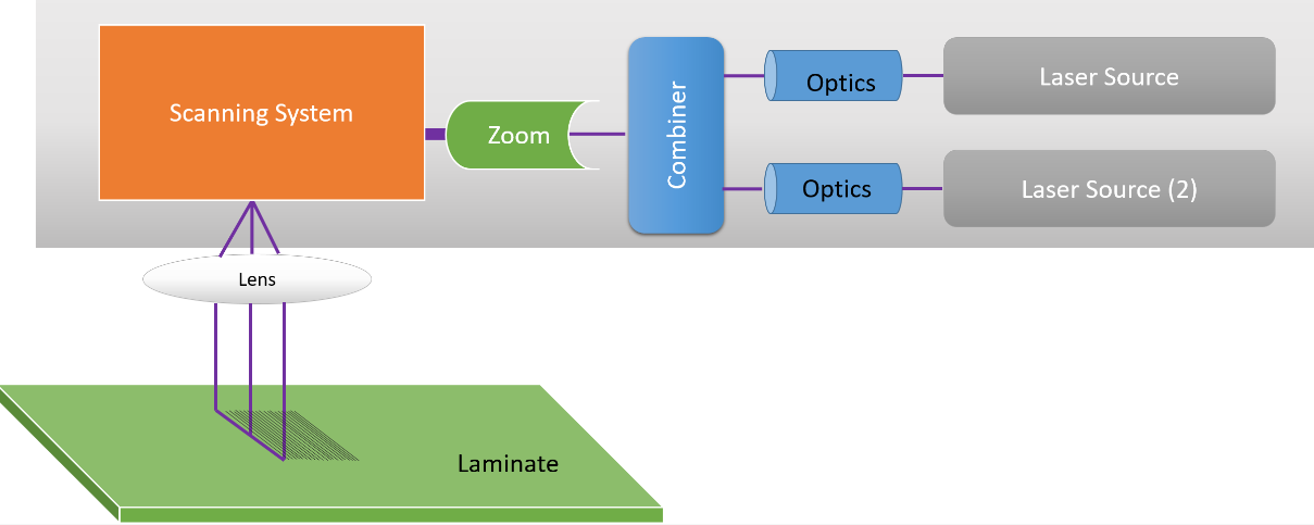
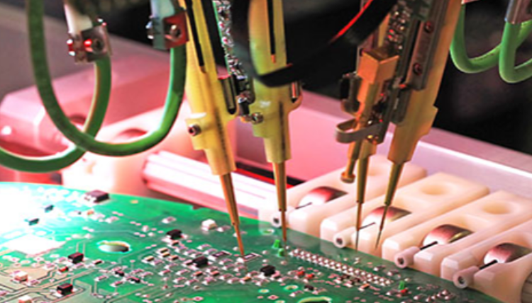
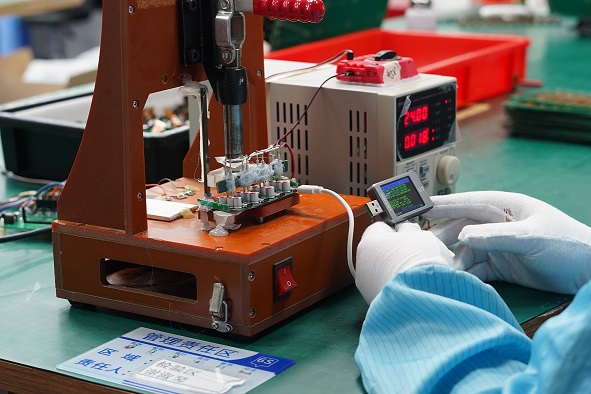
What is the Screen Printing Method of PCB?
There are totally three ways to print silkscreen on a PCB surface, manual screen printing, LPI, and DLP. Let me introduce them for you:
1. Manual screen printing
Do this on the PCB when the registration tolerance is 0.005 inches or the line width is greater than 0.007 inches. Perform manual screen printing using a mold containing text and traces. Traces are made of nylon. The ink is directed to the layer or laminate by stenciling. Next, the ink is cured in a baking oven. This is one of the easy ways to create a silk-screen layer, and it also supports large fonts. Perfecting the art can take years.
2. Liquid Photo Imaging (LPI):
This method is used to screen print threads larger than 4 million. The process of LPI is almost the same as the application of solder mask. In this method, however, the laminate is coated with epoxy resin and then placed under ultraviolet light. The plate is cured and then developed. This method ensures greater accuracy than manual screen printing.
LPI uses white, which requires more ink than the other two types of screen printing. Such prints take a long time to set up.
3. Direct Legend Printing (DLP):
This is one of the other three processes that is expensive. In this process, an inkjet projector and acrylic ink will be used. The ink is applied to the PCB using CAD software. The ink is then exposed to ultraviolet light. Acrylic links are not suitable for PCBS that may have a silver surface.
How Thick is the Silkscreen on a PCB?
Silkscreen thickness is usually about 0.02 mm. This thin layer is enough to make the markings visible without interfering with the board’s layout or operation. The thinness is key because it keeps the board easy to handle without any obstruction or interference, but it’s thick enough that it won’t wear off easily during normal use.
EBest Circuit (Best Technology) highly specialized not only in quick-turn PCB prototype and PCB assembly, but also medium and small volume PCB fabrication. We can provide silkscreen on your PCBs for you with various colors, and we will try our best to meet the demands of silkscreen. If you have any questions, please feel free to contact us, we will be happy to help you.