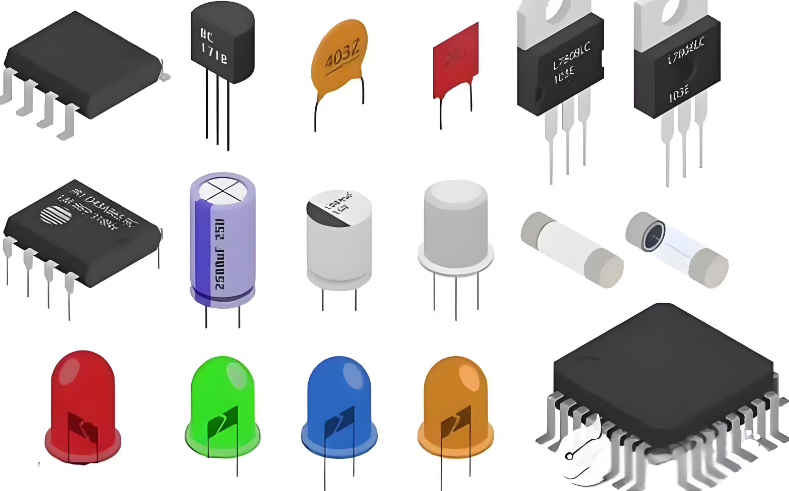
Component sourcing determines whether your PCB project moves forward smoothly or gets delayed by shortages, cost spikes, or quality risks. The right sourcing strategy ensures stable supply, controlled costs, and consistent product performance.
Why Smart Buyers Choose EBest Circuit for Component Sourcing?
Finding components is easy. Securing authentic, cost-effective, and on-time supply is the real challenge. At EBest Circuit, component sourcing is engineered as a controlled system rather than a purchasing task.
What You Get:
Verified supply chain only – no gray market risk
Fast quotation within 24–48 hours
Global sourcing coverage (Digi-Key, Mouser, Arrow, Avnet, etc.)
Free alternative component recommendations
Full traceability down to batch level
Incoming inspection + functional verification
Seamless integration with PCB assembly
Why It Matters:
Reduce procurement uncertainty
Avoid counterfeit components
Stabilize production timelines
Improve product reliability
If your current sourcing process involves chasing suppliers, comparing quotes manually, or dealing with delays, this is where a structured sourcing partner changes everything.
Component Sourcing
What Is Component Sourcing in Modern Electronics Manufacturing?
Component sourcing is no longer a simple purchasing activity. It is a multi-layer decision process involving engineering validation, supplier qualification, lifecycle analysis, and logistics coordination.
In practical terms, it includes:
Identifying exact or equivalent parts
Verifying availability and lifecycle status
Comparing global pricing
Ensuring compliance (RoHS, REACH)
Managing supplier reliability
Coordinating delivery schedules
For complex PCB assemblies, sourcing errors can lead to:
Assembly delays
Yield loss
Redesign costs
Field failures
This is why professional component sourcing directly impacts your product success rate.
Electronic Component Sourcing Services
A robust component sourcing service simplifies complex supply chain operations while improving procurement efficiency. Instead of dealing with multiple vendors, fluctuating prices, and uncertain lead times, manufacturers benefit from a centralized and controlled sourcing system.
This structured approach ensures consistency in quality, cost, and delivery performance across every project stage.
What Factors Influence Component Sourcing?
Effective component sourcing depends on several external and internal variables. Understanding these factors helps reduce risk and maintain stable production.
1. Market Supply and Demand
The semiconductor and passive component markets are highly volatile. Demand surges in sectors like automotive electronics or IoT can quickly lead to shortages, extended lead times, and pricing pressure.
2. Component Lifecycle Management
Every component follows a lifecycle, from introduction to obsolescence. Selecting parts close to EOL (End-of-Life) increases long-term risk and may force costly redesigns.
3. Supplier Credibility
Supplier selection directly affects product quality. Unverified vendors can introduce counterfeit or substandard parts. Working with ISO-certified and authorized distributors significantly reduces these risks.
4. Logistics and Lead Time Stability
Global transportation, customs clearance, and geopolitical changes can all impact delivery timelines. Strategic planning and buffer strategies are essential to maintain continuity.
5. Pricing Fluctuation
Component pricing can shift rapidly due to wafer supply constraints or raw material costs. Strategic sourcing agreements help stabilize procurement budgets.
6. Quality Assurance Systems
Even a minor component defect can lead to system failure. Reliable component sourcing includes incoming inspection, functional verification, and traceability control.
At EBest Circuit, these factors are integrated into a data-driven sourcing model, ensuring an optimal balance between cost, quality, and lead time.
How to Handle Component Shortages Effectively?
Component shortages remain one of the most critical challenges in electronics manufacturing. A proactive sourcing strategy can significantly reduce their impact.
1. Alternative Component Strategy
When original parts are unavailable, engineers evaluate compatible substitutes based on electrical, thermal, and mechanical parameters. This ensures functional consistency without redesign risks.
2. Demand Forecasting and Early Procurement
Sharing forecasts with suppliers allows capacity reservation in advance. This reduces exposure to sudden shortages.
3. Authorized Procurement Channels
Sourcing through authorized distributors ensures authenticity and traceability. This is especially critical in regulated industries such as medical and automotive electronics.
4. Global Supplier Network
Diversifying sourcing across regions reduces dependency on a single market. EBest Circuit works with leading distributors such as Digi-Key, Mouser, Arrow, and Avnet to ensure stable supply coverage.
5. Strategic Inventory Management
Maintaining buffer stock for long-lead or high-risk components improves flexibility and prevents production delays.
Our sourcing team continuously monitors global supply conditions and updates internal databases, enabling faster response and reduced downtime.
How to Get a Component Sourcing Quotation?
A clear and structured process ensures fast and accurate quotations for component sourcing.
Step 1: Prepare a Complete BOM
A well-defined BOM (Bill of Materials) should include:
Manufacturer Part Number (MPN)
Component type and description
Quantity per unit
Package type and specifications
Approved manufacturers or alternatives
Step 2: Submit Your BOM
Send your BOM via email or through our quotation system. Detailed information allows faster and more precise evaluation.
Step 3: Sourcing Evaluation and Quotation
Our team will:
Verify availability and lifecycle status
Compare pricing across authorized distributors
Recommend alternatives if necessary
You will receive a detailed quotation including pricing, lead time, and sourcing channels.
Step 4: Order Confirmation and Procurement
Once approved, orders are placed immediately to secure supply and pricing.
Step 5: Incoming Quality Inspection
All components undergo strict inspection, including:
Visual inspection
Functional testing
Authenticity verification
This ensures full compliance with design and performance requirements before production.
Why Choose EBest Circuit for Component Sourcing?
Component sourcing requires precision, experience, and a reliable network. At EBest Circuit, the focus is not only on procurement but on delivering certainty and consistency.
Strategic Location Advantage: Based in Shenzhen, close to Huaqiangbei, the largest electronic components market in China
Verified Supply Chain: Only authorized and certified suppliers are used
Strict Quality Control: Visual, functional, and X-ray inspections applied to all components
Global Procurement Network: Strong partnerships with leading distributors
Transparent Process: Full visibility of sourcing channels and delivery timelines
Our component sourcing service reduces procurement complexity, shortens lead time, and improves overall project efficiency.
FAQs About Component Sourcing
1. What is required for a component sourcing quotation?
A detailed BOM with MPNs, quantities, and specifications is sufficient. Our team handles the rest of the sourcing process.
2. Can you source obsolete or hard-to-find components?
Yes. We specialize in sourcing EOL and hard-to-find components through a global supplier network.
3. How fast can I receive a quotation?
Typically within 24–48 hours after BOM submission.
4. Are all components tested before use?
Yes. All sourced components undergo inspection and verification before entering production.
5. Do you provide turnkey services including component sourcing?
Yes. We offer full turnkey solutions including PCB fabrication, component sourcing, assembly, testing, and final delivery.
Ready to Simplify Your Component Sourcing?
If you are dealing with unstable supply, long lead times, or inconsistent quality, it is time to upgrade your sourcing strategy.
Best Technology provides reliable component sourcing with full traceability, fast quotation, and global supply support, ensuring your PCB projects move forward without delays.
Send your BOM today and get a fast, accurate quotation: 📧 sales@bestpcbs.com
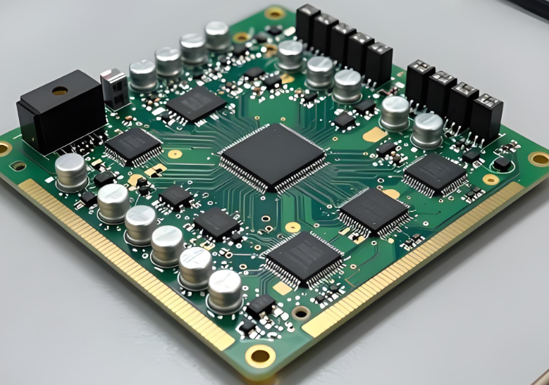
Why EBest Should Be Your Best Box Build Assembly Manufacturers?
Choosing the right partner for box build assembly is not just about cost. It directly affects product reliability, delivery speed, and your brand reputation. Many suppliers can assemble a PCB, but far fewer can deliver a complete, ready-to-use system.
EBest Circuit (Best Technology) focuses on full-process integration. From PCB fabrication to final enclosure assembly, every step is controlled under one system. This reduces communication gaps and prevents costly delays.
What makes EBest stand out is the depth of engineering support and execution consistency. Instead of simply following files, the team actively reviews design, structure, and manufacturability before production starts.
Key strengths include:
20+ years of PCB and PCBA experience
Full turnkey box build assembly services
Free DFM and BOM optimization support
Strong supply chain with global sourcing capability
Fast turnaround with stable quality control
Complete traceability through MES system
All-in-One Turnkey Box Build Assembly
What Is Box Build Assembly?
Box build assembly refers to the complete assembly of an electronic product into its final enclosure. It goes beyond PCB assembly and includes mechanical, electrical, and system-level integration.
So, what does “Box Built” mean? In simple terms, a “box built” product is ready to use right out of the factory.
This typically includes:
PCB assembly (SMT + through-hole)
Cable and wire harness installation
Enclosure or housing assembly
Power supply integration
Display or interface installation
Final system testing
Unlike standalone PCBA, box build assembly delivers a finished product. It is often used in industries where plug-and-play functionality is required.
Box Build Printed Circuit Board Assembly Services
Box build printed circuit board assembly services combine PCB manufacturing, component sourcing, assembly, and system integration into one seamless workflow. At EBest, this service is structured to minimize risk and maximize efficiency. Each stage is tightly connected, which helps avoid mismatches between design and production.
Core service scope includes:
PCB fabrication (FR4, aluminum, ceramic, HDI)
SMT and through-hole assembly
Component sourcing and verification
Cable assembly and harness integration
Mechanical assembly and enclosure fitting
Firmware loading and configuration
Functional testing and system validation
Packaging and logistics
This turnkey model is especially useful for companies that want to avoid managing multiple vendors. Instead of coordinating separate PCB, assembly, and enclosure suppliers, everything is handled in one place.
EBest Circuit’s Box Build Capabilities
EBest offers a comprehensive capability set designed for both low-volume prototypes and mass production.
Manufacturing Capabilities
High-mix, low-volume and medium-volume production
Complex multi-board system integration
Precision mechanical assembly
Cable routing and harness design support
Custom enclosure integration
Technical Capabilities
AOI, X-ray, SPI inspection systems
Functional test development
Burn-in testing for reliability
Firmware programming and configuration
ESD-safe production environment
Supply Chain Capabilities
Global component sourcing
Alternative component recommendations
Cost optimization strategies
Long-term supply planning
Quality and Compliance
ISO9001, ISO13485, IATF16949, AS9100D
Full traceability system
Strict incoming and outgoing inspection
Process control at each production stage
What Is the Box Build Assembly Process?
The box build assembly process is a structured, multi-stage workflow. It integrates electronics, mechanics, and system-level validation. Each step directly impacts product reliability, cost, and delivery speed. A well-controlled process avoids rework and ensures consistency.
Below is a detailed box building assembly process in EBest Circuit:
1. Engineering Review & DFM Optimization
This is the most critical stage. Many downstream issues originate here.
Review Gerber, BOM, and mechanical drawings
Check component availability and lifecycle status
Validate enclosure fit, connector alignment, and tolerances
Perform DFM (Design for Manufacturability) and DFA (Design for Assembly)
Key engineering checks include:
Clearance between PCB and enclosure (typically ≥0.5 mm)
Connector positioning tolerance (±0.1 mm typical)
Thermal path validation for high-power components
At EBest, this stage often includes BOM optimization to reduce cost and avoid supply risks.
2. Supply Chain Preparation
Material readiness determines whether production runs smoothly.
Source components from verified suppliers
Identify alternates for long lead-time parts
Prepare mechanical parts (metal, plastic, die-cast housings)
Verify cable assemblies and connectors
A strong supply chain reduces delays and ensures stable production.
3. PCB Fabrication
The PCB is manufactured based on design requirements.
Layer stack-up construction
Copper thickness control (e.g., 1 oz / 2 oz / heavy copper)
Surface finish (ENIG, HASL, ENEPIG, etc.)
Impedance control for high-speed designs
This stage defines electrical performance and long-term reliability.
4. PCB Assembly (PCBA)
This is the core electronic assembly stage.
Solder paste printing (SPI inspection)
SMT placement using high-speed machines
Reflow soldering with thermal profile control
Through-hole insertion (manual or wave soldering)
Inspection methods:
AOI (Automated Optical Inspection)
X-ray for BGA/QFN components
ICT (In-Circuit Test) if required
Defect control here directly affects final yield.
5. Cable & Harness Assembly
Wiring is often underestimated but critical in box build.
Crimping and soldering of connectors
Cable routing design to avoid EMI and interference
Labeling and identification for traceability
Key engineering concern:
Signal cables should be separated from power cables
Bend radius must meet cable specifications
6. Mechanical Assembly (Box Integration)
This step transforms PCBA into a physical product.
Mount PCB into enclosure using screws or standoffs
Install connectors, switches, displays, and panels
Testing ensures early failure detection and improves field reliability.
9. Final Assembly & Quality Inspection
Before shipment, every unit is verified.
Visual inspection of enclosure and labeling
Torque verification for screws
Final electrical safety check
10. Packaging & Logistics
The final step protects the product and prepares delivery.
Anti-static packaging (ESD protection)
Custom packaging for fragile assemblies
Labeling, barcoding, and traceability records
What Is the Difference Between Box Build and PCBA?
Although closely related, PCBA and box build assembly serve different roles in the manufacturing chain. Understanding the difference helps you choose the right service model.
Below is a more detailed comparison:
Category
PCBA (Printed Circuit Board Assembly)
Box Build Assembly
Definition
Assembly of electronic components onto a PCB
Full product assembly including PCB, enclosure, and wiring
Scope
Electronics only
Electronics + mechanical + system integration
Output
Functional circuit board
Finished, ready-to-use product
Complexity
Moderate
High
Assembly Content
SMT, THT components
PCBA + cables + housing + modules
Mechanical Involvement
None
Extensive (enclosures, brackets, panels)
Wiring
Not included
Includes cable harness and routing
Firmware
Usually not included
Included (programming and configuration)
Testing Level
Board-level testing (AOI, ICT)
Full system testing and validation
Thermal Design
Limited to PCB
Full system thermal management
Supply Chain
Focused on electronic parts
Covers electronics + mechanical + cables
Customization
Limited
High (custom enclosures, system design)
Delivery Form
Semi-finished product
End product ready for use
Typical Use
Intermediate manufacturing stage
Final product delivery
Practical Insight
If you only need a circuit board → choose PCBA
If you need a complete device → choose box build assembly
In many projects, PCBA is just one step within the box build workflow.
Box Build Assembly Applications
Box build assembly services are widely used across industries that require integrated electronic systems. Common applications include:
Industrial Equipment
Control panels
Automation systems
Power distribution units
Medical Devices
Diagnostic equipment
Monitoring systems
Portable medical units
Telecommunications
Network devices
Signal processing units
Communication modules
Automotive Electronics
Control modules
Battery management systems
In-vehicle electronics
Consumer Electronics
Smart home devices
IoT products
Embedded systems
FAQs about Box Build Assembly
1. What exactly is included in a box build assembly service?
Box build assembly, also known as systems integration, covers everything beyond the bare printed circuit board. It typically includes:
Installing the PCBA into a metal or plastic enclosure.
Connecting complex cabling or wire harnesses.
Installing sub-assemblies (like sensors or power supplies) and biological/mechanical components.
Final configuration: Loading software and performing functional testing.
2. What is the difference between PCB assembly and box build assembly?
While PCB assembly (PCBA) focuses strictly on soldering components onto a board, box build is the “complete” process. Think of the PCBA as the “brain” and the box build as the “entire body.” A box build provider manages the mechanical housing and the relationship between the board and its external environment.
3. What information does a manufacturer need for a box build quote?
To provide an accurate quote, a manufacturer generally requires:
Bill of Materials (BOM): Including the enclosure, cables, and even small hardware like screws.
3D CAD Models: To understand the spatial layout.
Assembly Instructions: Detailed steps or “golden unit” photos.
Test Specifications: Clear parameters for what constitutes a “pass” during final functional testing.
4. How does box build assembly impact the total cost of production?
While the unit price is higher than a bare PCBA, a box build often reduces total cost by:
Consolidating shipping (you receive a finished product, not parts).
Reducing your internal labor and overhead for final assembly.
Simplifying the supply chain by having one partner manage multiple vendors for plastics, metals, and electronics.
5. What are the most common challenges in box build projects?
The primary challenges involve tolerances and fit. If the enclosure (often sourced from a different vendor) and the PCBA do not align perfectly due to design variations, the final assembly can fail. Effective providers use Design for Manufacturing (DFM) reviews early on to ensure that cables aren’t pinched and connectors align with the housing cutouts.
6. Is box build assembly suitable for small-batch production?
Yes. Many “High-Mix, Low-Volume” (HMLV) manufacturers specialize in small batches. This is common in the medical and industrial sectors, where precision and traceability (like ISO 13485 standards) are more critical than mass-market speed. Outsourcing small batches allows companies to scale without investing in their own assembly lines.
EBest Circuit (Best Technology) provides a full turnkey solution. From PCB fabrication to final assembly, every step is handled with precision and care.
If you are planning your next project and need a reliable partner for box build assembly, the team is ready to support you.
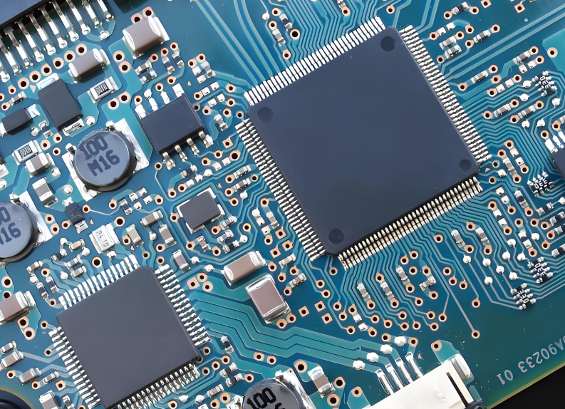
BGA Assembly (Ball Grid Array Assembly) is a PCB assembly process where components are mounted using an array of solder balls underneath the package instead of leads. It provides higher connection density, better thermal performance, and improved electrical reliability, making it ideal for high-speed and high-performance electronics such as CPUs, GPUs, and communication devices.
BGA Assembly is a critical process in modern electronics, enabling high-density, high-speed, and high-reliability PCB designs. In this guide, you will understand BGA PCB assembly from process control to supplier selection, helping you reduce defects and improve production stability.
BGA Assembly
Looking for Reliable BGA Assembly? Why Right Partner Is Important?
Many projects encounter hidden failures during BGA assembly, especially when scaling from prototype to mass production. Since solder joints are located beneath the package, defects cannot be seen directly and often appear only after testing or field use.
Typical challenges include:
Hidden defects such as voids and head-in-pillow
Warpage during reflow causing open joints
Inconsistent yield across production batches
Difficult inspection and rework
Reliability risks under thermal cycling
Because of these risks, selecting the right bga pcb assembly manufacturer becomes a key factor in product success rather than a simple sourcing decision.
EBest Circuit – How We Serve You?
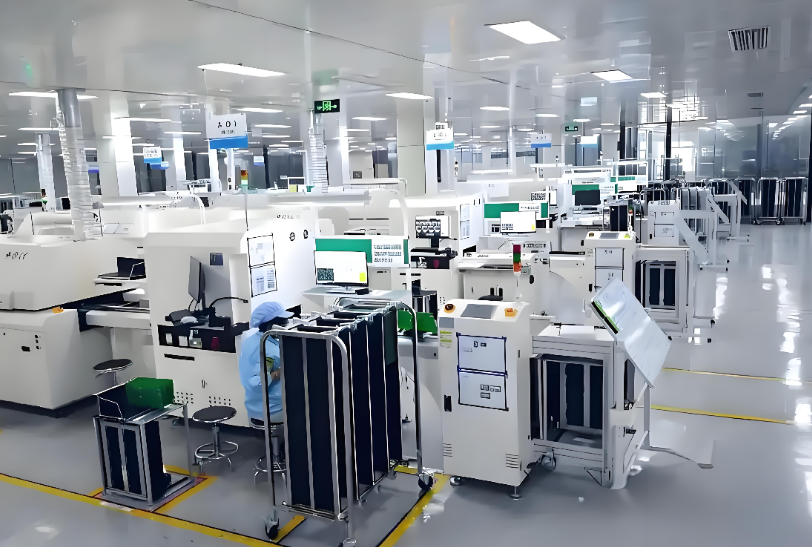
EBest Circuit (Best Technology) provides one-stop bga assembly services, including PCB fabrication, component sourcing, SMT assembly, inspection, and final delivery. With over 20 years of experience, we focus on both engineering support and stable production.
What we provide:
Turnkey BGA PCB assembly service
DFM & DFA support before production
Quick turn prototyping and mass production
Advanced inspection (SPI + X-ray + AOI)
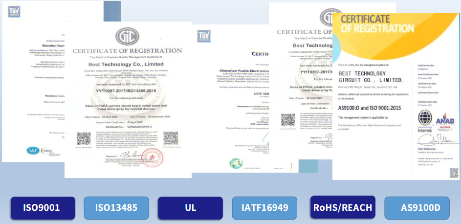
Certified system (ISO9001, ISO13485, IATF16949, AS9100D)
Our goal is not only to assemble boards, but to reduce risk and improve yield from the beginning.
Our BGA Assembly Capabilities
BGA assembly requires precision, process stability, and advanced inspection. Our capability is built around real production control and engineering support.
Technical Capabilities
Minimum BGA pitch down to 0.3 mm
Placement accuracy up to ±25 µm
Support for uBGA, CSP, LGA, PoP, fine-pitch BGA
Double-sided SMT and mixed assembly (SMT + THT + BGA)
HDI, multilayer, and high-speed PCB support
Lead-free and RoHS-compliant processes
Full support from prototype to mass production
100% X-ray inspection available for BGA joints
SPI inspection for solder paste volume control
Multi-zone reflow profiling for thermal consistency
BGA rework capability with dedicated stations
Void rate control typically <10%
Support for tight-pitch, high-density PCB layouts
MSL-controlled component handling
ESD-controlled production environment
Functional testing and validation support
Quick turn service for urgent projects
What Is BGA Assembly and Why Is It Critical in Modern PCB Design?
BGA assembly is a process where components with solder balls are mounted onto PCB pads and soldered during reflow. Compared with traditional packages, BGA provides higher pin density and shorter signal paths.
This makes it essential for:
High-speed signal transmission
Compact electronic devices
Better thermal dissipation
High-performance computing and communication systems
As product complexity increases, BGA PCB assembly becomes a standard requirement rather than an option.
What Makes BGA PCB Assembly So Challenging?
BGA assembly introduces several technical challenges due to its structure and process sensitivity. Even small deviations can lead to hidden defects.
Key challenges include:
Invisible solder joints under the package
Thermal warpage during reflow
Head-in-pillow defects
Solder voids affecting reliability
Complex and costly rework process
Because of these factors, advanced process control and inspection are required.
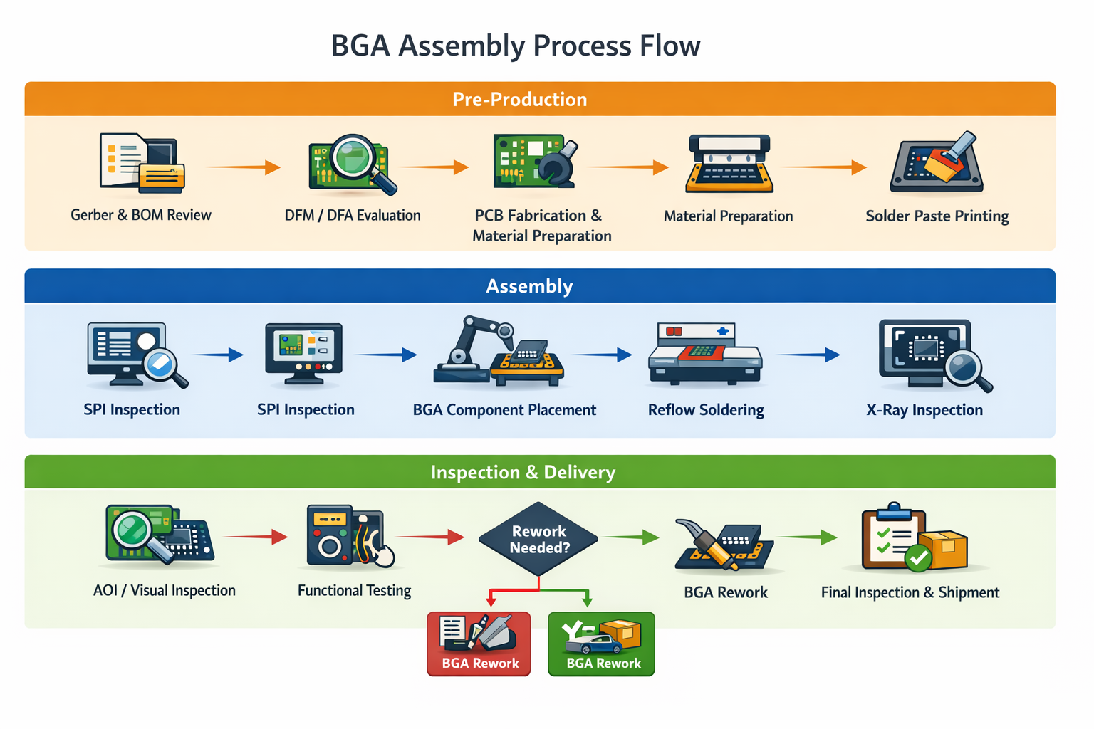
How Does the BGA Assembly Process Work Step by Step?
BGA assembly follows a tightly controlled workflow, because each stage directly affects solder joint reliability and final product performance. A typical BGA PCB assembly process can be summarized as follows:
To make the process easier to understand, each step serves a specific purpose in controlling quality and reducing hidden BGA defects:
1. Gerber & BOM Review First, the engineering team reviews the design files and bill of materials to confirm manufacturability and component availability.
2. DFM / DFA Evaluation Next, design for manufacturability and design for assembly checks are performed, helping identify risks such as pad mismatch, spacing issues, or thermal concerns before production starts.
3. PCB Fabrication & Material Preparation After that, the PCB and components are prepared, while moisture-sensitive devices are handled according to proper storage and baking requirements.
4. Solder Paste Printing Then, solder paste is printed onto the PCB pads with carefully controlled volume, because excessive or insufficient paste can directly affect BGA joint quality.
5. SPI Inspection Before placement, solder paste inspection verifies paste height, area, and consistency, which helps reduce process variation early.
6. BGA Component Placement The BGA device is then placed using high-precision pick-and-place equipment, ensuring accurate alignment between the solder balls and PCB pads.
7. Reflow Soldering Next, the board passes through the reflow oven, where the solder balls melt and form electrical and mechanical connections under a controlled temperature profile.
8. X-ray Inspection Since BGA joints are hidden beneath the package, X-ray inspection is used to check for voids, bridging, opens, and insufficient solder wetting.
9. AOI / Visual Inspection In addition, visible components and surrounding areas are inspected to confirm overall assembly quality.
10. Functional Testing Once inspection is complete, electrical and functional tests are performed to verify that the assembled board works as intended.
11. Rework if Needed If defects are detected, qualified technicians use dedicated BGA rework equipment to remove and replace the component under controlled conditions.
12. Final Inspection & Shipment Finally, the board goes through final quality verification before packaging and shipment.
Each parameter must be tightly controlled to ensure stable solder joints and minimize defects.
What Equipment Is Required for High-Quality BGA Assembly?
Among these, X-ray inspection is essential because it allows detection of hidden solder defects.
China BGA PCB Assembly vs Your Local Manufacturing
Choosing between China BGA PCB assembly and local manufacturing depends on project priorities.
Factor
China
Local
Cost
20–40% lower
Higher
Capability
Advanced
Varies
Lead time
Competitive
Faster locally
Scalability
High
Medium
For many companies, China offers a strong balance between cost and capability.
Which Industries Require Advanced BGA Assembly Services?
BGA assembly is widely used in:
Consumer electronics
Automotive systems
Industrial control
Medical devices
Aerospace
These industries require both performance and reliability.
How to Choose the Right BGA PCB Assembly Manufacturer?
When selecting a partner, focus on both technical capability and process control.
Key factors include:
Proven BGA assembly experience
X-ray and inspection capability
Process control and thermal profiling
Quality certifications
Engineering support
A reliable partner helps reduce defects and improve production consistency.
FAQs about BGA Assembly Services
1. What are the main advantages of BGA over QFP?
The primary advantage of Ball Grid Array (BGA) over Quad Flat Package (QFP) is its higher connection density. Since BGAs use the entire bottom surface for interconnects rather than just the perimeter, they allow for hundreds of pins in a smaller footprint. Additionally, BGAs offer better thermal dissipation and lower parasitic inductance, which improves high-speed signal integrity.
2. Can BGA components be inspected visually?
No, BGA solder joints cannot be inspected with the naked eye or standard optical equipment because they are hidden beneath the component body. To ensure joint integrity, manufacturers use Automated X-Ray Inspection (AXI) to look through the package and detect defects like solder voids, bridging, or insufficient wetting.
3. What is the most common cause of BGA assembly failure?
The most common cause of BGA failure is an incorrect reflow temperature profile. If the temperature rises too quickly or unevenly, it can lead to “popcorning” (internal package cracking due to moisture), solder ball bridging (shorts), or “head-in-pillow” defects where the solder ball and paste fail to merge.
4. Can you hand-solder a BGA package?
While technically possible for advanced hobbyists with a hot air station, hand-soldering BGAs is not practical or recommended for production. BGAs require precise alignment and a specific thermal profile that can only be consistently achieved using automated pick-and-place machines and multi-zone reflow ovens.
5. Why is “underfill” used in BGA assembly?
Underfill is a specialized epoxy resin injected under the BGA package after soldering. It is used to improve the mechanical reliability of the device by spreading the stress of thermal expansion and physical shock (like dropping a phone) across the entire component rather than just the individual solder balls.
6. What is a “Fine-Pitch” BGA?
A Fine-Pitch BGA (FPBGA), sometimes called a MicroBGA, refers to components where the distance between the centers of the solder balls (the “pitch”) is 0.8mm or less. As the pitch decreases to 0.5mm or 0.4mm, the assembly process becomes significantly more challenging, often requiring advanced PCB technologies like “via-in-pad” to route signals.
Ready for Fast and Reliable BGA Assembly? Get a Quote Today
If you are looking for a reliable bga pcb assembly manufacturer, EBest Circuit is ready to support your project.
Through-hole assembly (also known as Thru-Hole Technology or THT) is a printed circuit board (PCB) mounting process where electronic component leads are inserted into pre-drilled holes in the board and soldered to pads on the opposite side. While newer Surface Mount Technology (SMT) has become the industry standard for smaller devices, THT remains essential for components that require high mechanical strength or heat resistance.
Through-Hole Assembly
Are You Facing These Through-Hole Assembly Challenges?
Many engineers and buyers encounter similar issues when scaling through hole pcb assembly from prototype to production, especially when consistency becomes critical.
Unstable solder quality in wave soldering
High defect rate in manual insertion
Difficulty handling large connectors or transformers
Long lead time for mixed SMT + THT projects
Reliability issues under vibration or thermal stress
These problems often lead to rework, delays, and increased cost, while also affecting product performance in the field.
How We Solve These Through-Hole Assembly Challenges?
Instead of only offering manufacturing, we focus on solving the root causes behind these issues through process control and engineering support.
Inconsistent solder quality → Optimized wave soldering profile (245–260°C) with controlled dwell time (2–4 sec), ensuring stable hole fill
High defect rate in insertion → Hybrid approach combining automated insertion and standardized manual processes with fixtures
Handling heavy components → Custom support fixtures to prevent movement and improve solder joint strength
Mixed SMT + THT inefficiency → Integrated production flow to reduce handling and improve efficiency
Reliability concerns → Multi-stage inspection with AOI and X-ray to ensure consistency
Our Through-Hole PCB Assembly Capability
Our through hole pcb assembly service is built on both advanced equipment and real production experience, which allows us to deliver consistent results across different industries. EBest Circuit (Best Technology), founded in 2006, provides one-stop PCB and PCBA solutions with over 20 years of manufacturing experience and multiple quality certifications.
Key Capabilities
Selective soldering for complex assemblies
Wave soldering lines with precise thermal control
Automated insertion for radial and axial components
Support for large pin components (up to 1.8–2.0 mm)
PCB thickness capability up to 3.2 mm
AOI and X-ray inspection for quality assurance
Production Performance Indicators
Metric
Typical Value
Solder joint yield
>99.2%
First pass yield
>98.5%
Rework rate
<1.5%
Standard PCBA lead time
~1.5 weeks
Prototype turnaround
3–5 days
How We Control Solder Quality in Real Production?
Solder quality is the most critical factor in through hole assembly, and it depends on precise process control rather than equipment alone.
In our production environment, we control:
Wave soldering temperature: 245–260°C
Preheating ramp: 1–3°C/sec
Contact time: 2–4 sec
Cooling profile: controlled to reduce stress
Typical Defects and Control Methods
Defect Type
Root Cause
Control Method
Insufficient hole fill
Low temp / short dwell
Optimize wave profile
Solder bridging
Excess solder
Adjust flux and process
Cold joints
Poor wetting
Control preheat and flux
Component misalignment
Manual variation
Use fixtures and AOI
Voids / weak joints
Improper heating
Stable thermal control
By continuously monitoring these parameters, we ensure stable quality across batches, even for complex boards.
What Results Can You Expect from Our Through Hole Assembly Service?
Customers do not only need capability, they need predictable results that improve production efficiency and reliability.
More consistent solder quality across batches
Reduced defect rate during mass production
Faster turnaround for mixed SMT + THT projects
Improved reliability in harsh environments
In addition, DFM support before production helps identify risks early, which reduces rework and saves both time and cost.
Through Hole Assembly Process – Step-by-Step Overview
Through hole assembly follows a structured workflow, and each step must be controlled to ensure stable quality.
1. Component preparation and lead forming
2. PCB drilling and plating
3. Manual or automated insertion
4. Wave or selective soldering
5. Cleaning when required
6. Inspection (AOI / X-ray / visual)
7. Functional testing
Key Process Control Parameters
Process Step
Parameter
Typical Range
Preheating
Temperature ramp
1–3°C/sec
Soldering
Temperature
245–260°C
Contact time
Dwell
2–4 sec
Cooling
Rate
Controlled
Lead protrusion
Length
1–2 mm
What Is the Difference Between Through-Hole and SMT?
Through-hole assembly and SMT differ in structure, reliability, and production efficiency. While SMT is suitable for compact and high-speed designs, through hole pcb assembly is preferred for high-reliability applications.
Detailed Comparison
Feature
Through-Hole Assembly
SMT
Mounting method
Inserted leads
Surface mount
Mechanical strength
30–50% higher
Lower
Soldering temperature
245–260°C
235–250°C
Contact time
2–4 sec
60–90 sec
Board density
Lower
Up to 10× higher
Automation level
30–70%
80–95%
Defect rate
~1–2%
~0.5–1%
Reliability
Excellent
Moderate
Application
Industrial / automotive
Consumer electronics
When Should You Choose Through-Hole PCB Assembly Instead of SMT?
Through hole pcb assembly is preferred when mechanical strength and durability are more important than size.
High-current applications
Large or heavy components
Harsh environments with vibration
Long-life industrial systems
Which Industries Use Through-Hole Assembly the Most?
Through hole assembly services are widely used in industries that require stable and long-term performance.
Industrial control
Automotive electronics
Aerospace and defense
Power and energy systems
Medical equipment
Why Customers Switch to Us from Other Suppliers?
Many customers switch to us after facing recurring issues during mass production, rather than at the prototype stage.
Common reasons include:
Unstable solder quality
Poor SMT + THT coordination
Lack of engineering support
Delivery delays
By addressing these issues through process optimization and engineering collaboration, we help customers achieve more stable production.
FAQ About Through-Hole Assembly
1. Is through-hole assembly better than SMT?
It depends on the application. Through-hole assembly (THT) is superior for components requiring high mechanical strength, such as connectors and heavy transformers, or for devices used in extreme environments. However, Surface Mount Technology (SMT) is better for high-density, compact electronics (like smartphones) because it allows for smaller components and faster, automated mass production.
2. Why is through-hole technology still used?
Through-hole technology remains essential because it provides the strongest mechanical bond between a component and the PCB. Engineers specify THT for:
High-stress environments: Aerospace and military gear that face intense vibration.
High-power applications: Components that handle high voltage or generate significant heat.
Prototyping: Parts that need to be manually swapped or tested during the design phase.
3. What are the disadvantages of through-hole assembly?
The primary drawbacks of through-hole assembly are increased board size and higher production costs. Because THT requires holes to be drilled through every layer of the board, it limits available routing space and prevents components from being packed as densely as they are in SMT. Additionally, the process often requires more manual labor, which slows down the manufacturing timeline.
4. Can you mix through-hole and SMT on the same board?
Yes. This is known as mixed technology assembly. It is very common in modern electronics to use SMT for small, high-speed chips (like microprocessors) and THT for bulky or high-stress parts (like power plugs, large capacitors, or switches). This approach balances the space-saving benefits of SMT with the durability of THT.
5. What are the two main types of through-hole components?
Through-hole components generally fall into two categories based on their lead configuration:
Axial Leads: Leads exit from opposite ends of the component (like a standard resistor), usually lying flat across the board.
Radial Leads: Leads exit from the same side of the component (like a disc capacitor), allowing the part to stand upright and save horizontal board space.
6. Is through-hole assembly more expensive than SMT?
Generally, yes. THT is more expensive for high-volume production because of the drilling requirements and the difficulty of fully automating the placement of “loose” components. While SMT machines can place thousands of parts per hour, THT often involves semi-automated or manual insertion followed by wave soldering, leading to higher labor and fabrication costs per unit.
Ready to Improve Your Through-Hole Assembly Quality and Reduce Defects?
If you are dealing with soldering issues, inconsistent quality, or long lead times, working with the right manufacturer can make a real difference.
Through-Hole Assembly remains a critical manufacturing method for electronics that demand strong mechanical connections and long-term reliability. In this guide, you will learn how through hole pcb assembly works, when to use it, and how to choose the right through hole pcb assembly service for your project.
What Is Through-Hole Assembly and Why Is It Still Essential?
Through-hole assembly refers to inserting component leads into drilled holes on a PCB and soldering them on the opposite side, which creates a strong and stable mechanical bond. Compared with surface mount technology, this method offers better durability, especially in applications exposed to vibration, heat, or high electrical load.
Although SMT dominates consumer electronics, through-hole pcb assembly is still widely used in industrial, aerospace, and automotive sectors. The reason is simple: reliability matters more than size in these environments, and through-hole connections are much harder to fail under stress.
What Are the Advantages of Through-Hole PCB Assembly?
Through hole assembly services continue to be preferred in many industries, because they offer several practical advantages that SMT alone cannot fully replace.
Strong mechanical bonding for heavy or large components
Better resistance to vibration and thermal cycling
Higher reliability in high-current and high-voltage circuits
Easier inspection, repair, and rework
Suitable for connectors, transformers, and power components
Because of these benefits, many designs still combine SMT and through hole pcb assembly to achieve both compact size and strong reliability.
What Types of Through-Hole Assembly Services Do We Offer?
A professional through hole pcb assembly service should cover different production needs, from low-volume prototypes to large-scale manufacturing. At EBest Circuit, we provide flexible and scalable solutions to match different project requirements.
Manual through hole assembly for complex or low-volume boards
Automated through hole assembly for high-volume production
Mixed technology assembly (SMT + THT)
Wave soldering and selective soldering
Full turnkey service including PCB fabrication and component sourcing
By integrating all processes into one workflow, we help reduce lead time and improve overall production efficiency.
Through Hole Assembly Process – Step-by-Step Overview
The through hole assembly process follows a structured workflow, and each stage must be controlled carefully to ensure consistent quality.
1. Component preparation and lead forming, ensuring proper fit for insertion
2. PCB drilling and plating, creating reliable conductive holes
3. Component insertion, either manually or using automated machines
4. Soldering, typically through wave soldering or selective soldering
5. Cleaning, removing flux residues when required
6. Inspection, including AOI, X-ray, and visual checks
Each step plays a role in ensuring that the final product meets both mechanical and electrical requirements.
What Equipment Is Used in Through-Hole PCB Assembly?
Modern through hole pcb assembly equipment helps improve efficiency and consistency, especially in large-scale production.
Automated insertion machines for axial and radial components
Wave soldering systems for high-speed production
Selective soldering machines for precision soldering
AOI and X-ray systems for quality inspection
With the right equipment, manufacturers can achieve both high yield and stable performance across batches.
Automated Through Hole Assembly vs Manual Assembly – Which to Choose?
Choosing between automated through hole assembly and manual assembly depends on production volume and design complexity.
Type
Automated Through Hole Assembly
Manual Through Hole Assembly
Efficiency
High
Lower
Cost
Lower at scale
Higher
Flexibility
Limited
High
Best for
Mass production
Prototypes and complex boards
When Should You Choose Through-Hole PCB Assembly Instead of SMT?
While SMT is efficient for compact designs, there are situations where through hole pcb assembly is the better choice.
When components require strong mechanical support
When the circuit operates under high current or voltage
When the product will face vibration or harsh environments
When long-term reliability is more important than size
Understanding these scenarios helps engineers make better design decisions early in the project.
Why Choose EBest Circuit for Through Hole PCB Assembly Service?
Selecting the right manufacturing partner is just as important as choosing the right technology. EBest Circuit offers a complete solution for through hole pcb assembly, backed by strong engineering and manufacturing capabilities.
Over 20 years of PCB and PCBA manufacturing experience
One-stop service from PCB fabrication to final assembly
Certified quality system including ISO9001, ISO13485, IATF16949, and AS9100D
Multiply PCB types, including MCPCB, high speed PCB, RF PCB, ceramic PCB, rigid flex pcb…
With a focus on quality and customer support, EBest helps reduce risks and improve project success rates.
Which Industries Use Through-Hole Assembly the Most?
Through hole pcb assembly remains essential in industries where durability and reliability are critical.
Industrial control systems
Automotive electronics
Aerospace and defense
Power supply and energy systems
Medical equipment
As electronic systems become more complex, these industries continue to rely on through-hole technology for critical components.
Common Challenges in Through Hole PCB Assembly and How to Solve Them
Like any manufacturing process, through hole assembly comes with challenges, but most of them can be addressed with the right approach.
Common challenges include:
Inconsistent solder joints
Component misalignment
High labor cost
Difficulty in automation for complex designs
Effective solutions include:
Using selective soldering for precision control
Optimizing PCB layout for easier insertion
Combining SMT and THT technologies
Working with experienced manufacturers
By addressing these issues early, manufacturers can improve both yield and reliability.
FAQ About Through-Hole Assembly
What is the difference between through hole pcb assembly and SMT?
Through hole assembly uses inserted leads, while SMT mounts components directly on the surface, resulting in different mechanical strength and application use.
Is through hole assembly still used today?
Yes, it is still widely used in high-reliability applications such as aerospace, industrial systems, and power electronics.
Can through-hole and SMT be combined on one PCB?
Yes, many designs use a mixed assembly approach to balance performance and cost.
What is automated through hole assembly?
It refers to using machines to insert components and improve efficiency in high-volume production.
Ready to Start Your Through-Hole PCB Assembly Project?
If you are looking for a reliable through hole pcb assembly service, EBest Circuit is ready to support your project with strong engineering expertise and fast delivery.
Feel free to contact us at sales@bestpcbs.com to discuss your requirements and get a quick quotation.
Ceramic PCB assembly is the specialized process of mounting components onto substrates made of ceramic materials like Alumina (Al2O3), Aluminum Nitride (AlN), or Beryllium Oxide (BeO). Unlike traditional FR-4, ceramic assembly offers superior thermal conductivity (up to 230 W/mK), a matched Coefficient of Thermal Expansion (CTE) with silicon chips, and high-temperature resistance exceeding 350C.
What is Ceramic PCB Assembly?
Ceramic PCB assembly refers to mounting electronic components onto ceramic-based substrates such as alumina (Al₂O₃), aluminum nitride (AlN), or beryllium oxide (BeO). These materials replace traditional FR-4 to deliver superior thermal conductivity and dimensional stability.
Unlike organic laminates, ceramic substrates behave differently during processing. They do not expand easily under heat. This makes them ideal for high-power and high-frequency applications.
Key characteristics include:
Excellent thermal conductivity (up to 170–230 W/m·K for AlN)
Low dielectric loss at high frequency
High mechanical rigidity
Strong resistance to thermal shock
Ceramic PCB assembly is often used where heat dissipation defines system reliability. That includes power modules, RF systems, and LED lighting.
Ceramic PCB Assembly
Why choose EBest Circuit as your Ceramic PCB assembly manufacturer?
Selecting the right manufacturer directly impacts yield, reliability, and time-to-market—especially for ceramic substrates that are inherently brittle and process-sensitive.
SMT assembly for fine-pitch and high-density designs
Die attach and wire bonding (for RF modules)
Selective soldering and through-hole assembly
Underfill and encapsulation for mechanical reinforcement
AOI, X-ray, and functional testing
Thermal cycling and reliability validation
This vertically integrated model reduces supply chain complexity and ensures process consistency.
Ceramic PCB Assembly Capabilities
A typical ceramic PCB assembly line must accommodate both material fragility and process precision.
Key Capabilities:
Capability
Specification
Minimum component size
01005
Placement accuracy
±25 μm
Reflow atmosphere
Nitrogen-supported
Max board size
300 × 300 mm
Substrate types
Al₂O₃, AlN, BeO
Solder paste
Lead-free (SAC305), AuSn optional
Inspection
AOI + X-ray + ICT
In ceramic assembly, process control is more critical than equipment capability, particularly in thermal profiling and mechanical handling.
Which Industries Rely Most on Ceramic PCB Technology?
Ceramic PCBs are not niche anymore, many industries depend on them for performance and reliability. Key industries include:
Power electronics: IGBT modules, power converters
LED lighting: high-power LED modules
Automotive: EV power systems, sensors
Aerospace: high-reliability electronics
Medical devices: imaging and diagnostic equipment
RF and microwave: antennas and communication systems
What are the Key Steps in the Ceramic PCB Assembly Process?
Ceramic PCB assembly follows a carefully controlled workflow, and each stage must be executed with precision to ensure consistent quality and long-term reliability. Since ceramic materials are rigid and sensitive to thermal stress, even small process variations can lead to defects if not properly managed.
1. Substrate Preparation
First, the ceramic substrate is thoroughly cleaned and visually inspected to remove any contamination or surface defects. At the same time, dimensional accuracy and pad integrity are verified to ensure the board is ready for assembly.
2. Solder Paste Printing
Next, solder paste is applied onto the pads using a precisely designed stencil, which helps control the paste volume and distribution. Because ceramic substrates do not absorb stress like FR-4, maintaining uniform paste deposition is especially important to avoid soldering issues later.
3. Component Placement
After printing, components are placed onto the board using high-precision pick-and-place equipment, ensuring accurate alignment with the pads. In addition, careful handling is required during this step, since ceramic boards lack flexibility and are more prone to mechanical damage.
4. Reflow Soldering
The assembled board then enters the reflow oven, where the solder paste melts and forms reliable joints between components and pads. However, the temperature profile must be tightly controlled, as gradual heating and cooling help minimize thermal stress and reduce the risk of cracking.
5. Cleaning (If Required)
Once soldering is complete, flux residues may be removed depending on the application requirements and cleanliness standards. This step becomes particularly important in high-reliability or high-frequency designs, where contamination could affect performance.
6. Inspection and Testing
Finally, the assembled PCB undergoes inspection and testing using methods such as AOI, X-ray, and functional verification to confirm solder joint quality and electrical performance.
Overall, each step in the ceramic PCB assembly process is interconnected, and maintaining tight control throughout the workflow is essential for achieving high yield and dependable results.
Why is Thermal Reflowing the Most Difficult Part of Ceramic Assembly?
Thermal reflow is the most sensitive stage in ceramic PCB assembly, because ceramic materials respond to heat very differently compared to traditional FR-4. Unlike FR-4, ceramic substrates do not absorb stress easily, so any rapid temperature change can directly translate into mechanical stress.
At the same time, the high thermal conductivity of ceramic materials makes heat distribution faster but harder to control, which further increases process complexity. These challenges are typically reflected in the following aspects:
Low thermal expansion mismatch with components
Risk of cracking due to rapid temperature change
Uneven heating due to high thermal conductivity
Therefore, precise control of the reflow profile is essential, and both heating and cooling rates must be carefully managed to avoid defects.
Ceramic PCB Soldering
How to Prevent Cracking During Ceramic PCB Soldering?
Cracking is one of the main risks in ceramic PCB assembly, so preventing it requires both process control and proper design considerations. Since ceramic materials are rigid, even small stress variations can lead to failure if not properly handled.
To reduce this risk, several practical methods can be applied:
Use gradual heating and cooling profiles
Avoid large temperature gradients
Optimize pad design to reduce stress
Select compatible solder alloys
Control board handling during assembly
In addition, design layout also plays an important role, because uneven component distribution can increase local stress and affect reliability.
How to Optimize Stencil Design for Ceramic Substrates?
Stencil design directly affects solder paste deposition, and this becomes more critical when working with ceramic substrates. Because ceramic boards are less tolerant to solder variation, improper paste volume can easily lead to defects.
To achieve better results, stencil design should be optimized as follows:
Use thinner stencil to control paste volume
Adjust aperture design to prevent excess solder
Ensure proper alignment with ceramic pads
Consider stepped stencil for mixed components
By improving stencil parameters, manufacturers can achieve more consistent solder joints and better overall yield.
What are the Best Surface Finishes for Ceramic PCB Assembly?
Surface finish plays a key role in ensuring solderability and long-term reliability in ceramic PCB assembly. Since ceramic PCBs are often used in demanding environments, the choice of finish must match both performance and application needs.
Common options include:
ENIG (Electroless Nickel Immersion Gold)
ENEPIG (adds palladium layer for better bonding)
Silver or gold thick film metallization
Each finish has its own advantages, so selecting the right one helps ensure stable solder joints and reliable performance over time.
FAQs about Ceramic PCB Assembly
Q1: Is ceramic PCB assembly more expensive than FR-4?
Answer: Yes, significantly. Due to the raw material costs and the specialized, slower assembly process, you can expect the cost to be 3 to 10 times higher. However, for high-power applications, it is the only way to ensure the device doesn’t fail prematurely.
Q2: Can I use standard hand-soldering for ceramic boards?
Answer: I strongly advise against it. A soldering iron creates a massive “hot spot” (350C) on a cold board. Because ceramic conducts heat so well, it will pull the heat away from the iron instantly, causing the user to press harder or wait longer, which almost always results in the substrate cracking.
Q3: What is the maximum size for a ceramic PCB?
Answer: Most ceramic substrates are limited to 150 * 150mm or 200 * 200mm. Beyond this size, the brittleness makes them too risky to handle in standard automated assembly lines.
Q4: Do ceramic PCBs require special cleaning?
Answer: Yes. Because ceramic is often used in high-voltage applications, any flux residue can cause “dendrite growth” or arcing. We use high-pressure deionized water and ultrasonic cleaning to ensure the surface is chemically pure.
Q5: Are there different “grades” of ceramic?
Answer: Yes, Alumina ranges from 92% to 99.9% purity. Higher purity offers better thermal performance and better dielectric properties but is more fragile.
Q6: Can I have multi-layer ceramic PCBs?
Answer: Yes, via LTCC (Low Temperature Co-fired Ceramic) or HTCC technology. This allows us to bake the traces inside the ceramic, creating a 3D circuit that is virtually indestructible.
Flex PCB assembly is the process of mounting electronic components onto flexible substrates, such as polyimide or PEEK, rather than traditional rigid boards. This technology allows the circuitry to bend, fold, or twist, making it essential for compact, high-performance electronics where space and weight are critical constraints.
Unlike rigid boards, flex assemblies often eliminate the need for bulky connectors and cables by integrating the wiring directly into the circuit design.
Quick-Quote Flex PCB Assembly
Why EBest Circuit is Trusted China Flex PCB Assembly Manufacturer?
Choosing a reliable manufacturing partner is critical for flex PCB assembly, because flexible materials require more precise handling and process control than standard rigid boards. EBest Circuit (Best Technology) has built strong trust among global customers through consistent quality and engineering expertise.
Founded in 2006, EBest provides one-stop PCB and PCBA solutions, covering design, prototyping, and mass production. With over 20 years of experience, the company supports a wide range of PCB types, including flexible and rigid-flex designs.
Key advantages include:
Full-process service from PCB fabrication to assembly
Certified quality system (ISO9001, ISO13485, IATF16949, AS9100D)
Fast turnaround, including urgent delivery support
Dedicated engineering team for DFM and BOM optimization
As a result, customers can rely on EBest for stable quality, fast delivery, and professional technical support in flex PCB assembly projects.
What Flex PCB Assembly Services and Certifications Do We Offer?
Flex PCB assembly requires specialized services that go beyond standard SMT processes, and EBest provides a comprehensive range of capabilities to meet different application needs.
In addition, EBest maintains strict quality standards through multiple certifications, ensuring that every project meets international requirements. These certifications including:
ISO9001
ISO13485 (for medical devices)
IATF16949 (for automotives)
AS9100D (for aerospace applications)
UL
REACH
RoHS
Flex PCB Assembly Process – Step by Step
The flex PCB assembly process requires tighter control than standard PCB assembly, because flexible substrates are sensitive to both heat and mechanical stress. Therefore, each stage must be carefully optimized to avoid deformation, misalignment, or reliability issues during production.
Below is a detailed step-by-step explanation of the flex PCB assembly process:
1. Incoming Material Inspection and Preparation
The process begins with incoming inspection of the flexible PCB panels and components, ensuring that there are no defects such as scratches, contamination, or dimensional deviation. At the same time, the moisture content of the flex boards is controlled through baking if necessary, which helps prevent issues like delamination or blistering during reflow.
In addition, proper handling is critical at this stage, because flex PCBs can easily warp or bend if not supported correctly.
2. Fixture Setup and Carrier Design
Before assembly starts, flex PCBs are usually mounted onto carriers or fixtures, since they cannot pass through SMT machines on their own. These carriers provide mechanical support and ensure flatness during printing, placement, and reflow.
Common carrier types include:
FR-4 carriers for general support
Aluminum carriers for better heat stability
Custom vacuum fixtures for high-precision applications
A well-designed fixture not only improves placement accuracy but also reduces the risk of distortion during thermal processes.
3. Solder Paste Printing
Once the board is secured on a carrier, solder paste is applied using a stencil, and the printing pressure must be carefully controlled to avoid bending the substrate. At the same time, stencil design and paste type must match the fine features of flex circuits.
Key considerations include:
Lower squeegee pressure to prevent deformation
Optimized stencil thickness for accurate paste volume
Use of high-quality solder paste with stable viscosity
Consistent paste deposition is essential for achieving reliable solder joints.
4. Component Placement
After printing, components are placed onto the board using high-speed pick-and-place machines, and precise alignment is required to ensure proper contact with solder pads. Since flex PCBs are supported by carriers, placement accuracy depends heavily on fixture stability.
In addition, lightweight handling and controlled machine settings help prevent shifting or misalignment during this stage.
5. Reflow Soldering
The assembled board then enters the reflow oven, where the solder paste melts and forms electrical connections between components and pads. However, the temperature profile must be carefully optimized, because excessive heat or rapid temperature change can cause warping or damage.
Important control points include:
Gradual heating and cooling rates
Uniform temperature distribution
Controlled peak temperature based on material limits
This step is critical, as improper reflow can lead to solder defects or mechanical stress.
6. Cleaning (If Required)
After reflow, flux residues may be removed depending on the application requirements, especially in high-reliability or high-frequency products. Cleaning methods must be compatible with flexible materials to avoid damage or chemical residue.
At the same time, low-residue or no-clean flux is often preferred to simplify the process.
7. Inspection and Quality Control
Once assembly is complete, the boards undergo multiple inspection stages to ensure quality and reliability. These inspections help detect defects early and maintain production consistency.
Typical inspection methods include:
AOI (Automated Optical Inspection)
X-ray inspection for hidden joints
Visual inspection for mechanical defects
By combining different inspection techniques, manufacturers can ensure both solder quality and structural integrity.
8. Functional Testing and Final Verification
Finally, the assembled flex PCB is tested to verify electrical performance and functionality, ensuring that it meets design specifications. Functional testing may include signal integrity checks, continuity testing, and system-level validation.
At this stage, only fully qualified boards proceed to packaging and shipment.
9. Packaging and Handling
The last step involves proper packaging to protect the flexible boards during transportation, and special care is taken to avoid bending or mechanical stress. Anti-static packaging and customized trays are often used to maintain product integrity.
Overall, the flex PCB assembly process is a combination of precision engineering and careful handling, where each step directly impacts final product quality. By controlling materials, fixtures, and thermal profiles, manufacturers can achieve stable yield and reliable performance in flexible electronics.
Flex vs. Rigid-Flex PCB: Which One Fits Your Application?
Flex and rigid-flex PCBs serve different purposes, and selecting the right type depends on mechanical and electrical requirements.
Feature
Flex PCB
Rigid-Flex PCB
Structure
Fully flexible
Combination of rigid and flex
Cost
Lower
Higher
Mechanical strength
Moderate
High
Design complexity
Simpler
More complex
Application
Wearables, compact devices
Aerospace, medical, automotive
Flex PCBs are suitable for lightweight and simple structures, while rigid-flex PCBs provide better mechanical support and integration in complex systems.
How to Ensure Signal Integrity in High-Speed Flexible Circuits?
Maintaining signal integrity in flexible circuits is essential, especially in high-speed PCB or RF applications. Since flex materials behave differently from FR-4, careful design is required to minimize signal loss.
Important considerations include:
Controlled impedance routing
Proper grounding and shielding design
Short and direct signal paths
Selection of low-loss dielectric materials
In addition, consistent manufacturing quality also plays a key role, because variations in trace geometry or material properties can affect signal performance.
Which Flexible Substrates Offer the Best Reliability?
Material selection directly affects the reliability and performance of flex PCB assembly, so choosing the right substrate is critical for long-term stability.
Common materials include:
Polyimide (PI): high thermal stability and flexibility
Polyester (PET): lower cost but limited heat resistance
Among these, polyimide is the most widely used due to its balance of flexibility, durability, and thermal resistance.
How Does Stiffener Placement Affect Assembly Durability?
Stiffeners are often added to flex PCBs to improve mechanical strength and support component areas, and their placement plays an important role in assembly reliability.
Key considerations include:
Place stiffeners under connectors or heavy components
Avoid stiffener edges in bending areas
Ensure proper bonding between stiffener and substrate
Select suitable materials such as FR-4 or polyimide
Proper stiffener design helps prevent mechanical stress concentration and improves overall durability during both assembly and operation.
Which Industries Use Flex PCB Assembly the Most?
Flex PCB assembly is widely used across industries that require compact design and high reliability, especially where space and weight are critical factors.
Major applications include:
Consumer electronics (smartphones, wearables)
Medical devices (imaging systems, portable equipment)
Automotive electronics (sensors, control modules)
Aerospace and defense systems
Industrial automation and robotics
As electronic devices continue to become smaller and more complex, the demand for flex PCB assembly continues to grow.
FAQs about Flex PCB Assembly
1. How do I prevent “Solder Bridging” on flexible circuits?
Use precision-cut stencils and high-tack solder paste. Because flex boards can expand slightly during heating, we use specialized vacuum fixtures to keep the substrate perfectly flat during the printing and placement process.
2. Can Flex PCBs handle high-current applications?
Yes, by increasing copper weight or using multi-layer flex constructions. However, this increases stiffness, so a balance between current capacity and bend radius must be calculated during the design phase.
3. What is the minimum bend radius for a Flex PCB?
Typically, for a single-layer flex, the bend radius should be at least 6x the thickness. For multi-layer or flex PCB assembly with components, the radius should be significantly larger to avoid trace delamination.
4. Why is “Baking” necessary before assembly?
Flex materials are hygroscopic (they absorb moisture). We bake all flexible circuits before reflow to prevent “popcorning” or delamination caused by trapped moisture turning into steam at high temperatures.
5. What is the best way to attach a Flex PCB to a housing?
Pressure-sensitive adhesives (PSA) like 3M 467 are commonly used. These provide a strong bond while allowing the circuit to maintain its flexible properties without adding significant bulk.
6. How do you test Flex PCB reliability?
We perform “Mitigation Testing” and “Dynamic Flex Tests.” This involves mechanically bending the assembly for thousands of cycles while monitoring for changes in resistance or continuity.
Get a Quote from EBest Today
At EBest, we specialize in high-precision flex PCB assembly for the most demanding industries. Whether you need a quick-turn prototype or full-scale production, our team is ready to deliver quality you can trust.
We provide premium flex PCB products tailored to your specific technical requirements. Ready to start your next project?
Why Prototype PCB Assembly Is the First Choice for EBestpcb?
When it comes to Prototype PCB Assembly, finding a reliable partner that balances speed, quality, and cost efficiency is critical for every project. At EBestpcb, we specialize in end-to-end prototype PCB and assembly services tailored to meet the unique needs of R&D teams, product designers, and businesses across industries.
Our core fabrication capabilities cover every stage of prototype PCB manufacturing and assembly, ensuring seamless transitions from design to functional prototype. As one of the leading prototype PCB assembly companies in the industry, we combine advanced manufacturing equipment, strict quality control, and a customer-centric approach to deliver solutions that exceed expectations.
Whether you need a single prototype or small-batch assemblies, our team is dedicated to turning your design ideas into tangible, high-performance products.
Prototype PCB Assembly
Why Choose EBestpcb for Your Prototype PCB Assembly Needs?
Uncompromising Quality: We adhere to global industry standards (IPC-A-610, IPC-6012) for both PCB fabrication and assembly, ensuring every prototype meets precision and reliability benchmarks. Our manufacturing facilities are equipped with automated optical inspection (AOI) and X-ray testing systems to detect defects at every stage, minimizing post-assembly issues.
Rapid Turnaround: We understand the urgency of prototype development. Our streamlined production process enables fast rapid prototyping PCB assembly with lead times as short as 24 hours for simple designs, and 3-5 days for complex multi-layer prototypes—without sacrificing quality.
Cost-Effective Solutions: As a direct manufacturer, we eliminate middleman markup to offer competitive pricing for pcb prototype assembly services. We also provide design-for-manufacturability (DFM) reviews to reduce rework costs and optimize your prototype design for mass production.
Comprehensive Support: Our team of technical experts provides end-to-end guidance throughout the prototype process, from Gerber file review and design optimization to final assembly and testing. We address every query and concern promptly to ensure a smooth, stress-free experience.
Reliable Supply Chain: We maintain strategic partnerships with top-tier component suppliers, ensuring a steady supply of high-quality parts for your pcb prototype assembly services. We also offer full traceability for all materials used in fabrication and assembly, giving you full transparency and control.
EBestpcb’s Prototype PCB Assembly services are designed to cater to diverse project requirements, backed by industry-recognized certifications that validate our commitment to quality and compliance. Our certifications include ISO 9001:2015, IPC-A-610, and IPC-6012, which are globally recognized as benchmarks for PCB manufacturing and assembly excellence.
Core Fabrication & Assembly Services
Single-Sided & Multi-Layer Prototype PCBs: We fabricate prototype PCBs with 2-32 layers, supporting advanced designs such as high-frequency, high-speed, and rigid-flex PCBs. Our fabrication process uses high-quality substrates (FR-4, Rogers, etc.) to meet the performance needs of different applications.
Full PCBA Assembly: From surface-mount technology (SMT) and through-hole technology (THT) to mixed-technology assembly, we handle all types of component placement and soldering for prototype PCBs. We also support fine-pitch components (0201, 01005) and high-power components for complex designs.
Design Optimization & DFM Support: Our experts review your PCB design files to identify potential manufacturing issues and provide actionable recommendations to improve manufacturability, reduce production costs, and enhance the reliability of your prototype.
Testing & Quality Assurance: We offer a full range of testing services, including AOI, X-ray inspection, functional testing, and environmental testing (temperature cycling, humidity testing) to validate the performance and reliability of your prototype PCB assembly.
Small-Batch Production: Beyond prototypes, we support low-volume production runs (10-1000 units) to help you scale your product quickly, with consistent quality and fast delivery.
Key Certifications
Certification
Relevance to Prototype PCB Assembly
Value to Our Clients
ISO 9001:2015
Validates our quality management system (QMS) for consistent production of prototype PCBs and assemblies
Ensures every project meets standardized quality processes, reducing the risk of defects and delays
IPC-A-610
Sets the global standard for electronic assembly acceptability
Guarantees our soldering and component placement meet the highest industry quality thresholds
IPC-6012
Defines the performance requirements for rigid printed circuit boards
Ensures our prototype PCBs have the structural integrity and electrical performance needed for real-world use
Solving Common Pain Points in Prototype PCB Assembly
Every client working with pcb prototype and assembly faces unique challenges—from tight deadlines and design complexity to quality inconsistencies and supply chain risks. At EBestpcb, we have engineered our services to address these pain points head-on, ensuring a seamless and successful prototype development process.
Pain Point 1: Slow Turnaround Times for Complex Prototypes
Many clients struggle with long lead times when ordering prototype PCB assembly, which delays product testing and market entry. Our solution: We have invested in automated fabrication and assembly equipment to optimize production efficiency, enabling us to deliver fast rapid prototyping PCB assembly even for complex multi-layer designs.
Our project management team works closely with clients to prioritize urgent orders and provide real-time updates on production progress, ensuring you meet your project milestones.
Pain Point 2: High Costs Without Compromising Quality
Balancing cost and quality is a major challenge for clients seeking pcb prototype assembly services. As a direct manufacturer, we cut out intermediaries to offer transparent, competitive pricing.
We also provide free DFM reviews to optimize your design, reducing material waste and rework costs. Our cost-effective solutions do not compromise on quality—we use only premium components and materials to ensure your prototype performs as expected.
Pain Point 3: Design Flaws Leading to Rework and Delays
Poor PCB design for manufacturability often results in rework, delays, and increased costs during prototype assembly. Our team of experienced engineers conducts a thorough review of your Gerber and BOM files to identify potential issues (e.g., insufficient trace width, improper component spacing) before production begins.
We provide detailed DFM reports with recommendations to fix design flaws, ensuring your prototype is built correctly the first time.
Pain Point 4: Supply Chain Disruptions for Rare or Custom Components
Component shortages or delayed deliveries can derail prototype schedules. We maintain a robust supply chain with partnerships with over 500 global component suppliers, including authorized distributors for hard-to-find parts.
We also offer alternative component suggestions if your original parts are unavailable, ensuring your pcb prototype assembly project stays on track.
Pain Point 5: Inconsistent Quality Across Prototype Batches
Quality variability is a common issue when working with multiple vendors. At EBestpcb, we implement strict quality control protocols at every stage of fabrication and assembly—from raw material inspection to final testing.
Our AOI and X-ray systems detect even minor defects, and our quality team conducts final inspections to ensure every prototype meets your specifications. We also provide full traceability for all materials and processes, so you can track every component used in your assembly.
How to Get Started with EBestpcb’s Prototype PCB Assembly
Getting started with EBestpcb’s Prototype PCB Assembly services is simple and straightforward. We have streamlined our quoting and ordering process to save you time and effort, ensuring you can get your prototype into production quickly.
Step-by-Step Ordering Process
Submit Your Design Files: Upload your Gerber files, BOM list, and assembly instructions through our online portal or email them to sales@bestpcbs.com. Our team will review your files within 2 hours and provide a free quote.
Review the Quote & DFM Report: Our quote includes transparent pricing for fabrication, assembly, and testing. We also provide a DFM report with design recommendations to optimize your prototype.
Confirm the Order: Once you approve the quote and design changes, we initiate production. Our project manager will assign a dedicated contact to oversee your project and provide regular updates.
Production & Testing: Our manufacturing team begins production, with quality control checks at every stage. We conduct comprehensive testing to ensure your prototype meets performance standards.
Delivery & Follow-Up: We ship your prototype PCB assembly via your preferred carrier (DHL, FedEx, UPS) and provide tracking information. After delivery, our support team is available to answer any questions or provide additional assistance.
Popular Industries for Prototype PCB Assembly
We serve clients across a wide range of industries, with our prototype PCB assembly services being particularly in-demand for the following four sectors:
Consumer Electronics: From smart wearables and wireless earbuds to home automation devices, our prototype PCBs support compact, low-power designs with high signal integrity. We help clients test new features and iterate quickly to bring innovative products to market.
Medical Electronics: Medical devices require ultra-reliable prototypes to meet strict safety and performance standards. Our pcb prototype assembly services support designs for diagnostic equipment, patient monitors, and portable medical devices, with full compliance to ISO 13485 and IPC standards.
Industrial Control & Automation: Industrial sensors, PLCs, and automation systems demand rugged, high-temperature-resistant PCBs. Our prototype assemblies are built to withstand harsh environmental conditions, ensuring accurate performance in manufacturing and industrial settings.
Automotive Electronics: As the automotive industry shifts to electric vehicles (EVs) and advanced driver-assistance systems (ADAS), we provide prototype PCB assembly for high-reliability components. Our designs meet automotive industry standards for temperature, vibration, and electromagnetic compatibility (EMC).
Frequently Asked Questions (FAQ)
1. What Is the Typical Lead Time for Prototype PCB Assembly?
The lead time for pcb prototype assembly depends on the complexity of your design, number of layers, and component availability. At EBestpcb, we offer the fastest turnaround in the industry:
Simple 2-layer prototype PCBs with standard components: 24-48 hours
4-8 layer complex prototypes with fine-pitch components: 3-5 days
Rigid-flex or high-frequency prototypes: 5-7 days
We also offer expedited services for urgent projects, with rush delivery options available to meet tight deadlines.
2. What Components Do You Support for Prototype PCB Assembly?
We support a wide range of components for pcb prototype and assembly, including:
Standard surface-mount devices (SMDs): 0201, 01005, 0402, 0603, 0805, 1206
Fine-pitch components: BGA, QFN, QFP, SOIC, and flip-chip devices
High-power components: MOSFETs, IGBTs, power modules, heat sinks
Custom components: We can source or fabricate custom parts to meet your unique design requirements
Our component library includes over 100,000 parts, ensuring we can fulfill most prototype orders without delays.
3. Do You Provide Design-for-Manufacturability (DFM) Reviews?
Yes, free DFM reviews are included with every pcb prototype assembly service request. Our team of certified engineers will review your PCB design files to identify potential manufacturing issues, such as:
Insufficient trace width for current carrying capacity
Improper pad size or spacing for soldering
Component placement issues that cause assembly errors
High-stress areas that may lead to board failure
We provide a detailed DFM report with actionable recommendations to optimize your design, reducing rework costs and ensuring a successful prototype build.
4. What Quality Control Tests Do You Perform for Prototype PCB Assembly?
We conduct a comprehensive suite of quality control tests to ensure your prototype PCB assembly meets performance and reliability standards:
Automated Optical Inspection (AOI): Detects soldering defects (e.g., cold joints, bridges, missing components) on SMD and THT assemblies.
X-Ray Inspection: Verifies the quality of BGA, QFN, and other hidden solder joints for high-density assemblies.
Functional Testing: Validates the electrical performance of your prototype, ensuring it functions as per your design specifications.
Environmental Testing: Optional testing for temperature cycling, humidity resistance, and vibration to simulate real-world operating conditions.
In-Circuit Testing (ICT): Checks the integrity of electrical connections and component values to identify any assembly errors.
All test results are documented in a comprehensive quality report, which we provide to you upon delivery.
Can You Assemble High-Frequency or High-Speed Prototype PCBs?
Yes, we specialize in assembling high-frequency and high-speed pcb prototype assembly projects for applications such as 5G communication, radar systems, and data centers. Our fabrication process uses high-quality substrates (Rogers, Isola, etc.) with low dielectric loss (Dk/Df) to minimize signal interference and ensure optimal performance.
Our engineers have extensive experience in designing and assembling high-speed PCBs with impedance control (50Ω, 75Ω, etc.) and strict trace routing guidelines. We use advanced CAD tools to simulate signal integrity and ensure your prototype meets the performance requirements of high-speed applications.
Do You Offer Small-Batch Production After Prototyping?
Absolutely. After validating your prototype, we offer seamless small-batch production (10-1000 units) to help you scale your product quickly. Our small-batch services maintain the same high quality and standards as our prototype assembly, with consistent performance across all units.
We also provide volume production support, including process optimization, cost reduction strategies, and long-term supply chain management to ensure a smooth transition from prototyping to mass production.
How Do I Request a Quote for EBestpcb’s Prototype PCB Assembly?
Requesting a quote is easy. You can:
1. Submit your files online: Upload your Gerber files, BOM list, and assembly instructions through our website’s quote portal.
2. Email us directly: Send your design files and requirements to sales@bestpcbs.com, with “Prototype PCB Assembly Quote” in the subject line.
3. Contact our sales team: Call or WhatsApp our sales team at +86-755 2909-1601 to discuss your project details and get a personalized quote.
Our sales team will review your request within 2 hours and provide a detailed, no-obligation quote with transparent pricing and lead times.
Partner with EBestpcb for Your Prototype PCB Assembly Needs
At EBestpcb, we are more than just a manufacturer—we are your dedicated partner for prototype PCB assembly services. With over a decade of experience serving global clients, we have built a reputation for delivering high-quality, fast, and cost-effective solutions that drive product innovation and success.
Whether you are a startup developing a new consumer gadget, a medical device manufacturer testing life-saving equipment, or an industrial automation company building a new control system, our team has the expertise and resources to bring your prototype to life. We understand the challenges of prototype development, and we are committed to providing the support and solutions you need to overcome them.
We offer a full range of pcb prototype assembly services, from fabrication and assembly to testing and delivery, all under one roof. Our commitment to quality, speed, and customer satisfaction sets us apart from other prototype PCB assembly companies, making us the first choice for clients worldwide.
Ready to start your prototype project? Contact us today at sales@bestpcbs.com to request a quote or discuss your requirements. Let EBestpcb help you turn your design ideas into reality with reliable, high-performance prototype PCB assembly services.
EBest Circuit (Best Technology) is a leader in quick turn PCB assembly fabrication, with unbeatable quality, fast delivery, cost efficiency, end-to-end service and a robust global supply chain. Backed by over 20 years of industry experience, we boast a 99.8% on-time delivery rate for all urgent projects.
Our global quality certifications validate strict quality control across all electronics sectors. Our supply chain spans more than 20 countries, with 95% of common components sourced from pre-qualified suppliers to avoid delays. A 260,000 square foot monthly production capacity cuts per-unit costs by 15% without compromising precision.
As a one-stop solution provider, we cover PCB design, prototyping, assembly and testing. This streamlines project workflows, cutting turnaround times for urgent orders by 40%. We offer dedicated support from design review to final shipment, ensuring your project meets all specifications on time.
Quick Turn PCB Assembly
How Fast Can Quick Turn PCB Assembly Be Completed?
EBest delivers quick turn PCB assemblyshipments in 24 hours for urgent small-batch projects, one of the fastest turnarounds in the industry. Backed by optimized production lines and dedicated urgent project teams, this service covers 80% of standard PCB types and is used by 65% of our urgent project clients for prototyping.
For medium to high-volume quick turn PCB assembly, we offer reliable 3–5 day lead times. We confirm clear, upfront timelines for 100% of orders before project kickoff—no surprises. All lead times include full testing, component sourcing and assembly with no hidden steps.
We provide real-time project tracking, with updates every 2 hours for urgent jobs. Our 24-hour service has no minimum order quantity, and 100% of boards pass all QC checks before shipment, guaranteeing quality alongside speed.
Below is a typical industry comparison:
Assembly Type
Typical Production Time
Standard PCB Assembly
2–4 weeks
Quick Turn PCB Assembly
3–7 days
Rapid Prototype Assembly
24–72 hours
High Volume PCB Assembly
2–3 weeks
What Pain Points Come With Quick Turn PCB Assembly, and How Does EBest Solve Them?
Common Quick Turn PCB Assembly Challenges in Urgent Projects
Urgent quick turn PCB assembly projects face tangible hurdles: 68% of unplanned jobs are impacted by component sourcing delays. Teams also fear quality compromises for the sake of speed and inconsistent lead times that disrupt project planning.
Supply chain risks are critical—72% of electronics teams have missed product launches due to last-minute component shortages. It is a costly issue in a competitive market, and teams struggle to find partners who understand the industry-specific standards for automotive, medical or telecom applications.
EBest’s Custom Solutions for Quick Turn PCB Assembly Pain Points
EBest solves these issues with a global network of over 500 trusted suppliers, fulfilling 98% of urgent quick turn PCB assembly part requests within 12 hours. We never trade quality for speed, with automated production lines and an 8-stage QC process ensuring 100% industry compliance.
Three dedicated urgent project teams and over 40 engineers guarantee consistent lead times, with one-on-one support eliminating technical roadblocks early in the process. We stock more than 2,000 high-demand parts, cutting shortage risks by 90%.
Founded in 2006, we have completed over 10,000 quick turn PCB assembly projects worldwide. We anticipate potential hurdles and solve them proactively, turning urgent challenges into seamless success for every client.
What Certifications We Have for Supporting Quick Turn PCB Assembly?
EBest Circuit holds a comprehensive suite of global quality certifications, all subject to annual audits, to support quick turn PCB assembly across all major electronics industries. These credentials form the foundation of every fast-turn project we complete, with zero non-conformities recorded in three consecutive audit cycles.
Our core certifications cover general and sector-specific quality standards for quick turn PCB assembly:
IATF 16949: Automotive industry quality standard for reliable automotive PCB assembly
ISO 9001:2015: Global general quality management system, the backbone of all our quick turn processes
ISO 13485:2016: Medical device quality standard for compliant medical electronics assembly
AS9100D: Aerospace & defense quality standard for high-reliability aerospace PCB assembly
REACH & RoHS: European environmental compliance standards for global shipments
UL: Safety certification for fire and electrical safety of all assembled PCBs
Every certification is integrated into our quick turn PCB assembly workflows, with sector-specific QC checkpoints in place. ISO 13485 ensures full traceability for medical projects; IATF 16949 aligns our processes with automotive reliability requirements. We deliver fast quick turn PCB assembly that is fully compliant for your target market—no extra steps or compliance-related delays.
What PCB Types Are Supported for Quick Turn PCB Assembly?
EBest supports quick turn PCB assembly for more than 20 PCB types, covering all major electronics applications, with no quality compromise for the sake of speed:
We have specialized equipment for high-complexity quick turn PCB assembly (HDI, rigid-flex), handling 0201 fine-pitch components and high-density interconnects with ease. Our engineers review all designs for manufacturability before assembly, resolving potential issues within 4 hours to avoid delays.
For aerospace and medical industries, we offer quick turn assembly for ceramic and RF PCBs, complying with strict sector-specific standards. 90% of these projects meet requested lead times with full regulatory documentation, and all PCB types integrate seamlessly with our in-house sourcing for a one-stop process.
Does Quick Turn PCB Assembly Include Component Sourcing?
Yes, EBest’s quick turn PCB assembly includes full end-to-end component sourcing—a core one-stop solution that eliminates the need for multi-supplier coordination, saving an average of 16 hours for urgent requests. Our team leverages a 20-year global network of over 500 certified suppliers.
We ensure fast access to standard, hard-to-find and high-reliability components, with a 98% fulfillment rate for urgent requests. Every component undergoes 3-point quality checks to verify authenticity and performance—no faulty parts compromise your project.
For custom or proprietary components, we work with your existing suppliers for seamless integration into our processes, with zero delays for 95% of such projects. Our bulk purchasing power cuts standard component costs by 10–15% for clients, with fast 8-hour BOM reviews for urgent quick turn PCB assembly projects.
Can High Volume Quick Turn PCB Assembly Be Achieved Without Quality Loss?
Absolutely—high volume PCB assembly with no quality loss is EBest’s standard. Our 260,000 square foot production facility completes over 1,000 board types for quick turn assembly each month, with a high-volume capacity of more than 500,000 units per month.
60% of our assembly process is automated, eliminating human error and ensuring consistent precision across all order volumes—every board receives the same careful attention. We implement an 8-stage QC process for all high volume PCB assembly projects.
QC includes in-process testing, final functional testing and batch sampling for 100% specification compliance. Over 25 dedicated QC specialists are on-site 24/7 for urgent high-volume jobs, maintaining a 99.95% yield rate. We have completed hundreds of high-volume projects with 100% on-time delivery and zero defects.
How Does Custom Quick Turn PCB Assembly Work at EBest?
Custom PCB assembly at EBest follows a streamlined, personalized process for unique specifications and tight timelines. Core steps are simple and transparent:
1. Free DFM Review: Optimize designs for fast assembly, with detailed reports in 4 hours or less for urgent requests
2. Sourcing & Scheduling: Handle component sourcing and prioritize projects, with a dedicated project manager assigned to all custom jobs
3. Flexible Production: Implement custom assembly, testing and packaging, fulfilling 98% of requests on time
4. Testing & Shipment: Conduct custom functional testing, provide full test reports and ship on time—all within your agreed quick turn timeline
During custom PCB assembly, we provide progress updates every 4 hours for 24-hour projects and allow feasible design revisions for urgent jobs. Our team makes necessary tweaks without derailing timelines, ensuring the final product matches your exact specifications.
Quick Turn PCB Assembly: How to Choose the Right Manufacturer?
Choosing the right quick turn PCB assembly manufacturer starts with verifying valid, industry-specific certifications—such as IATF 16949 for automotive or ISO 13485 for medical applications. These are not just badges of honor, but proof of strict QC processes for reliable quick turn work.
Aim for manufacturers with a 95%+ annual audit pass rate, a key benchmark for consistent quality. Next, validate actual production speed: confirm 24-hour turnaround capabilities and ask for data on on-time delivery rates (target 99%+). Request industry case studies—100+ similar projects indicate they understand your specific needs.
Top manufacturers offer one-stop quick turn PCB assembly services (sourcing, design support) to streamline projects and cut third-party delays. EBest checks all the boxes: over 20 years of experience, zero audit non-conformities, a 99.8% on-time delivery rate for 24-hour projects and a team of 40+ engineers available 24/7.
Quick Turn PCB Assembly Across Key Electronics Industries – EBest Case Studies
Automotive Electronics Quick Turn PCB Assembly
EBest completed quick turn PCB assembly for a global automotive brand, supporting a critical product launch with a 3-day lead time for IATF 16949 certified control module PCBs (0402 fine-pitch HDI assembly).
We delivered 15,000 units with a 99.98% yield rate, meeting -40°C to 125°C temperature and vibration resistance standards with zero defects. When the client faced a chip shortage, we sourced over 2,000 automotive-grade chips in 18 hours, keeping their production line on track.
Medical Electronics Quick Turn PCB Assembly
We provided ISO 13485 certified quick turn PCB assembly for a medical diagnostic device manufacturer, with a 24-hour turnaround for ceramic PCB prototypes for high-precision sensor boards.
20 prototype units were 100% compliant with FDA and EU MDR regulations, with strict material traceability and biocompatibility checks. Our free DFM support optimized the design for fast assembly without compromising the 0.01mm tolerance requirement, cutting the client’s R&D timeline by 6 weeks.
Industrial Control Quick Turn PCB Assembly
For an industrial automation company, EBest delivered high volume PCB assembly for PLC boards (5-day lead time, 6 oz heavy copper, RoHS and REACH compliant).
80,000 units were produced with a 99.96% yield rate, passing over 5,000 hours of harsh environment testing (dust, moisture, high voltage) with no performance issues. Our free BOM review cut component costs by 12% without lowering board performance.
Telecommunications Quick Turn PCB Assembly
EBest completed quick turn PCB assembly for a telecom brand, with a 48-hour turnaround for 5G base station RF PCBs (±5% impedance control, critical for 5G performance).
10,000 units all passed 5G signal transmission testing and were CE and UL compliant for deployment in 12 European countries. Our team of 10+ RF engineers ensured precise assembly, with the client reporting zero signal loss—supporting their rapid 5G infrastructure expansion.
Quick Turn PCB Assembly vs. Standard PCB Assembly – Key Differences
Feature
Quick Turn PCB Assembly
Standard PCB Assembly
Lead Time
24h–5d (urgent priority); 99.8% on-time (EBest)
7+d (standard queue); 95% typical on-time
Order Volume
0 MOQ (urgent); 500,000+ units/month (EBest)
1,000+ unit minimum (typical)
Production Focus
Speed + quality; 3 urgent teams (EBest); 60% automated
Long-run efficiency; 40-50% automated
Support
24/7 project managers; real-time updates (2h for urgent)
Business hours only; 1-2 updates/day
Sourcing
98% 12h fulfillment (EBest); 2,000+ stocked parts
85-90% 3-5d fulfillment; bulk purchasing
Testing
8-stage QC; 100% testing for 24h projects
10-stage QC; 20% batch extended testing
Design Support
4h DFM review (EBest, urgent)
3-5d standard DFM review
Yield Rate
99.95%+ (EBest, all volumes)
99.9%+ typical industry rate
FAQ – Quick Turn PCB Assembly
1. What is the minimum order quantity for EBest’s quick turn PCB assembly?
There is no MOQ for EBest’s 24-hour quick turn PCB assembly service. We support single-unit prototypes, small batches (1-100 units, 30% of our 24h work) and high-volume runs up to 500,000+ units per month.
This flexibility serves both startups and global brands alike. No order is too small or too large, and every project receives the same industry-leading speed and quality.
2. Do you offer testing with quick turn PCB assembly?
Yes, all EBest quick turn PCB assembly projects include comprehensive testing as standard—an 8-stage QC process covering electrical continuity, functional testing and visual inspection for every board.
We also offer custom testing (environmental, signal integrity for RF PCBs), with 98% of custom requests completed within the agreed quick turn timeline. There are no extra time or fees for the testing your project requires.
3. Can EBest handle quick turn PCB assembly for rigid-flex PCBs?
EBest has specialized equipment and decades of expertise for quick turn PCB assembly of rigid-flex and semi-rigid flex PCBs, with 24–48h turnarounds for urgent projects. We have completed over 500 such quick turn jobs to date.
Our engineers master the unique challenges of flexible boards (precise component placement, flex-to-rigid connections) and maintain a 99.9% yield rate for these complex boards—precision and speed go hand-in-hand.
4. How do I start a quick turn PCB assembly project with EBest?
Starting your quick turn PCB assembly project is simple: send your Gerber, BOM and Pick-and-Place files to sales@bestpcbs.com. Our team conducts a free DFM review (24h standard, 4h for urgent requests).
We then provide a detailed, no-hidden-fee quote and confirm your lead time. 90% of urgent projects start production within 6 hours of quote approval—ensuring fast progress from the very first step.
5. Does EBest ship quick turn PCB assembly orders globally?
Yes, EBest ships quick turn PCB assembly orders to more than 80 countries worldwide, with expedited DHL/FedEx/UPS shipping for urgent projects—guaranteeing on-time delivery anywhere, no matter the timeline.
We handle all international customs documentation, with a 99% clearance success rate. This takes the stress out of global shipping, letting you focus on your project, not paperwork.
6. What if I need design changes during quick turn PCB assembly?
EBest offers flexible design revision support for all quick turn PCB assembly projects. Our engineers evaluate and implement feasible changes in an average of 2 hours for urgent work, with minor changes adding less than 4h of delay.
We keep you fully informed of any potential timeline impacts—transparency is key to our process. 90% of urgent design revisions are implemented without missing the original delivery window.
Why EBest Is the Trusted Quick Turn PCB Assembly Partner for Global Brands?
EBest Circuit is the trusted quick turn PCB assembly partner for global brands because we deliver on our promises of speed, quality and support—every single time. With over 20 years of experience, we have completed over 10,000 projects in more than 80 countries, with a 99.8% on-time delivery rate and 98% client retention rate.
We understand the pressure of tight deadlines, the importance of uncompromising quality and the need for reliable support, and we stand with you from design review to final shipment to ensure project success.
99.8% On-Time Delivery Rate
24-Hour Turnaround for Small-Batch Urgent Orders
3–5 Day Lead Times for High-Volume Runs
Full Suite of Globally Audited Certifications (IATF 16949, ISO 9001:2015, ISO 13485:2016, AS9100D, UL, REACH/RoHS)
Zero Non-Conformities in 3 Consecutive Audits
One-Stop End-to-End Service (Sourcing, DFM, Testing, Assembly)
260,000 sq ft Monthly Production Capacity
80% Automated Assembly Lines
99.95%+ Yield Rate Across All Order Volumes
500,000+ Unit High-Volume Quick Turn Capacity
40+ Experienced Engineers On Call 24/7
Dedicated Project Manager for Every Project
98% Component Fulfillment Within 12 Hours
Industry-Specific Expertise for Automotive, Medical, Industrial & Telecom
No Minimum Order Quantity for Urgent Projects
Free DFM Review in 4 Hours for Urgent Requests
100% Quality Testing for All Assembled PCBs
If you’re ready to start your quick turn PCB assembly project with a trusted, experienced partner, send your BOM, design files & pick-place file to sales@bestpcbs.com today. We’ll provide a free DFM review (4h for urgent requests), a transparent quote and a confirmed lead time within 24 hours. Let EBest turn your urgent PCB assembly needs into seamless success, with the certified quality and fast delivery your project deserves.