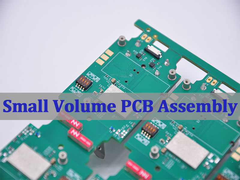
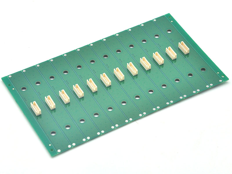
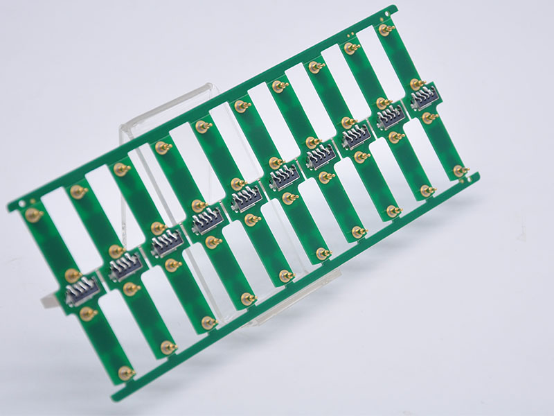
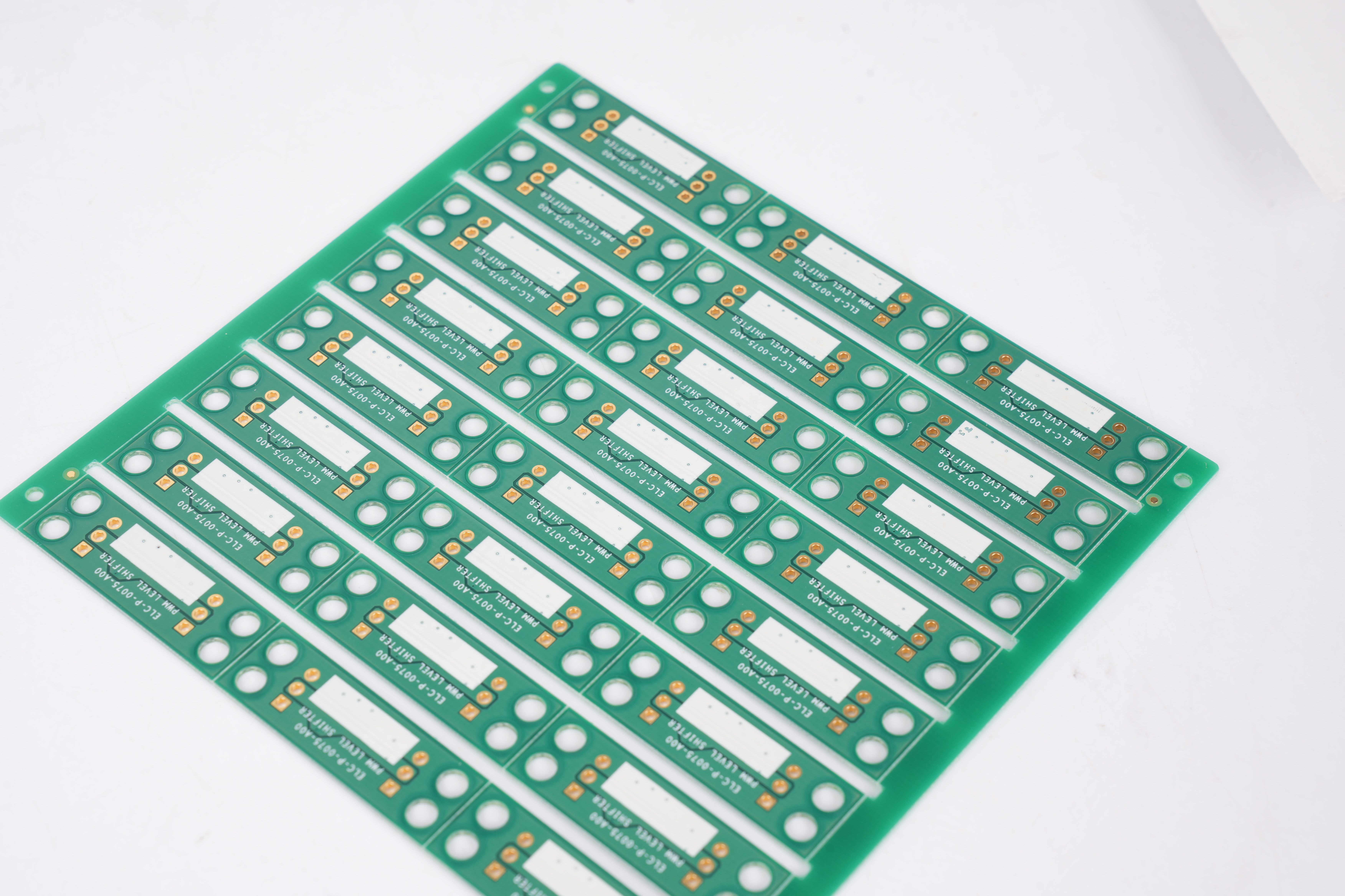
Small volume PCB assembly refers to PCB assembly runs produced in limited quantities—typically ranging from a few boards to several hundred units—primarily used for prototyping, engineering validation, pilot runs, and early market introduction. Unlike mass production, the goal of small volume PCB assembly is not cost minimization, but risk control, design verification, and manufacturability validation.
Have you ever experienced early PCB builds that looked fine on paper but failed once assembled?
Common challenges engineers face in small volume PCB assembly include:
Assembly issues appearing only after the first physical build
Frequent BOM or design changes disrupting production flow
High per-unit cost without clear cost drivers
Long lead times caused by poor coordination
Difficulty transitioning prototypes into stable production
Corresponding manufacturing solutions include:
Engineering-led DFM review before assembly
Flexible process planning for frequent revisions
Transparent cost structure focused on setup and risk drivers
Dedicated project coordination for small batches
Scalable process design aligned with future volume builds
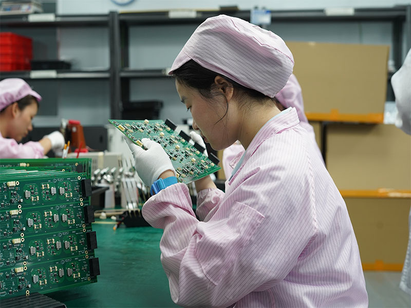
As an established PCB and PCBA manufacturer, EBest Circuit (Best Technology) supports customers from early prototypes to volume production. Our engineers, customer managers, and sales teams know the ropes, combining professional training with hands-on manufacturing expertise. Rather than getting caught up in a rat race of price competition, we prioritize engineering value and long-term collaboration. Our no-MOQ policy is designed to support small-volume PCBA builds, enabling faster validation and smoother scaling. Having partnered with leading brands across the United States, Germany, Israel, and Australia for nearly two decades, we bring proven, real-world PCBA solution experience to every project. For more information or to submit an inquiry, please use the contact form on our Contact page.
What Is Small Volume PCB Assembly and When Is It Required?
Small volume PCB assembly is typically applied during development stages where designs are still evolving and production risks must be identified early. Quantities usually range from single-digit prototypes to a few hundred boards, depending on project maturity.
From an engineering perspective, this phase is where most hidden issues surface. Footprint tolerances, solder joint behavior, component availability, and thermal performance often behave differently in real builds than in simulation.
In real manufacturing environments, small volume PCB assembly is commonly required for:
Engineering validation (EVT) to confirm circuit functionality
Design validation (DVT) to verify assembly feasibility
Process validation (PVT) to assess yield stability
Compliance and certification testing
Pilot runs before market launch
Project Stage
Why Small Volume Assembly Is Used
EVT
Detect schematic and layout flaws
DVT
Validate assembly consistency
PVT
Stabilize yield before scale
Pilot
Limit risk exposure
From an engineering standpoint, recognizing these stages early prevents costly redesigns later.
How Does PCB Assembly Small Volume Differ From Mass Production?
PCB assembly small volume differs fundamentally from mass production in both priorities and execution. While mass production focuses on throughput and unit cost, small volume assembly prioritizes flexibility, inspection depth, and engineering feedback.
In practice, small volume builds often involve manual or semi-automated steps, frequent setup changes, and closer human oversight. This allows engineers to observe problems directly instead of relying solely on statistical process control.
Key differences include:
Higher engineering involvement per build
Frequent BOM and design revisions
More intensive inspection and documentation
Lower automation dependency
Shorter feedback loops
In practice, treating small volume builds like mass production often leads to missed risks and rework.
Why Do Engineers Choose Small Volume PCB Assembly for Early Builds?
Engineers choose small volume PCB assembly because it allows them to validate assumptions before committing resources. Early builds act as a safety net, exposing real-world behavior that simulations cannot fully predict.
From a practical standpoint, early assembly reveals:
Component fit and orientation issues
Solderability and pad design problems
Thermal and power distribution behavior
Assembly accessibility for test and debug
These insights are difficult—if not impossible—to gain without physical boards.
With this in mind, small volume PCB assembly serves as a decision-making tool rather than a production shortcut.
How Does China PCB Assembly Small Volume Support Rapid Product Validation?
China PCB assembly small volume offers a mature ecosystem that balances speed, engineering expertise, and supply chain access. This makes it well suited for rapid product validation without excessive cost exposure.
In real manufacturing scenarios, advantages include:
Fast component sourcing through established suppliers
Skilled assembly labor experienced with complex designs
These factors allow engineering teams to test, adjust, and retest designs efficiently.
As a result, development timelines can be shortened without sacrificing build quality.
What Engineering Challenges Are Common in Small Volume PCB Assembly?
Despite its flexibility, small volume PCB assembly introduces unique challenges that must be actively managed. These challenges stem from frequent change and limited repetition.
Common issues include:
BOM instability and component substitutions
Incomplete or evolving documentation
Manual process variability
Higher sensitivity to operator skill
If unmanaged, these challenges can distort validation results and delay decision-making.
Under real manufacturing conditions, engineering oversight is essential to keep data meaningful.
How Does Small Volume PCB Assembly Cost Compare Across Build Stages?
Small volume PCB assembly cost is driven less by material quantity and more by setup effort, engineering time, and inspection intensity. Understanding this helps teams budget realistically.
Build Stage
Primary Cost Driver
Prototype
Setup and engineering
Pilot Run
Yield learning
Pre-production
Process optimization
Attempting to force mass-production pricing logic onto small volume builds often leads to hidden costs.
That said, transparent cost models allow smarter scaling decisions.
What Quality Controls Matter Most in Small Volume PCB Assembly?
Quality in small volume PCB assembly depends on discipline rather than automation. With fewer boards, each unit carries more informational value.
Critical quality controls include:
First article inspection (FAI)
AOI and functional testing
Documented rework procedures
Lot-level traceability
These controls ensure early builds generate reliable engineering feedback.
More importantly, consistent quality control protects downstream scalability.
How Can Small Volume PCB Assembly Scale Smoothly Into Production?
Scaling successfully requires aligning early builds with future production requirements. Decisions made during small volume assembly often determine whether scaling is smooth or painful.
Best practices include:
Using production-ready footprints early
Freezing process documentation progressively
Tracking yield trends from the first lot
Aligning supplier choices with volume needs
At this stage, small volume assembly becomes a strategic investment rather than a temporary step.
Why Choose EBest Circuit (Best Technology) for Small Volume PCB Assembly?
EBest Circuit (Best Technology) combines engineering discipline with execution capability to support small volume PCB assembly effectively.
Our strengths include:
A 1+3 technical support model, with three dedicated engineers assigned to each project
Ultimately, we help engineers move from concept to production with confidence.
What it ultimately boils down to is that small volume PCB assembly enables engineers to validate designs, manage risk, and prepare for scalable production. This article explored how small volume assembly works, how costs and quality are controlled, and how it supports product development. EBest Circuit (Best Technology) delivers engineering-led execution, digital traceability, and one-stop PCB/PCBA services to support every stage. A warm welcome to contact us at sales@bestpcbs.com to discuss your small volume PCB assembly project.
FAQ: Small Volume PCB Assembly
Q1: What quantity is considered small volume PCB assembly? Small volume PCB assembly typically ranges from a few units to several hundred boards, depending on complexity and project stage.
Q2: Is small volume PCB assembly suitable for production? Yes. It is often used for pilot runs and early market validation before scaling to mass production.
Q3: Why is DFM important in small volume PCB assembly? DFM identifies layout and assembly risks early, reducing rework and delays during later stages.
Q4: Can small volume PCB assembly transition into volume manufacturing? Yes, when processes and documentation are planned correctly from the start.
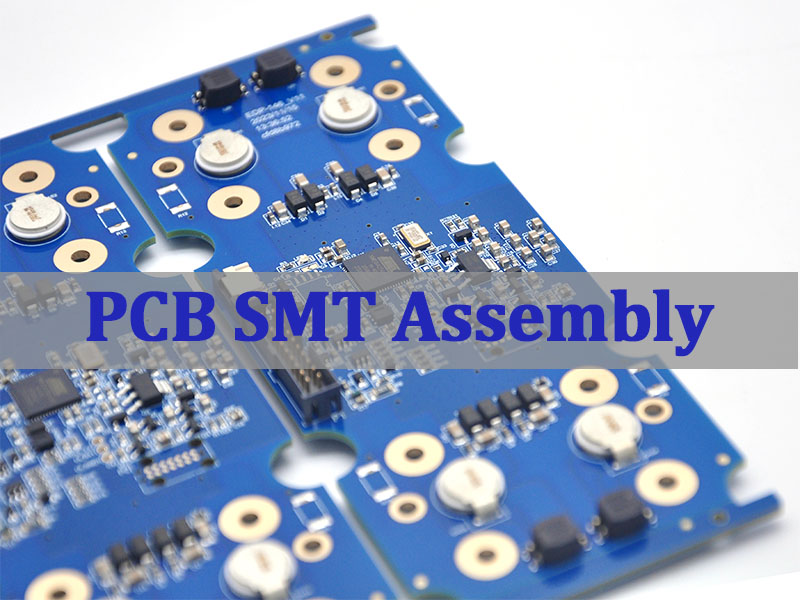
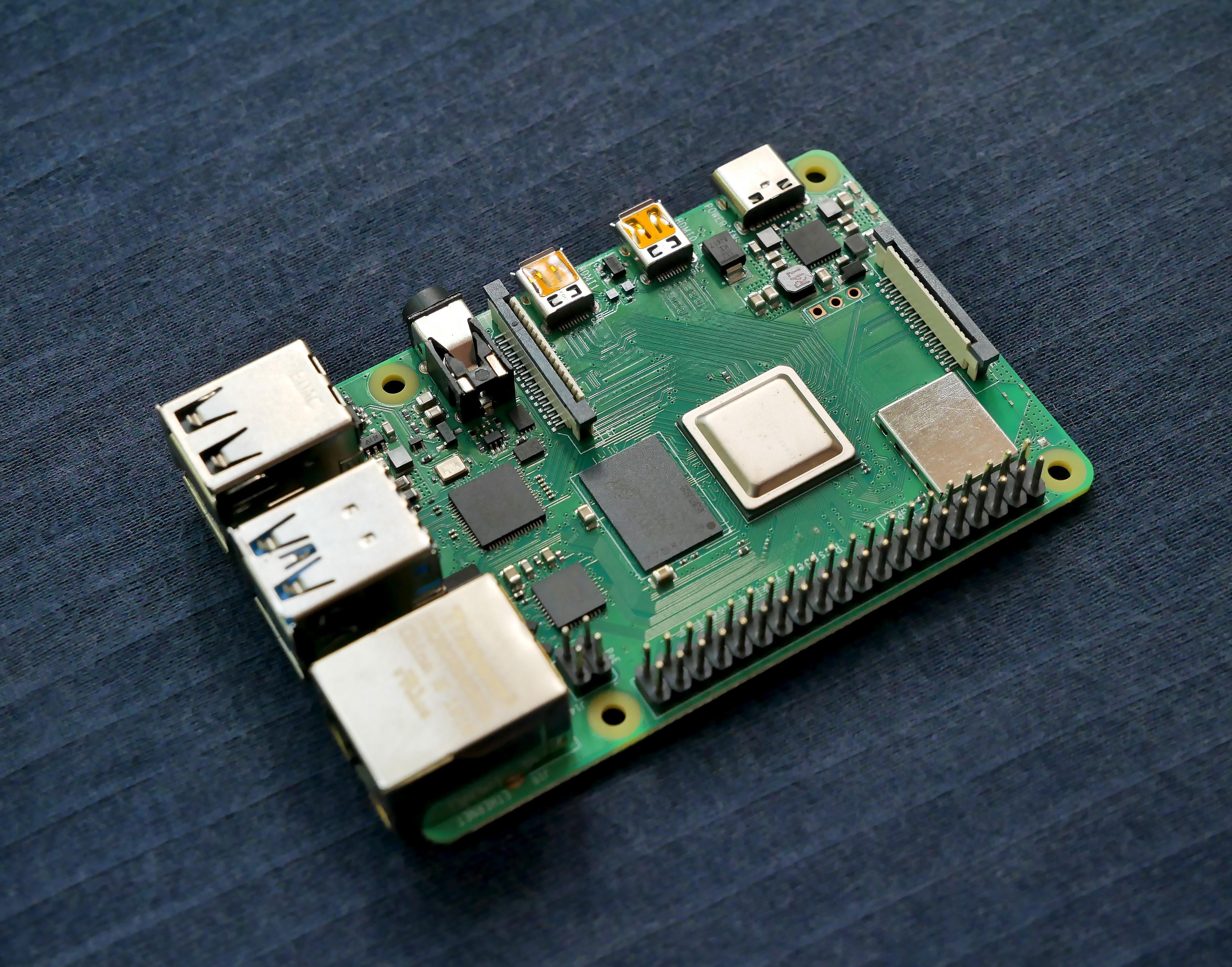
PCB SMT assembly is a highly automated manufacturing method in which surface-mount devices (SMDs) are accurately placed and soldered onto a printed circuit board through controlled reflow processes, enabling high-density circuit layouts, consistent electrical performance, and efficient mass production. This article explains what PCB SMT assembly is, how the process works, what equipment and quality controls are involved, and how engineers can select a reliable SMT assembly partner for prototypes and production.
EBest Circuit (Best Technology) places a high priority on engineering quality, process control, and long-term customer collaboration, supported by strong professional talents across PCB fabrication and SMT assembly. Our technical team includes multiple engineers with over 20 years of hands-on PCB and PCBA experience, and several senior engineers and customer managers who have worked at our company for more than 10 years, ensuring continuity and deep product understanding. As a self-owned factory, every project is supported by a dedicated project coordinator, so customers do not need to worry about production progress or delivery schedules—process visibility and lead-time control are built into our workflow. For project inquiries or technical discussions, pls feel free to contact us directly at sales@bestpcbs.com.
What Is PCB SMT Assembly?
PCB SMT assembly refers to the process of mounting surface-mount devices (SMDs) directly onto the surface of a printed circuit board using automated placement and reflow soldering. It is the backbone of modern electronics manufacturing, enabling compact layouts, higher signal integrity, and scalable production.
From prototype validation to wholesale electronics production, PCB SMT assembly allows engineers to balance performance, manufacturability, and cost. Compared with legacy through-hole methods, SMT supports finer pitch components, double-sided layouts, and high-speed signal routing without sacrificing reliability.
PCB SMT Assembly Process Explained Step by Step
The SMT PCB assembly process is a tightly controlled sequence. Each stage builds on the previous one, and small deviations compound quickly if not engineered upfront.
Prototype vs Wholesale PCB SMT Assembly: Cost and Risk Differences
Item
Prototype SMT PCB Assembly
Wholesale SMT PCB Assembly
Primary goal
Speed and validation
Cost and consistency
BOM flexibility
High
Low
Process tuning
Manual + adaptive
Locked and repeatable
Risk tolerance
Higher
Very low
Trying to apply wholesale pricing logic to prototype projects often leads to rework and schedule overruns.
Common SMT PCB Assembly Defects and How to Prevent Them
Typical SMT assembly defects
Defect Type
Root Cause
Prevention Method
Solder bridging
Excess paste
Stencil aperture tuning
Tombstoning
Thermal imbalance
Pad symmetry control
Insufficient solder
Low paste volume
Printer calibration
BGA voids
Flux entrapment
Profile optimization
Defect prevention always starts at PCB design and SMT assembly guidelines, not at inspection.
Lead-Free and High-Reliability PCB SMT Assembly Standards
Lead-free PCB SMT assembly places significantly higher demands on thermal control and process stability compared with traditional tin-lead soldering, as elevated reflow temperatures reduce the allowable process window and increase stress on both components and PCB materials.
Key engineering implications of lead-free SMT
Higher peak reflow temperatures Lead-free alloys typically require peak temperatures in the 235–250 °C range, increasing the risk of PCB warpage, component cracking, and solder joint fatigue if profiles are not precisely controlled.
Greater sensitivity to PCB material selection PCB laminate Tg, Td, and CTE become critical under lead-free conditions. Inadequate material choices can lead to delamination, pad lifting, or micro-cracking during reflow.
Stronger need for documented process control Lead-free SMT demands tightly defined reflow profiles, verified thermal uniformity, and repeatable machine settings, all supported by controlled work instructions and change management.
For high-reliability PCB SMT assembly, compliance extends beyond soldering itself. These applications require full material and process traceability, validated reflow profiles, and documented inspection criteria such as AOI and X-ray acceptance standards to ensure consistent quality across production batches.
Flex, Rigid-Flex, and Mixed SMT/THT PCB Assembly
Flex PCB SMT assembly
Requires dedicated support fixtures
Lower placement force to avoid deformation
Stress-aware reflow profiles
Mixed board assembly SMT THT PCB
SMT completed first
THT handled via selective soldering
Protects sensitive SMT joints
How to Choose a Reliable PCB SMT Assembly Manufacturer?
Engineers should evaluate capability beyond surface claims.
Transparent quotations clarify trade-offs and avoid surprises during production.
To sum up, PCB SMT assembly is a process-driven manufacturing discipline that directly determines product reliability, yield stability, and time-to-market.
Our strength lies in engineering-led SMT execution (technical team support and DFM pre-review), one-stop PCB manufacturing, component sourcing, and PCBA integration, and fast-turn PCBA delivery with digital traceability. If you need dependable PCB SMT assembly for prototypes or production, pls feel free to contact us via sales@bestpcbs.com.
FAQ: PCB SMT Assembly
Q1: What is SMT in PCB assembly?
SMT in PCB assembly refers to Surface Mount Technology, where electronic components are mounted directly onto the surface of a printed circuit board using automated placement and reflow soldering. This method supports higher component density, smaller board size, and efficient mass production.
Q2:Is SMT PCB assembly suitable for low-volume projects? Yes. Prototype SMT PCB assembly supports fast design verification.
Q3: How reliable is BGA SMT assembly? With X-ray inspection and controlled profiles, BGA reliability is very high.
Q4: What files are required for SMT PCB assembly? Gerbers, BOM, centroid file, assembly drawing, and test requirements.
Q5: Can SMT and THT be combined on one board? Yes. Mixed SMT/THT PCB assembly is common in industrial designs.
Q6: How long does PCB SMT assembly take? Typical lead time is 7–10 working days, depending on sourcing.
Q7: How much does PCB SMT assembly cost?
PCB SMT assembly cost depends on factors such as component count, board complexity, package types (BGA, fine-pitch), inspection requirements, and production volume. Prototype assemblies typically cost more per unit than volume production due to setup and sourcing overhead.
Q8: What equipment is used in SMT assembly?
SMT assembly uses solder paste printers, pick-and-place machines, reflow ovens, AOI systems, and X-ray inspection equipment. These machines work together to ensure placement accuracy, solder joint quality, and process consistency.
Q9: What is the difference between PCB fabrication and SMT assembly?
PCB fabrication focuses on manufacturing the bare circuit board, while SMT assembly involves mounting and soldering electronic components onto the finished PCB. Both processes are essential but occur at different stages of electronics production.
Q10: What are the limitations of SMT in PCB assembly?
SMT is less suitable for very large or high-power components that require strong mechanical support. It also demands tighter process control and higher upfront equipment investment compared to traditional through-hole assembly.
Circuit board vs motherboard is a common comparison, but the two terms are not interchangeable. A circuit board is the basic platform that holds and connects electronic components using copper traces. It is used in almost every electronic product, from simple controllers to complex industrial equipment.
What is a Circuit Board?
Circuit board is the physical platform that supports and connects electronic components. It provides mechanical stability, electrical pathways, and thermal management for an electronic system. Copper traces etched or printed onto an insulating base material form the conductive routes that allow current and signals to flow between components.
Circuit board is not a finished product by itself. It is a foundation. Components such as resistors, capacitors, integrated circuits, and connectors are mounted onto the board through surface-mount or through-hole methods. Once assembled, the board becomes a functional electronic unit.
In practical manufacturing terms, a PCB board serves several purposes at the same time. It ensures reliable electrical connections, keeps component placement organized, and improves consistency in mass production.
From consumer electronics to industrial automation, circuit boards are everywhere. You will find them inside power supplies, LED lighting, medical monitors, automotive controllers, and communication equipment.
At EBest Circuit (Best Technology), circuit boards range from basic two-layer boards to advanced HDI structures. Each design is tailored to its electrical load, signal speed, and operating environment.
What are the different types of circuit boards?
Circuit boards are not all built the same way. Their structure, material, and complexity vary based on application needs.
Common types of circuit boards include:
Single-layer circuit boards: These boards have copper on only one side. They are simple, low cost, and widely used in basic electronics such as toys, adapters, and simple control modules.
Double-layer circuit boards: Copper exists on both sides of the substrate. Vias connect the two layers. This design allows higher component density and more routing flexibility.
Multilayer circuit boards: These boards contain three or more copper layers stacked with insulating material in between. They support complex routing, controlled impedance, and stable power distribution.
Rigid circuit boards: Made from materials like FR-4, rigid boards hold their shape. They dominate most electronics applications.
Flexible circuit boards: Built on polyimide films, these boards bend and fold. They are common in cameras, wearables, and compact consumer devices.
Rigid-flex circuit boards: A hybrid of rigid and flexible sections. They reduce connectors and improve reliability in space-constrained designs.
Each of these is still a circuit board. A motherboard belongs to this family, but with a very specific role and structure. EBest Circuit (Best Technology) manufactures all of these PCB board types, adjusting stack-ups, copper thickness, and surface finishes to match functional demands.
What is a Motherboard?
Motherboard is a specialized and highly integrated type of circuit board. Its primary function is to act as the central connection hub of an electronic system. Unlike simpler PCB boards that serve one function, a motherboard coordinates multiple subsystems at once.
In a computer or embedded system, the motherboard hosts the main processor, memory interfaces, power regulation circuits, and communication buses. It allows different modules to talk to each other through well-defined electrical pathways.
The term “motherboard” originated in computing, but today it extends beyond desktop PCs. Industrial controllers, medical devices, networking equipment, and even automotive control units can have motherboard-style PCBs. In these cases, the board may not resemble a PC motherboard visually, but the architectural role is similar.
Motherboards usually demand tighter tolerances, higher layer counts, and stricter signal integrity control. Power delivery and grounding must be carefully planned. Small layout mistakes can cause noise, instability, or overheating.
EBest Circuit (Best Technology) often supports customers who move from simple PCB boards to full motherboard designs as their products mature. This transition requires deeper engineering coordination and manufacturing discipline, especially for multilayer stack-ups and high-speed signals.
What are the different types of Motherboards?
Just as circuit boards come in many forms, motherboards also vary by application and scale.
Typical motherboard types include:
Desktop computer motherboards: These boards support CPUs, RAM slots, graphics cards, storage interfaces, and peripheral connectors.
Server motherboards: Designed for reliability and continuous operation. They support multiple processors, large memory capacity, and advanced power management.
Embedded system motherboards: Used in industrial machines, medical devices, and automation systems. They focus on stability, long lifecycle, and specific I/O requirements.
Industrial control motherboards: These boards operate in harsh environments. They may include reinforced power circuits, wider temperature tolerance, and thicker copper layers.
In all cases, the motherboard PCB layers are carefully engineered to balance signal routing, power planes, and thermal paths. EBest Circuit (Best Technology) frequently works on custom motherboard PCB projects where off-the-shelf solutions do not meet performance or size requirements.
Is the motherboard the same as the circuit board?
The short answer is no, they are not the same, but they are closely related.
A motherboard is a circuit board, but not every circuit board is a motherboard. The distinction is functional rather than material. A circuit board can perform a single task, such as voltage regulation or signal conversion. A motherboard integrates many tasks and coordinates system-level operation.
Think of a circuit board as a component, and a motherboard as a system platform. The motherboard often contains or connects to multiple other PCB boards. These may include daughter boards, expansion cards, or functional modules.
What is the difference between motherboard and circuit board?
From a design standpoint, a circuit board usually focuses on one function. It may amplify a signal, convert power, or control a motor. A motherboard must support many functions at once and ensure they work together without interference.
From a structural standpoint, motherboards often require more layers. High-speed data lines, stable power planes, and controlled impedance routing are common. A simple PCB board may only need one or two layers.
From a manufacturing standpoint, motherboard production involves tighter inspection standards. Layer alignment, impedance testing, and thermal reliability become critical. At EBest Circuit (Best Technology), motherboard PCB projects often go through additional design-for-manufacturing checks before fabrication begins.
Another practical difference lies in lifecycle expectations. Motherboards are expected to last longer and support firmware updates or hardware revisions. Circuit boards used as submodules may be replaced or redesigned more frequently.
How does PCB motherboard design work?
PCB motherboard design is a structured and disciplined process. It starts with system architecture rather than component placement.
The design process typically includes several coordinated steps. Engineers first define functional blocks and interfaces. They then allocate PCB motherboard layers for power, ground, and signals.
Component placement follows strict rules. Processors, memory, and power circuits are positioned to minimize noise and heat. Decoupling capacitors are placed close to critical pins.
Once routing is complete, simulation and verification take place. Signal integrity, power integrity, and thermal behavior are analyzed.
EBest Circuit (Best Technology) supports this process by providing early feedback on stack-up feasibility, copper weight selection, and drilling limits. This collaboration reduces rework and speeds up time to production.
How many motherboard PCB layers are there?
The number of motherboard PCB layers varies widely based on application complexity. There is no fixed standard, but trends are clear across industries.
Entry-level embedded motherboards may use four layers. This configuration allows basic separation of power, ground, and signals. It suits moderate-speed designs with limited interfaces.
More advanced systems often use six to eight layers. These additional layers improve signal routing freedom and noise control. Industrial and communication products commonly fall into this range.
High-performance motherboards, such as those used in servers or advanced computing, may use ten layers or more. These designs support dense routing, multiple power domains, and high-speed buses.
At EBest Circuit (Best Technology), multilayer PCB capabilities support a wide range of motherboard PCB layer counts. Stack-ups are customized to balance cost, performance, and manufacturability.
Conclusion:
The comparison of circuit board vs motherboard becomes straightforward once roles are clearly defined. A circuit board is the foundation of electronic connectivity, while a motherboard is a specialized circuit board that coordinates an entire system. Every motherboard is a printed circuit board, but only a small portion of PCB boards qualify as motherboards.
Whether you are building a single-function PCB board or a full system motherboard, professional guidance makes a measurable difference.
For technical consultation, PCB fabrication, or PCBA services, you can contact the EBest Circuit (Best Technology) team directly at sales@bestpcbs.com
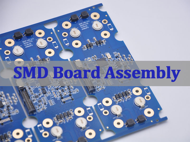
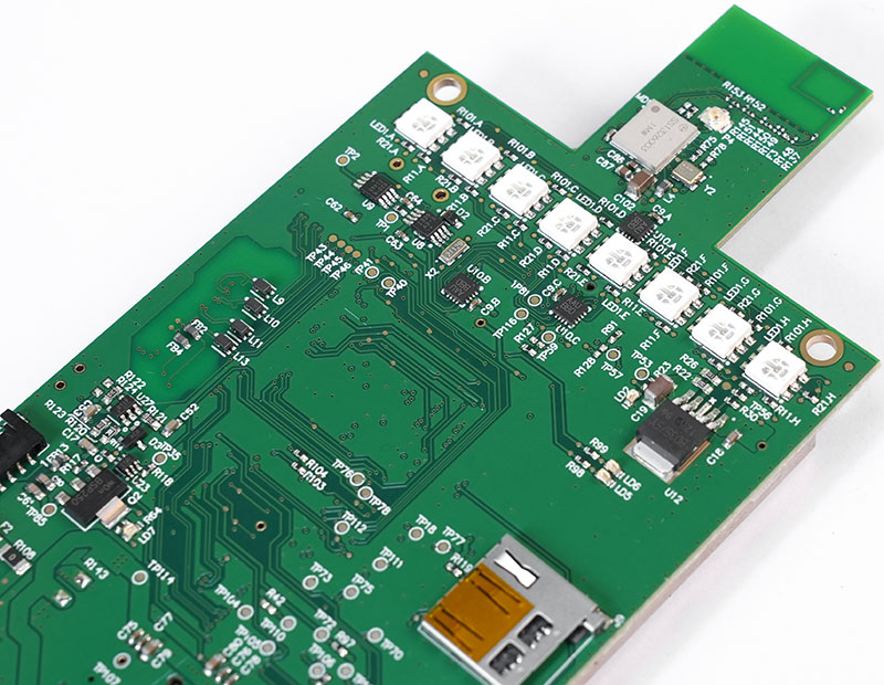
SMD board assembly is the most widely used method for building compact, high-density electronic products today, especially in applications where space utilization, electrical performance, and production efficiency must be tightly controlled. In real production environments, SMD board assembly directly determines electrical reliability, thermal behavior, signal integrity, and long-term field performance, rather than just visual assembly quality.
This article explains how SMD board assembly works in real manufacturing scenarios, what drives its cost, and how engineers and buyers can select a capable SMD board assembly supplier. If you are sourcing SMD board assembly services for prototypes or volume production, EBest Circuit (Best Technology) provides production-ready solutions backed by stable SMT lines and engineering support. For orders or technical discussion, pls feel free to contact us via sales@bestpcbs.com.
What Is SMD Board Assembly and Where Is It Used?
SMD board assembly is the process of mounting surface-mount electronic components directly onto a printed circuit board using automated SMT equipment and controlled soldering processes. It is the dominant assembly method for modern electronics because it enables high component density, repeatable quality, and scalable production.
Compared to through-hole assembly, SMD assembly allows shorter signal paths, better high-frequency performance, and faster production cycles, making it suitable for both prototypes and mass production.
SMD Board Meaning vs SMT Assembly: Are They the Same?
SMD refers to the components themselves, while SMT describes the manufacturing technology used to place and solder those parts onto the PCB. In practical production environments, SMD board assembly brings these two concepts together as a single, well-defined manufacturing workflow. From an engineering perspective, the distinction matters less than the consistency and control of the assembly process.
The key distinction is straightforward:
SMD (Surface-Mount Device): the component itself, such as resistors, capacitors, ICs, and LEDs
SMT (Surface-Mount Technology): the assembly process, including solder paste printing, component placement, and reflow soldering
In real-world manufacturing, “SMD board assembly” and “SMT board assembly” describe the same production workflow from an engineering and procurement perspective. SMD PCB assembly board and SMT PCB assembly board refer to the same type of assembled PCB. SMD describes the component type, while SMT describes the assembly process. In practical manufacturing, both terms are used interchangeably.
How Does SMD Board Assembly Work Step by Step?
board assembly SMT SMD follows a controlled and repeatable sequence designed to minimize defects and ensure consistent solder joint quality. Each step is critical and cannot be treated independently.
A standard SMD assembly flow includes:
Solder paste printing to define solder volume and joint geometry
SPI inspection to verify paste height, area, and alignment
Pick-and-place of SMD components using automated placement machines
Reflow soldering with a controlled thermal profile
AOI inspection to detect placement and solder defects
Functional testing to confirm electrical performance
Small deviations at early stages often lead to yield loss later, which is why process control matters more than visual inspection alone.
What Components Are Used in SMD Board Assembly?
SMD electronic components are standardized by package size and mounting style, which allows automation and high placement accuracy. Component selection directly affects assembly yield, thermal reliability, and rework difficulty.
Common components used in board assembly SMD include:
Chip resistors and capacitors (0402, 0603, 0805, and smaller)
From an assembly standpoint, pad design, package type, and moisture sensitivity must be considered together rather than independently.
SMD Board Assembly for LED and Power Applications
LED and power-related boards place higher demands on SMD board assembly due to thermal and electrical stress. In these applications, solder joints are part of the thermal path, not just electrical connections.
Key assembly considerations include:
Thicker copper PCBs to improve current carrying and heat spreading
Precisely controlled reflow profiles to avoid LED damage
Void control on thermal pads to reduce junction temperature
Optical, electrical, and aging tests after assembly
Poor assembly control in LED boards often results in early measuring drift or premature failure, even when components are qualified.
SMD Prototype Board vs Mass Production Assembly
SMD prototype assembly prioritizes speed and design verification, while mass production emphasizes consistency, yield, and cost optimization. Understanding the difference helps avoid redesigns later.
Production assembly: automated inspection, stable BOM sourcing, process locking
Designing footprints and layouts with production constraints in mind significantly reduces future revisions and ramp-up risks.
What Equipment Is Required for SMD PCB Assembly?
Professional PCB board SMD SMT assembly relies on a complete set of automated equipment rather than isolated machines. The overall line capability matters more than any single piece of equipment.
Core equipment typically includes:
Automatic solder paste printers
High-speed and high-accuracy pick-and-place machines
Multi-zone reflow ovens
AOI and X-ray inspection systems
Equipment accuracy and maintenance level directly influence defect rates, especially for fine-pitch and high-density boards.
SMD Board Assembly Machine and Cost Factors
SMD board assembly machines determine placement accuracy, throughput, and achievable defect levels. More advanced machines reduce long-term cost by improving yield.
Key cost drivers include:
Total component count per board
Presence of fine-pitch or BGA devices
Single-sided vs double-sided assembly
Inspection depth and test coverage
Higher automation usually increases setup cost but lowers per-unit cost in stable production.
China SMD Board Assembly: Quality and Risk Control
China remains the global center for SMD board assembly due to its mature supply chain and manufacturing infrastructure. However, quality is determined by process control, not location.
Reliable SMD assembly factories typically provide:
Structured supplier audits and pilot builds are effective ways to control sourcing risk.
How Much Does SMD Board Assembly Cost? (Price Reference)
SMD board assembly pricing is based on structure and complexity rather than a single flat rate. Understanding the pricing logic helps prevent hidden costs.
Actual pricing depends on board size, layer count, component mix, and inspection requirements.
How to Choose a Reliable SMD Board Assembly Manufacturer?
Choosing an SMD board assembly manufacturer should be an engineering decision, not a marketing one. Capability alignment matters more than advertised capacity.
A practical evaluation checklist includes:
SMT line configuration and accuracy
Inspection and testing coverage
Engineering response speed
Quotation transparency
Track record in similar products
A capable SMD board assembly supplier reduces long-term cost by preventing quality escapes and rework.
All in all, this article outlined how SMD board assembly is executed in real manufacturing environments, how cost and quality are managed, and how engineers can evaluate suppliers for both prototype and volume production.
EBest Circuit (Best Technology) provides a one-stop integrated service covering PCB fabrication, component sourcing, PCBA assembly, and testing, while supporting prototypes and small-batch builds to help engineers validate designs and accelerate product launch. With ISO 9001 / ISO 13485 / IATF 16949 / AS9100D certifications, in-house PCB and PCBA factories, and a digital workshop enabling full material and production traceability within seconds, we ensure consistent quality and reliable lead times. If you are planning an SMD board assembly project or need technical consultation, please feel free to contact EBest Circuit (Best Technology) at sales@bestpcbs.com.
FAQ: Common SMD Board Assembly Questions
Q1: Is SMD board assembly suitable for prototypes? Yes. With proper setup and engineering support, it enables fast iteration and low-volume builds.
Q2: What files are required to start SMD PCB assembly? Gerber files, BOM, pick-and-place data, and assembly notes are required.
Q3: Can SMD and through-hole components be combined? Yes. Mixed assembly is common in industrial and power boards.
Q4: What causes most SMD assembly defects? Incorrect solder paste volume, poor footprint design, and uncontrolled reflow profiles.
Q5: How long does SMD board assembly take? Prototypes typically take 3–5 days, while volume production takes 7–15 days.
RS485 is one of the most enduring and widely adopted communication standards in industrial electronics. Despite the rise of Ethernet, wireless communication, and Industrial IoT protocols, RS485 continues to play a critical role in factories, building automation, energy systems, and embedded control applications.
Why has RS485 stood the test of time? The answer lies in its long-distance capability, high noise immunity, multi-device support, and cost-effectiveness. For engineers, system integrators, and OEMs, RS485 remains a dependable solution when reliability matters more than raw bandwidth.
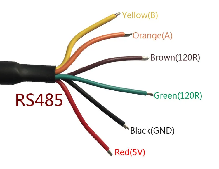
What is RS485 Cable?
An RS485 cable is a balanced, twisted-pair transmission medium that carries differential signals between devices. Instead of referencing voltage to ground, RS485 receivers interpret the voltage difference between two signal lines, which dramatically improves noise immunity.
In practical installations, RS485 cables usually consist of:
One twisted pair for differential data (A/B or D+/D−)
Optional signal ground conductor
Optional foil or braided shield
The twisting ensures that external electromagnetic interference couples equally into both conductors, allowing the receiver to cancel common-mode noise.
In industrial cabinets, shielded RS485 cable is preferred to suppress interference from VFDs, relays, and switching power supplies.
Is RS485 Still Used?
Yes. RS485 is still widely used, and in many industries, it is intentionally preferred.
Despite the rise of Ethernet and wireless communication, RS485 remains common because it solves problems that newer interfaces do not prioritize. These include:
Reliable communication over hundreds or thousands of meters
Operation in high-EMI environments
Simple wiring without switches or hubs
Deterministic behavior for control systems
In factories, substations, and infrastructure projects, predictability and noise tolerance matter more than raw bandwidth. RS485 continues to meet these requirements effectively.
RS485 Cable Specification
A stable RS485 network depends heavily on cable characteristics. Typical RS485 cable specifications include:
Parameter
RS485 Specification
Standard
TIA-485-A (RS-485)
Signaling Type
Differential (Balanced)
Number of Wires
2-wire (half-duplex) or 4-wire (full-duplex)
Conductor Type
Twisted pair
Characteristic Impedance
120 Ω (typical)
Maximum Cable Length
1200 m (4000 ft)
Maximum Data Rate
Up to 10 Mbps
Differential Voltage
≥ ±1.5 V
Receiver Sensitivity
±200 mV
Common-Mode Voltage Range
−7 V to +12 V
Maximum Nodes
32 (standard)
Topology
Linear bus (daisy chain)
Termination Resistor
120 Ω at both ends
Cable Shielding
Optional (Recommended in industrial use)
Ground Reference
Optional but recommended
Connector Types
Screw terminal, DB9, RJ45
Supported Protocols
Modbus RTU, BACnet MS/TP, DMX512
Noise Immunity
High
Typical Cable Type
STP twisted pair, Cat5/Cat6
Is RS485 2-wire or 4 wire?
RS485 supports both 2-wire and 4-wire configurations.
2-wire RS485 (half-duplex)
One twisted pair for transmit and receive
Most common in multi-drop networks
Requires direction control
4-wire RS485 (full-duplex)
Separate pairs for transmit and receive
Allows simultaneous communication
Typically used in point-to-point links
Most industrial RS485 networks use 2-wire topology due to simpler cabling and easier expansion.
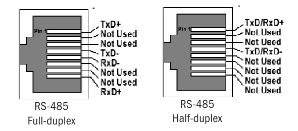
RS485 Pinout
There is no universal RS485 pinout, as RS485 defines electrical signaling—not connectors.
However, common conventions include:
Signal
Description
A (D+)
Non-inverting line
B (D-)
Inverting line
GND
Signal reference (optional but recommended)
Typical pin assignments may be found on:
Terminal blocks
DB9 connectors
RJ45 connectors (vendor-specific)
A frequent source of commissioning failure is A/B polarity reversal, especially when vendors label signals inconsistently. Always verify with a scope or by swapping lines during testing.
⚠️ Important: Some manufacturers label A and B oppositely. Always verify the device datasheet before wiring.
Is RS485 the Same as Ethernet?
No. RS485 is not the same as Ethernet, although RJ45 connectors are sometimes used for RS485.
Feature
RS485
Ethernet
Communication type
Serial
Packet-based
Topology
Bus
Star
Distance
Up to 1200 m
100 m (copper)
Speed
Up to 10 Mbps
100 Mbps – 10 Gbps
Protocol stack
Simple
Complex (TCP/IP)
RS485 focuses on reliability and simplicity, while Ethernet focuses on speed and networking flexibility.
What Type of Cable to Use for RS485?
Recommended RS485 cable characteristics:
Twisted pair (mandatory)
120 Ω impedance
Shielded (STP) for noisy environments
Low capacitance for longer distances
Common choices:
Belden 9841 / 9842
CAT5e (short runs, low noise only)
Industrial RS485-rated cables
What is RS485 Used For?
RS485 is commonly used in applications that require:
Long cable runs
Multiple devices on one bus
Reliable communication under electrical noise
Typical use cases include:
PLC and industrial controllers
Modbus RTU networks
Energy meters and power systems
Building automation and HVAC
Access control and alarm systems
These systems value stability and predictability over raw data speed.
How Do I Connect My RS-485 to My Computer?
Most computers do not have native RS485 ports. Common connection methods include:
USB to RS485 converter (most popular)
PCI/PCIe RS485 expansion card
RS232 to RS485 converter
After connecting, configure:
Baud rate
Data bits
Parity
Stop bits
to match the RS485 device settings.
Does RS-485 Need to Be Grounded?
RS485 does not strictly require grounding, but grounding is strongly recommended for stability and protection.
Best practices:
Connect signal ground between devices
Use shielded cable
Ground the shield at one end only
Avoid ground loops
Proper grounding improves noise immunity and prevents communication errors.
How to Quickly Prove Whether RS485 is Working?
When troubleshooting RS485, follow a structured process:
Confirm correct A/B polarity
Check termination resistors at both ends of the bus
Verify biasing resistors are present
Inspect grounding and shield connections
Reduce baud rate to increase noise margin
Observe waveforms with an oscilloscope if available
Most RS485 issues originate at the physical layer, not the protocol level.
RS485 vs RJ45: What are Differences?
RS485 and RJ45 are frequently confused, especially in industrial projects where RS485 signals are often routed through RJ45 connectors.
However, they represent two completely different layers of a communication system, and understanding this distinction is critical to avoid wiring errors, equipment damage, or unstable communication.
1. Standard definition
RS485 is an electrical signaling standard (TIA-485). It defines:
Differential voltage levels
Driver and receiver characteristics
Noise immunity behavior
Multi-drop bus capability
RS485 says nothing about connectors, pin counts, or cable jackets.
RJ45 is a connector specification. It defines:
8 physical pins
Mechanical dimensions
Contact layout
RJ45 does not define voltage levels, signaling methods, or communication protocols.
This is the root cause of confusion: RJ45 can carry RS485, Ethernet, CAN, or proprietary signals, depending entirely on how the pins are wired.
2. Signal transmission method
This is the most important technical difference.
Aspect
RS485
RJ45
Role
Electrical communication standard
Physical connector
Signal type
Differential (A/B)
None defined
Noise immunity
Very high
Depends on protocol
Defines voltage levels
Yes
No
Defines data format
No
No
RS485 uses differential signaling, which allows it to tolerate high EMI, long cable runs, and ground noise. RJ45 itself provides no electrical noise protection; it simply holds contacts in place.
3. Cable usage and common misconceptions
A major source of misunderstanding is the use of Ethernet cable with RS485.
Many systems run RS485 over:
Cat5 / Cat5e / Cat6 cable
RJ45 connectors
This does not make the system Ethernet.
Why it works:
Ethernet cable contains twisted pairs
Twisted pairs suit RS485 differential signaling well
100 Ω Ethernet cable impedance is close to RS485’s typical 120 Ω requirement
Why problems still occur:
Pinouts are not standardized
Shielding and grounding may differ
Termination and biasing are often ignored
Using an RJ45 connector does not change the fact that the system is still RS485 electrically.
4. Topology differences
RS485 topology
Bus (daisy-chain)
Termination at both physical ends
Limited stub lengths
Multi-drop without switches
RJ45-based Ethernet topology
Star topology
Uses switches and routers
Each device has a dedicated link
This difference matters because star wiring works for Ethernet but often breaks RS485. Engineers accustomed to Ethernet wiring sometimes unknowingly apply the same topology to RS485, leading to reflections and unstable communication.
5. Distance and speed comparison
Parameter
RS485
RJ45 (Ethernet typical)
Typical distance
Up to ~1200 m (speed-dependent)
100 m per segment
Typical speed
kbps to low Mbps
100 Mbps – 10 Gbps
Noise tolerance
Excellent
Moderate
Infrastructure
Simple
Requires switches
Confusing the two leads to incorrect assumptions about topology, grounding, termination, and compatibility. Once the distinction is clear, RS485 systems become far easier to design, troubleshoot, and maintain.
The SMT PCBA process is the backbone of modern electronics manufacturing, involving the automated placement and soldering of components onto printed circuit boards. This article provides a comprehensive guide to building a stable SMT production line, with a special focus on the critical engineering controls needed for turnkey medical device projects.
Launching a medical device often stalls not at design, but at manufacturing—where compliance, reliability, and execution risks quickly compound.
Lack of true medical compliance expertise beyond basic PCB assembly (ISO 13485, FDA QSR).
Unstable sourcing for long-lifecycle medical components and obsolescence risk.
Yield loss and inconsistency when assembling fine-pitch and miniature components.
Heavy documentation and validation burdens for regulatory submissions.
Fragmented communication in turnkey projects without clear ownership.
These challenges are addressed by partnering with a medical-focused EMS provider built around process control, traceability, and regulatory readiness.
ISO 13485–certified quality system with audit-ready workflows and DHF support.
Proactive component lifecycle management through dedicated medical sourcing teams.
Precision SMT lines validated for micro-assembly, supported by AOI and AXI.
Complete IQ/OQ/PQ, PFMEA, and CPK deliverables included as standard.
Dedicated project engineers providing end-to-end ownership from PCBA to box-build.
At EBest Circuit (Best Technology), we are a specialized provider of turnkey PCBA manufacturing services for the medical industry. Our core strength lies in a deeply engineered SMT PCBA process built on precision equipment, statistically controlled workflows, and a quality-first culture. Our SMT production capability is defined by advanced pick-and-place platforms, tightly controlled process flows, and rigorously validated engineering parameters—ensuring every assembly stage meets the stability and repeatability required for medical-grade manufacturing. For a consultation on your next project, contact our team at sales@bestpcbs.com.
What Is The SMT PCBA Process?
The SMT PCBA process refers to the sequence of operations used to populate a bare PCB with electronic components using Surface Mount Technology (SMT). It is the dominant method for high-density, high-volume electronics assembly, including critical medical devices. This process involves applying solder paste, precisely placing components, and using controlled heat to form permanent solder joints. A well-controlled SMT process flow is characterized by repeatability, high yield, and the ability to handle increasingly miniaturized components. For a reliable turnkey medical project, understanding and controlling this process is non-negotiable.
The SMT assembly sequence is commonly broken into three major phases:
Pre-Assembly: This includes all preparatory steps: solder paste printing (stencil application), adhesive dispensing (if needed for mixed-technology boards), and the critical setup and programming of the SMT pick and place machine.
Assembly: The core phase where components are placed onto the pasted PCB. This stage is defined by the speed and accuracy of the automated placement equipment.
Post-Assembly: This encompasses the soldering process (typically reflow soldering), cleaning (for no-clean or water-soluble pastes), and a series of inspections (Automated Optical Inspection – AOI, X-ray Inspection – AXI) to verify quality before any PCBA plug-in assembly of through-hole parts.
In summary, the SMT PCBA process is a sophisticated, phased manufacturing methodology that transforms a bare board into a functional assembly. Its effectiveness directly determines the performance, reliability, and longevity of the final electronic product, especially in life-critical medical applications.
SMT PCBA Process Step By Step Explained
A reliable SMT assembly follows a defined sequence where each step builds upon the quality of the previous one. For medical projects, consistency at every stage is paramount. Here is a detailed breakdown of a standard SMT PCBA process step by step:
Solder Paste Printing: A stainless steel stencil is aligned over the PCB, and solder paste is deposited onto the solder pads. The quality of this print, including volume, alignment, and definition, is the first critical determinant of soldering success.
Solder Paste Inspection (SPI): An inline 3D SPI system measures the height, volume, and area of each solder paste deposit. This real-time feedback allows for immediate correction of printing defects, preventing a cascade of failures later.
Component Placement: The PCB moves to the SMT pick and place machine. Components from reels, trays, or tubes are picked up, optically centered, and placed with micron-level accuracy onto their corresponding solder paste deposits.
Reflow Soldering: The populated board travels through a multi-zone reflow oven on a conveyor. A precise thermal profile melts the solder paste, forms intermetallic bonds, and then cools to create solid, reliable electrical and mechanical connections.
Automated Optical Inspection (AOI): Post-reflow, an AOI system uses high-resolution cameras to check for placement errors, missing components, polarity issues, and visible solder joint defects.
X-Ray Inspection (AXI): For medical assemblies with hidden solder joints (e.g., under BGAs or QFNs), AXI is essential. It verifies internal solder ball integrity, voiding percentage, and alignment, which are critical for long-term reliability.
Conformal Coating & Final Assembly: For medical devices requiring protection from moisture and contaminants, a conformal coating may be applied. Finally, any necessary PCBA plug-in assembly of through-hole components is completed.
This step-by-step SMT PCBA process flow, when executed with precision equipment and strict controls, forms the foundation of a manufacturing line capable of producing medical-grade electronics with the required traceability and zero-defect mindset.
How Does The SMT Automation Process Work?
SMT automation is the backbone of modern medical PCBA manufacturing, enabling the speed, placement accuracy, and process repeatability required for regulated devices. Rather than isolated machines, automation links equipment, software, and data into a synchronized production system that minimizes variability and maximizes control.
At the core of this system is the SMT pick and place platform, supported by automated material handling, closed-loop process control, and centralized data management. Together, these elements form a fully integrated SMT production line designed for consistency, traceability, and validation readiness.
Key Elements of SMT Automation
Material Handling Automated loaders and unloaders feed bare boards into the line and remove completed assemblies, enabling continuous, stable operation with minimal manual intervention.
Pick and Place Operations High-speed and high-precision placement heads handle components ranging from 0201 passives to fine-pitch BGAs, using advanced vision systems for fiducial alignment and placement correction.
Process Linking Conveyor systems synchronize printers, SPI, placement machines, reflow ovens, and inspection stations into a single, balanced production flow.
Data Integration A Manufacturing Execution System (MES) tracks each PCB in real time, associating it with feeder setup, stencil ID, reflow profile, and inspection results to form a complete digital record.
Key Automation Technologies in an SMT Line
Technology
Primary Function
Medical Manufacturing Impact
3D SPI
Paste volume verification
Early defect prevention
High-Precision Placers
Accurate micro-component placement
Supports miniaturized designs
Closed-Loop Reflow
Stable thermal control
Consistent solder reliability
AOI / AXI
Automated defect detection
Objective quality evidence
In practice, SMT automation works as a closed-loop, data-driven environment. Inspection results feed back into placement and printing parameters, while MES data enables statistical process control and full traceability. This structure reduces human variability, stabilizes yield, and generates the documentation foundation required for SMT process validation and regulatory compliance in medical device manufacturing.
What Engineering Controls Ensure A Stable SMT Production Line?
For medical SMT PCBA processing, stability is synonymous with safety. Engineering controls are the documented procedures, specifications, and monitoring systems that prevent process drift and ensure every unit meets specification. A stable line is not achieved by chance but through deliberate, scientific control.
Standardized Operating Procedures (SOPs): Every machine operation and manual task, from stencil cleaning to feeder setup, is governed by a detailed SOP. This eliminates variability between operators and shifts.
Preventive Maintenance (PM) Schedules: Strict, calendar-based maintenance is performed on all critical equipment (printers, placers, ovens). This prevents unplanned downtime and ensures machines consistently perform within specification.
Statistical Process Control (SPC): Key parameters are monitored in real-time using control charts. Examples include solder paste volume (from SPI), placement accuracy, and reflow oven temperatures. SPC signals trends before they become defects.
Process Capability Studies (Cp/Cpk): These statistical measures quantify how well a process (e.g., solder paste printing) can meet its specified tolerance limits. A high Cpk (>1.33 is typical, >1.67 for critical characteristics) indicates a stable, capable process.
Comprehensive Traceability: A lot-tracking system records the specific materials (paste lot, component reel), machine programs, and operator for every board or panel. This allows for targeted containment and root cause analysis if an issue arises.
Environmental Controls: Temperature and humidity in the production area are controlled. Solder paste and moisture-sensitive devices (MSDs) are stored and handled according to strict protocols (e.g., IPC/JEDEC J-STD-033).
These engineering controls transform an SMT line from a collection of machines into a predictable, reliable manufacturing system. They are the tangible manifestations of a quality management system like ISO 13485 and are essential for passing audits and ensuring the long-term reliability of medical devices.
What Are Common PCBA Defects In SMT Assembly?
Even with a well-tuned process, defects can occur. Understanding their root causes is the first step to prevention. For ODM SMT PCBA rapid patch processing providers, rapid diagnosis and correction are key. Common defects include:
Solder Bridging (Short): Solder inadvertently connects two adjacent pins or pads. Often caused by excessive solder paste, poor stencil design, or incorrect reflow profile.
Tombstoning: A passive component (like a resistor or capacitor) stands up on one end. Typically caused by unequal solder paste volume or thermal mass on the two pads.
Insufficient Solder (Open): A solder joint lacks sufficient material to form a reliable connection. Can result from poor paste printing, pad contamination, or an incorrect reflow profile.
Component Misalignment: A part is offset or rotated from its intended position. Usually a fault of the pick and place machine’s calibration, vision system, or poor fiducial recognition.
Voiding (in BGA joints): Gas bubbles trapped within a BGA solder ball. While some voiding is acceptable per IPC standards, excessive voids can weaken the joint and impact thermal performance. Often related to paste chemistry or reflow profile.
Cold Solder Joint: A joint that appears dull, grainy, and has not properly fused. Caused by insufficient heat during reflow or contamination.
Root Cause & Corrective Action (RCCA) for Defects:
A stable medical SMT line relies on immediate defect detection (via AOI/AXI) and systematic RCCA. For example, a spike in bridging defects would trigger an investigation of the stencil’s condition, the printer’s settings, and the recent reflow oven profile, ensuring the issue is corrected at its source.
What Is CPK In SMT Manufacturing Process Control?
Cpk (Process Capability Index) is a crucial statistical measure in SMT process control. It quantifies how well a controlled process can consistently produce outputs within the specified tolerance limits. In simple terms, it tells you if your process is centered and precise enough.
The Concept: Every process has natural variation. Cpk compares the spread of this natural variation (process width) to the distance between the specification limits (customer/engineering requirements). A higher Cpk indicates the process is well-centered and has a smaller spread relative to the limits, meaning a lower probability of defects.
Cpk < 1.0: The process spread is too wide and/or not centered. It is incapable of consistently meeting specs. Immediate corrective action is required. (e.g., Solder paste height is too variable).
Cpk ≥ 1.33: The process is considered capable. This is a common industry minimum.
Cpk ≥ 1.67: The process is highly capable and robust. This is the target for critical characteristics in medical SMT PCBA processing, such as solder paste volume or reflow peak temperature.
For a medical device manufacturer, reporting Cpk values for key processes (paste printing, placement accuracy) is a powerful demonstration of a mature, stable, and statistically validated production line. It moves quality assurance from a “check-the-box” inspection to a predictive science.
What Is The PiP Process In SMT Assembly?
PiP (Pin-in-Paste), also known as Paste-in-Hole or Intrusive Reflow, is a hybrid assembly technique that allows through-hole components to be soldered during the SMT reflow process. This simplifies assembly by eliminating a separate wave soldering or manual soldering step, which is valuable for turnkey projects seeking efficiency.
How it works:
The PCB goes through the standard solder paste printing process.
Solder paste is deposited not only on SMD pads but also into the plated through-holes (PTHs) intended for PiP components.
SMT components are placed as usual.
PiP components (typically connectors or larger electromechanical parts with long leads) are inserted into the paste-filled holes. This can be done manually or with automated insertion equipment.
The entire assembly then passes through the reflow oven. The solder paste in the PTHs melts, flows, and creates a fillet, soldering the PiP component in place.
Advantages for Medical PCBA:
Process Simplification: Reduces the number of soldering stages, lowering cost and cycle time.
Improved Reliability: Can create more robust solder joints for heavy components compared to wave soldering.
Design Flexibility: Useful for mixed-technology boards where a few through-hole parts are needed alongside dense SMT.
Considerations:
Successful PiP requires careful design (adequate PTH size, solder paste volume calculation), specialized stencil design, and process validation to ensure complete hole fill and avoid solder voids.
How Is SMT Process Validation Performed In Mass Production?
SMT process validation is a formal, documented procedure that provides high confidence that a specific SMT process will consistently produce a PCBA meeting all predetermined quality and regulatory requirements. For mass production of medical devices, it is a mandatory gate before commercial launch.
The validation follows a structured, three-phase approach often aligned with the Installation Qualification (IQ), Operational Qualification (OQ), and Performance Qualification (PQ) framework.
Installation Qualification (IQ): Verifies that the SMT production line equipment (printer, SPI, placer, oven) is correctly installed according to manufacturer specifications and site requirements. This includes checking utilities, calibrations, and software versions. Documentation: Equipment manuals, calibration certificates, installation checklists.
Operational Qualification (OQ): Demonstrates that the installed equipment can operate consistently within established limits and tolerances under “worst-case” scenarios. This involves running the machines with test programs and challenging conditions.
Example OQ Tests:
Printer: Repeatability of paste volume across multiple prints.
Placer: Accuracy and repeatability of placement using a test board.
Reflow Oven: Verification of thermal profile consistency across all zones and across the conveyor width.
Performance Qualification (PQ): Also known as Process Validation, this is the most critical phase. It proves that the entire, integrated process, using production-intent materials, can consistently produce acceptable product.
A validation lot (typically 3 consecutive production runs) is manufactured.
The entire SMT PCBA process flow is executed under standard operating procedures.
Every unit is subjected to comprehensive inspection and testing (visual, AOI, AXI, functional test).
Data is collected and analyzed to prove the process is stable and capable (using statistical tools like Cpk).
The outcome is a definitive report stating whether the process is validated for mass production.
For a medical device manufacturer, a completed validation package is a cornerstone of the Design History File (DHF) and is essential for regulatory submissions to bodies like the FDA. It is the ultimate proof that the manufacturing process is under control.
In summary, the SMT PCBA process is a complex yet precisely engineered sequence that forms the critical link between electronic design and a reliable, manufacturable medical device. Mastering this process—from the SMT process flow chart to real-time process control with metrics like CPK—is what separates a basic assembler from a qualified medical manufacturing partner.
This article has detailed the steps, controls, and validation frameworks necessary to achieve the reliability demanded by turnkey medical projects. Success hinges on automation, data-driven engineering, and a culture of continuous improvement.
At EBest Circuit (Best Technology), we have built our service around this principle. Our professional ODM SMT PCBA rapid patch processing is supported by a SMT production line equipped with advanced inspection technology and governed by a strict ISO 13485 quality system. We understand that for medical devices, the process isthe product. Pls feel free to contact our engineering team anytime at sales@bestpcbs.com to discuss your project requirements.
FAQs
How Is A PCBA Different From A PCB?
A PCB (Printed Circuit Board) is the bare, unpopulated board—just the laminate, copper traces, and solder mask. A PCBA (Printed Circuit Board Assembly) is the completed, functional board after all electronic components (SMT and/or through-hole) have been soldered onto it. The SMT PCBA process is what transforms a PCB into a PCBA.
What Is The Difference Between PCB And SMT?
This is a common point of confusion. PCB refers to the physical board itself. SMT (Surface Mount Technology) refers to one of the primary methods used to assemble components onto that PCB. SMT is a PCB assembly process, not the board.
How Do SMT Assembly Services Handle Component Availability?
Professional ODM SMT PCBA rapid patch processing partners manage this proactively. They maintain long-term relationships with franchised distributors, use component market analysis tools to forecast shortages, and offer DFM (Design for Manufacturability) reviews early in the design phase to suggest alternates for parts at risk of obsolescence, which is vital for the long lifecycles of medical devices.
What SMT Component Sizes Are Hardest To Assemble?
The greatest challenges come at the extremes of miniaturization: 01005 (0.4mm x 0.2mm) and smaller passive components, and ultra-fine-pitch components (e.g., 0.3mm pitch BGAs or CSPs). These require ultra-high-precision SMT pick and place machines, specialized stencil designs, and exquisite process control to avoid defects like bridging or misplacement.
What Are Typical Turnaround Times For SMT Assembly Services?
Turnaround time depends on project complexity, layer count, component sourcing, and quantity. For a standard prototype run with all parts in stock, rapid patch processing can be as quick as 24-72 hours for SMT assembly. For new medical projects requiring full process validation and regulatory documentation, the initial timeline will be longer to ensure quality, with subsequent production runs following a predictable schedule.
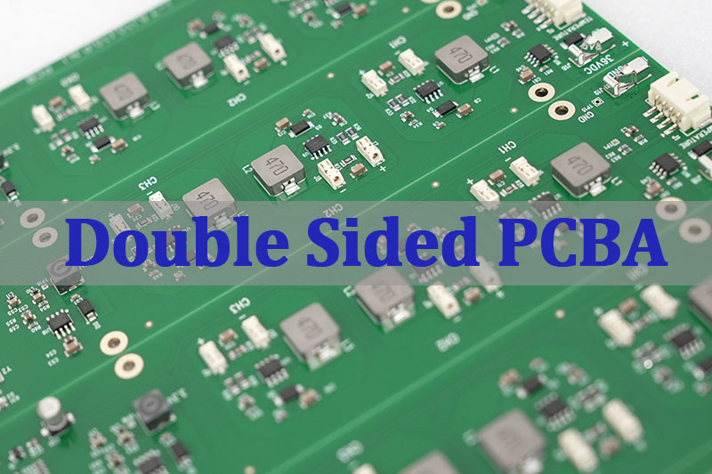
Double sided PCBA refers to a printed circuit board assembly where components are mounted and soldered on both sides of the PCB, enabling higher circuit density and more functional integration within a compact footprint. This article explains how double sided PCBA production works, when it should be selected, what risks commonly occur during assembly, and how an experienced manufacturer controls quality, cost, and delivery across the full production lifecycle.
Why Do Double Sided PCBA Projects So Often Run Into Trouble?
DFM issues are discovered after parts are ordered, forcing rework or redesign.
Double reflow introduces alignment and solder joint reliability risks.
BOM choices look acceptable on paper but fail under real supply constraints.
Quality varies between batches due to inconsistent process control.
Communication gaps slow down prototype-to-production transitions.
A double sided PCBA manufacturer with long-term production experience addresses these risks systematically rather than reactively.
Perform DFM review and process validation before material commitment.
Control double-sided reflow profiles and fixture strategy to stabilize yield.
Optimize BOMs with lifecycle checks and approved alternates.
Apply standardized inspection and quality checkpoints across all builds.
Use clear engineering communication workflows to reduce iteration cycles.
EBest Circuit (Best Technology) is a professional PCB and PCBA manufacturer with over 20 years of double sided PCBA production experience, serving more than 1,800 customers and 10,000 engineers worldwide. With in-house PCB fabrication, PCBA assembly, certified quality systems, and a digitalized production workshop, we help OEM teams move from prototype to volume. For technical consultation or quotations, pls feel free to contact us via sales@bestpcbs.com.
What Does Double Sided PCBA Involve In A Production Assembly Program?
A production-level double sided PCBA program includes more than placing parts on both sides of a board. It is a coordinated manufacturing system.
Key Elements Involved
Engineering Review – DFM, DFA, and process feasibility checks.
PCB Fabrication Alignment – Stack-up, finish, and panelization matched to assembly needs.
Component Preparation – Moisture control, polarity validation, and alternate sourcing.
Double-Sided Assembly – Controlled first-side and second-side reflow sequencing.
Inspection And Testing – AOI, X-Ray (when required), and functional validation.
A structured assembly program ensures that double sided PCBA remains stable and repeatable at production scale.
What Is The Typical Double Sided PCB Manufacturing Process From Design To Assembly?
The manufacturing process must account for thermal, mechanical, and inspection challenges unique to double sided boards.
Typical Process Flow
PCB fabrication with defined copper balance and solder mask design.
Product requires moderate complexity with controlled assembly risk.
To wrap up, double sided PCB design often represents the best balance between functionality and manufacturing cost.
What Are Common Double-Sided PCB Applications In Modern Electronic Products?
Double-sided PCB applications span a wide range of industries where space efficiency and cost control are critical.
Common Applications
Industrial control modules
Power management boards
Consumer electronics
Automotive subassemblies
Communication interface boards
To summarize, double sided PCBA remains a workhorse solution for modern electronics across multiple sectors.
What Factors Affect Quality In China Double Sided PCBA Production?
China double sided PCBA quality depends more on process governance than on geography.
Key Quality Factors
DFM depth and timing
Component sourcing discipline
Reflow profile stability
Inspection coverage and standards
Production traceability
To wrap things up, choosing a China-based manufacturer with mature controls is essential for consistent quality.
What Assembly Risks Are Common In Double Sided PCBA Production?
Double sided PCBA introduces specific risks that must be managed proactively.
Common Assembly Risks
Component shift during second reflow
Tombstoning on small passives
Shadowing effects during AOI
Thermal stress on sensitive devices
Yield loss from inconsistent handling
To sum up, experienced manufacturers mitigate these risks through fixturing, profiling, and inspection strategy.
How Does Double Sided PCBA Compare With Multilayer PCBA In Cost Structure?
From a cost perspective, double sided PCBA often occupies a middle ground between simplicity and complexity.
Cost Structure Comparison
Aspect
Double Sided PCBA
Multilayer PCBA
PCB Cost
Lower
Higher
Assembly Complexity
Moderate
High
Yield Sensitivity
Medium
High
Design Flexibility
Moderate
Very High
In essence, double sided PCBA is often the most cost-effective solution when multilayer routing is not strictly required.
Overall, double sided PCBA enables compact, cost-efficient electronic manufacturing when supported by disciplined engineering and production control. This article reviewed the production scope, manufacturing process, application scenarios, quality factors, assembly risks, and cost structure considerations associated with double sided PCBA.
As a double sided PCBA manufacturer with 20 years of production experience, EBest Circuit (Best Technology) combines engineering depth, certified quality systems, digital traceability, and fast turnaround to help OEMs achieve stable, scalable results. For project evaluation or quotations, pls feel free to contact us via sales@bestpcbs.com.
FAQs
What is the difference between single sided and double sided PCB?
A single sided PCB places components on one side only, while a double sided PCB allows components on both sides, increasing circuit density and routing options.
How are double-sided PCBs assembled?
Double-sided PCBs are assembled through sequential placement and reflow, typically soldering one side first, then flipping the board and assembling the second side with controlled fixturing and thermal profiles.
Through hole vs surface mount are the two main methods for attaching electronic components to a printed circuit board, and each serves different design and manufacturing needs.
What Is the Difference Between SMT and THT?
Through hole technology, often called THT or through hole mount, uses component leads that pass through drilled holes in the PCB. These leads are inserted, soldered on the opposite side, and mechanically anchored by the plated hole wall. This method relies heavily on through hole drilling, copper plating, and solder fillets that form on both sides of the board.
Surface mount technology, or SMT, works very differently. Components are placed directly onto pads on the PCB surface. No lead passes through the board. Instead, solder paste holds the part in place during reflow. This approach supports compact layouts, fine-pitch parts, and high-speed automated placement.
Through hole requires drilling, desmear, and hole plating
SMT focuses on stencil printing, placement accuracy, and reflow profiling
THT boards often need wave soldering or selective soldering
SMT boards rely on reflow soldering and AOI inspection
At EBest Circuit (Best Technology), mixed-technology boards are common. Many designs use surface mount components for logic and control, while keeping through hole components for connectors, transformers, or power devices.
What Are the Disadvantages of SMT?
Surface mount technology delivers speed and density, but it is not without limitations.
One challenge is mechanical strength. Surface mount parts rely entirely on solder joints attached to surface pads. Under heavy vibration or mechanical stress, these joints need proper pad design and solder volume to remain stable.
Thermal handling can also be more demanding. Small surface mount packages dissipate heat through pads and copper planes. Poor thermal design may cause overheating if copper balance or via placement is incorrect.
Another consideration is inspection and rework. Fine-pitch SMT components require magnification, X-ray inspection, and skilled rework processes.
Increased difficulty in manual rework for very small packages
Experienced manufacturers, including EBest Circuit (Best Technology), mitigate these issues through controlled stencil design, profile tuning, and process validation.
What Are the Disadvantages of Through-Hole Soldering?
When reviewing surface mount vs through hole soldering, through hole soldering presents a different set of trade-offs.
The most visible limitation is space. Through hole components occupy both sides of the PCB and require clearance around each drilled hole. This reduces routing density and limits miniaturization.
Manufacturing time is another factor. Through hole soldering often involves manual insertion or slower automated processes. Wave soldering is efficient for large volumes, but setup and fixturing take time.
Cost is also influenced by drilling. Each plated hole adds fabrication steps, tool wear, and inspection effort. For dense designs, through hole drilling increases PCB cost compared to pure SMT layouts.
Despite these points, through hole technology remains valuable. Its disadvantages are mostly related to scale and size, not reliability. For power and structural roles, its benefits often outweigh its limits.
Is Surface Mount Better Than Through-Hole?
Surface mount excels in high-density electronics. It supports smaller boards, faster assembly, and lower per-unit cost at volume. Consumer electronics, IoT devices, and compact control modules rely heavily on SMT for this reason.
Through hole shines where strength and current handling matter. Large electrolytic capacitors, power inductors, relays, and connectors benefit from the mechanical anchor of plated holes.
What Is the Main Advantage of SMT Over Through-Hole Technology?
The main advantage of SMT over through hole technology is efficiency. This efficiency appears in several practical ways.
First, component density increases. Surface mount packages are smaller and do not require holes, allowing more components per square inch.
Second, automation improves consistency. SMT lines place thousands of parts per hour with repeatable accuracy.
Third, electrical performance benefits. Shorter leads reduce parasitic inductance and resistance, which helps high-speed and high-frequency designs.
Key advantages include:
Reduced board size
Faster assembly cycles
Improved signal integrity
Lower material usage at volume
What Is THT Used For?
Through hole technology remains essential in many applications. Its use is deliberate
THT is commonly used for components that experience physical stress or carry high current. Power supplies, industrial controllers, and automotive modules often include through hole parts for durability.
Typical through hole components types include connectors, transformers, large capacitors, and mechanical switches. These parts benefit from the mechanical bond formed by the plated hole and solder fillet.
THT is also common in prototypes and low-volume builds. Manual insertion allows flexibility during early design stages. Educational boards and test fixtures often rely on through hole mount parts for ease of handling.
At EBest Circuit (Best Technology), THT is frequently integrated into hybrid PCBA projects. Selective soldering and controlled wave soldering ensure reliable joints without compromising SMT sections.
What Is the Golden Rule of Soldering?
The golden rule of soldering is simple: heat the joint, not the solder.
This principle applies to both surface mount soldering vs through hole processes. Proper solder joints form when the pad and lead reach the correct temperature, allowing solder to flow naturally.
Good soldering also requires clean surfaces, stable temperature control, and adequate flux. Rushing the process leads to cold joints or weak bonds.
A reliable solder joint shows smooth fillets, full wetting, and consistent shine. These visual cues reflect sound metallurgical bonding, not just appearance.
What Is the Best Flux for Through-Hole Soldering?
Choosing the right flux improves through hole soldering quality and repeatability. Flux removes oxidation and promotes solder flow.
For most electronic assemblies, no-clean flux is widely used. It leaves minimal residue and simplifies post-solder cleaning. Rosin-based flux offers strong activity but may require cleaning.
Water-soluble flux provides excellent wetting but demands thorough rinsing. It is often used in controlled environments with established wash processes.
The best flux depends on the soldering method, board material, and reliability requirements. Manufacturers like EBest Circuit (Best Technology) select flux types based on assembly complexity and end-use standards.
Can You Hand Solder a Surface Mount?
Yes, you can hand solder surface mount components. While SMT is designed for automation, skilled technicians routinely hand solder prototypes, repairs, and small batches.
The process requires fine tips, steady temperature control, and magnification. Proper flux application makes a significant difference in wetting and joint quality.
Hand soldering works best for larger surface mount packages such as SOIC, QFN, and discrete passives. Very fine-pitch devices demand more experience.
What Is the Most Common Problem With Soldering?
The most common problem with soldering is insufficient wetting. This issue affects both surface mount vs through hole soldering.
Poor wetting occurs when solder fails to bond smoothly to the pad or lead. Causes include contamination, low temperature, or inadequate flux.
Other frequent issues include solder bridges, voids, and uneven fillets. These problems are preventable with process control and inspection.
Conclusion:
Understanding through hole vs surface mount is about matching technology to function. Surface mount technology supports compact, high-speed, and high-volume electronics. Through hole technology delivers strength, durability, and dependable power handling.
EBest Circuit (Best Technology) works closely with customers to select the right combination of surface mount and through hole processes. If you have questions about component selection, soldering methods, or mixed-technology PCBA projects, professional guidance can save time and reduce risk.
For technical inquiries or sourcing support, please contact sales@bestpcbs.com
Automotive PCB assembly is the backbone of modern vehicle electronics, powering systems such as engine control units, ADAS modules, infotainment, battery management, and body control units. Unlike consumer electronics, automotive boards must operate reliably under vibration, heat, moisture, and long service cycles.
This demands strict process control, automotive-grade components, traceable materials, and compliance with quality standards to ensure consistent performance over millions of driving miles.
What is automotive control system PCB assembly?
Automotive control system PCB assembly refers to the process of assembling printed circuit boards used in vehicle control units. These boards form the electronic backbone of automotive systems that monitor, regulate, and respond to real-time vehicle conditions.
A control system PCB does not operate in isolation. It interacts with sensors, actuators, power modules, and communication networks throughout the vehicle. The assembly process must therefore deliver electrical stability, mechanical strength, and predictable performance over many years of operation.
Automotive control system PCBs are commonly found in engine control units, battery management systems, transmission controllers, braking systems, and body control modules. Each board must withstand continuous thermal cycling, electrical noise, and mechanical stress.
Automotive PCB assembly differs from standard PCB assembly in several important ways. Materials are selected for thermal endurance. Solder joints are designed for vibration resistance. Process control is far stricter. Documentation and traceability are mandatory rather than optional.
Control system PCB assembly usually involves multilayer boards with fine-pitch components, power devices, and mixed-technology assembly. Surface mount technology is widely used, while through-hole components remain common for connectors and high-power parts.
How much does automotive PCB assembly cost?
Automotive PCB assembly cost is influenced by several interrelated factors. There is no fixed price because each project carries unique technical and compliance requirements.
Board complexity is a primary driver. Layer count, board thickness, copper weight, and impedance control all affect fabrication cost. Dense layouts increase assembly difficulty and inspection time.
Component selection also has a major impact. Automotive-grade components are more expensive than commercial equivalents. Long-term availability and approved vendor lists further influence sourcing cost.
Assembly process requirements shape pricing as well. Fine-pitch components, BGA packages, and mixed SMT and through-hole designs require specialized equipment and skilled operators.
Testing and quality control contribute significantly to total cost. Automotive programs typically require multiple inspection stages and functional testing.
When evaluating automotive PCB assembly factories, cost should be viewed in context. A lower unit price may conceal risks related to yield loss, field failure, or supply instability.
Many OEMs prefer turnkey PCB manufacturing because it consolidates costs into a single controlled workflow. EBest Circuit (Best Technology) supports this model by offering turnkey PCB assembly without MOQ requirements, allowing customers to balance cost control with production flexibility.
What testing is required in automotive PCB assembly?
Testing is a defining element of automotive PCB assembly. It verifies that each assembled board meets functional and reliability expectations before entering a vehicle system.
Visual inspection is the first layer of control. Automated optical inspection checks solder joints, component placement, and polarity. This step catches surface-level defects early in the process.
Electrical testing follows. In-circuit testing verifies component values, connectivity, and basic electrical behavior. It helps identify assembly issues that visual inspection cannot detect.
Functional testing is essential for control system PCBs. Boards are powered and operated under simulated conditions to confirm correct behavior. This test validates firmware interaction and signal response.
For certain applications, environmental testing is required. Thermal cycling exposes boards to repeated temperature changes. Vibration testing evaluates mechanical robustness.
Traceability supports all testing activities. Each board is linked to material batches, process records, and test results.
A reliable automotive PCB assembly factory integrates testing into production rather than treating it as a final checkpoint. EBest Circuit (Best Technology) applies multi-stage inspection and testing as part of its turnkey PCB manufacturing process, supporting stable quality without unnecessary delay.
How long does PCB assembly take?
PCB assembly lead time depends on project scope, supply chain conditions, and testing requirements. Automotive projects often prioritize consistency over speed, yet efficient scheduling remains important.
Prototype assembly usually takes longer than consumer electronics prototypes. Engineering review, process setup, and validation testing add time but reduce downstream risk. For small-volume production, lead times typically range from one to three weeks. This includes material preparation, assembly, inspection, and functional testing.
Mass production lead times depend on order size and production planning. Once a process is validated, cycle times become more predictable. Long-term agreements often allow for stable scheduling.
Component availability plays a major role. Automotive-grade components may have longer lead times. A turnkey PCB assembly partner can mitigate this risk through proactive sourcing and inventory planning.
EBest Circuit (Best Technology) supports flexible lead times by integrating PCB fabrication, component sourcing, and assembly under one system. This approach reduces coordination delays and helps maintain predictable delivery schedules.
What is automotive PCB assembly used for?
Automotive PCB assembly supports a wide range of vehicle systems. Each application has its own technical focus, yet all share a need for dependable electronic control.
Powertrain systems rely on PCBs to manage engine performance, fuel delivery, and emissions. These boards must operate reliably under high temperature and electrical load.
Safety systems depend on precise signal processing. Airbag controllers, braking systems, and stability control units use PCBs that must respond instantly and accurately.
Body electronics manage lighting, climate control, and access systems. While operating conditions may be less severe, long-term reliability remains essential.
Electric and hybrid vehicles introduce new requirements. Battery management systems and power control units rely on PCBs that handle high currents and monitor complex parameters.
Infotainment and connectivity systems also use automotive PCB assembly. These boards integrate communication interfaces while meeting automotive durability standards.
Across all these uses, automotive PCB assembly ensures that electronic systems perform consistently throughout the vehicle’s service life.
What challenges exist in automotive control system PCB assembly?
Automotive control system PCB assembly presents technical and operational challenges. These challenges require careful planning rather than reactive problem solving.
Thermal management is a constant concern. Control systems often operate near heat sources. Poor thermal design or assembly can lead to premature failure.
Vibration and mechanical stress affect solder joint integrity. Assembly processes must account for continuous movement and shock.
Component lifecycle management adds complexity. Automotive programs often last many years. Ensuring component availability requires strategic sourcing.
Process consistency is another challenge. Automotive quality expectations leave little room for variation. Assembly parameters must remain stable over long production runs.
Compliance requirements introduce additional workload. Documentation, traceability, and audit readiness are not optional in automotive manufacturing.
Despite these challenges, structured manufacturing processes can mitigate risk. Working with an experienced automotive PCB assembly manufacturer helps translate design requirements into stable production outcomes.
How to choose an automotive control system PCB assembly factory?
Selecting the right automotive control system PCB assembly factory is a strategic decision. It affects product reliability, supply continuity, and total cost of ownership.
Experience in automotive projects matters. A factory familiar with automotive standards understands the importance of process discipline.
Manufacturing capability should align with product requirements. This includes multilayer PCB fabrication, fine-pitch assembly, and power electronics handling.
Quality systems are critical. Look for structured inspection, testing, and traceability practices. These systems support long-term program stability.
Supply chain management is equally important. Automotive components require careful sourcing and lifecycle planning.
Communication and engineering support often determine project success. A responsive partner helps resolve issues early and supports design optimization.
EBest Circuit (Best Technology) positions itself as a professional PCB manufacturer offering PCB prototyping, design, and assembly services. Its turnkey PCB assembly model without MOQ requirements supports both development and production stages.
Why select a professional automotive PCB assembly factory?
A professional automotive PCB assembly factory provides more than production capacity. It delivers process control, accountability, and confidence.
Professional manufacturers invest in equipment, training, and quality systems. These investments reduce variation and improve long-term reliability.
Turnkey PCB manufacturing further strengthens this approach. By managing the entire process, risks related to handoffs and miscommunication are reduced.
For automotive programs, reliability is not negotiable. Choosing a professional automotive PCB assembly factory supports consistent performance throughout the vehicle lifecycle.
EBest Circuit (Best Technology) offers turnkey PCB assembly services without MOQ requirements, supporting automotive customers from early prototypes to stable production.
Conclusion:
Automotive PCB assembly plays a central role in modern vehicle electronics. Control system PCBs support safety, performance, and efficiency across many applications.
For professional support in automotive PCB assembly and turnkey PCB manufacturing, contact sales@bestpcbs.com to discuss your project requirements.
EMS PCB assembly refers to Electronics Manufacturing Services that cover more than just assembling a printed circuit board. In a true EMS model, the provider manages the full scope of manufacturing activities required to turn a design into a production-ready product.
Typical EMS PCB assembly services include:
Coordination of PCB fabrication
Component sourcing and lifecycle management
SMT and through-hole assembly
Inspection, testing, and quality documentation
Ongoing production and engineering support
For companies moving beyond simple prototypes, EMS PCB assembly offers a structured approach to manufacturing that reduces internal workload and improves consistency.
EMS PCB Assembly vs Standard PCB Assembly Service
The difference between EMS PCB assembly and standard PCB assembly becomes apparent as project complexity increases.
A standard PCB assembly service usually focuses on:
Build-to-print assembly
Limited responsibility beyond soldering and inspection
Customer-managed materials and logistics
An EMS PCB assembly service, by contrast, takes responsibility for:
Design-for-manufacturing feedback
Component sourcing and approved substitutions
Coordinated planning across fabrication, assembly, and testing
Quality control and traceability
In practical terms, standard PCB assembly executes instructions, while EMS PCB assembly manages the manufacturing outcome.
Why Choose EMS PCB Assembly Service?
Companies choose EMS PCB assembly when they need more control and fewer surprises during production.
Common reasons include:
Smoother transition from prototype to production
Reduced supply-chain risk through managed sourcing
More predictable quality and yield
Lower total cost over time, even if unit prices are higher
For products with long lifecycles, compliance requirements, or complex BOMs, EMS PCB assembly provides a level of stability that transactional assembly services cannot.
What Are the Most Common Risks in EMS PCB Assembly?
EMS PCB assembly is not risk-free. When poorly managed, it can introduce new challenges instead of solving existing ones.
The most common risks include:
Prototype success that does not translate into production yield
Unapproved component substitutions due to shortages
Insufficient testing coverage for real-world use
Communication gaps between engineering, sourcing, and production
Our approach prevents these issues through:
Early DFM / DFT engineering review
BOM-level lifecycle and sourcing analysis
Defined process controls across all build stages
Formal change management and traceability
Risk is not eliminated—but it is controlled before it affects delivery or reliability.
Factors That Affect EMS PCB Assembly Cost
EMS PCB assembly cost is influenced by far more than assembly labor.
Key cost factors include:
PCB material selection and layer count
Component availability and sourcing channels
Assembly complexity and package density
Inspection, testing, and documentation requirements
We focus on total cost of ownership, helping customers avoid hidden expenses caused by rework, delays, or redesigns later in production.
Top 7 EMS PCB Assembly Service Providers
The EMS market includes providers with very different strengths and target customers. Below are seven well-known EMS PCB assembly service providers, each serving distinct needs:
Early engineering involvement, not post-design execution
Transparent, traceable component sourcing
Support for prototype, low-volume, and ongoing production
Stable quality systems suitable for demanding applications
We approach EMS PCB assembly as a long-term manufacturing partnership, not a transactional service.
Our EMS PCB Assembly Capabilities
Our facilities and processes support EMS PCB assembly projects across a wide range of complexity levels:
SMT, through-hole, DIP PCB & box building assembly
Various PCB types including HDI, RF, MCPCB, ceramic PCB, rigid flex PCB and so on
Mixed-technology and fine-pitch designs
BGA, QFN, QFP small chips
Prototype, low-volume, and medium-volume production
AOI, X-ray, and functional testing
Full documentation and traceability
All capabilities operate within a unified EMS framework to ensure consistency as production scales.
Is Our EMS PCB Assembly Right for Your Project?
Our EMS PCB assembly services are a strong fit if you:
Plan to scale beyond prototypes
Need sourcing stability and lifecycle management
Require predictable quality and delivery
Want engineering support, not just assembly capacity
If your priority is lowest unit price alone, a basic assembly vendor may be a better match. If your priority is manufacturing confidence, EMS is the right model.
Common FAQs
1. What does EMS mean in PCB assembly?
EMS stands for Electronics Manufacturing Services, covering sourcing, assembly, testing, and production coordination.
2. Is EMS PCB assembly suitable for startups?
Yes. Many startups use EMS partners to avoid redesigns and supply-chain issues as they scale.
3. What is the typical MOQ for EMS PCB assembly?
MOQ depends on project complexity. We support prototype and low-volume builds as well as ongoing production.
4.How long does EMS PCB assembly usually take?
Lead time varies by materials and complexity, typically ranging from several weeks to a few months.
5. Can you manage component shortages?
Yes. Component risk is addressed through sourcing strategy, approved alternates, and lifecycle analysis.
6. What files are required to start?
Gerbers, BOM, pick-and-place data, assembly drawings, and test requirements.
Start Your EMS PCB Assembly Project
If you are evaluating EMS PCB assembly and want to understand whether our approach fits your product, the next step is a technical discussion—not a sales pitch.
Share your design files or project requirements, and our engineering team will review manufacturability, sourcing risk, and production readiness.