In EBest Circuit (Best Technology), solder mask and silkscreen are available in a variety of colors. For example, common colors of solder mask are black, white, blue, green, red. Common silkscreen colors are black, white, yellow, red, blue. Generally according to the different needs of customers to use collocation, but sometimes if the color collocation is not appropriate will produce color difference.
The following is a list of common collocations that we recommend based on our experience for your future project design.
| Solder mask | Recommended Silkscreen |
| Black | White |
| White | Black/Blue/Green/Red/Yellow |
| Blue | White |
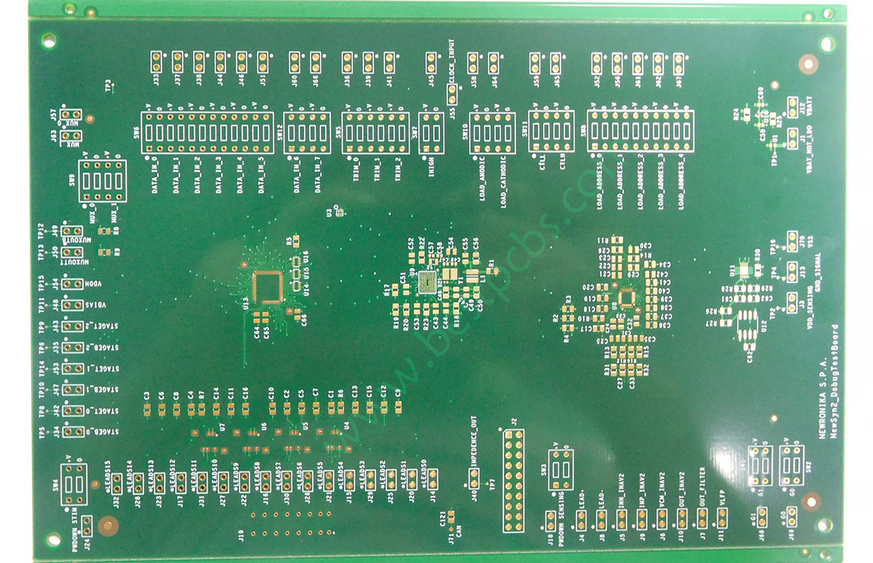
| Green | White |
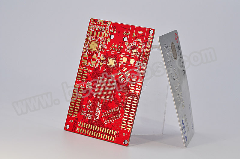
| Red | White |
For the most part,the color of solder mask doesn’t have any effect on PCB’s
functionality.But if the color of the silk screen does not match properly,which may
Cause chromatic aberration(for example,a yellow silkscreen on a black solder mask,
The silkscreen visual may look green)or make reading the silk screen more difficult
To read(for example, a black silkscreen on a light black solder mask).The solder mask will also affect your ability to visually inspect the PCBs. Below are the solder mask comparison from the highest contrast to the lowest for your reference.
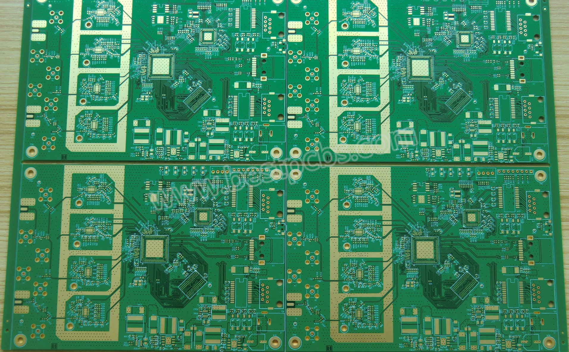
Green
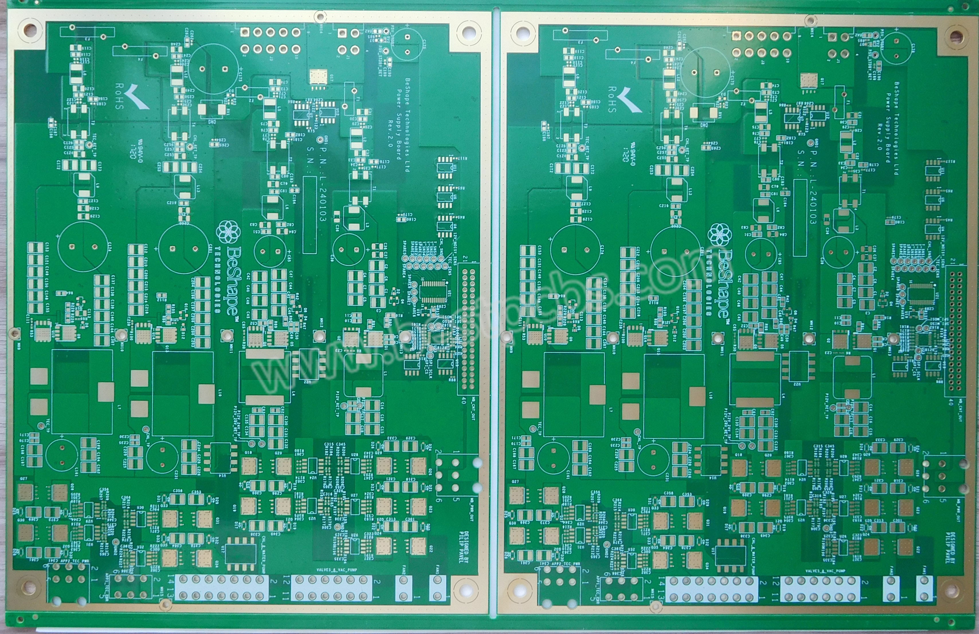
Most customers will choose to use Green solder mask for their project since Green is easy on the eyes and allows for high contrast between traces, planes, and empty space on the PCB. Green solder mask has become an industry standard. High contrast allows technicians to most easily review for manufacturing defects.
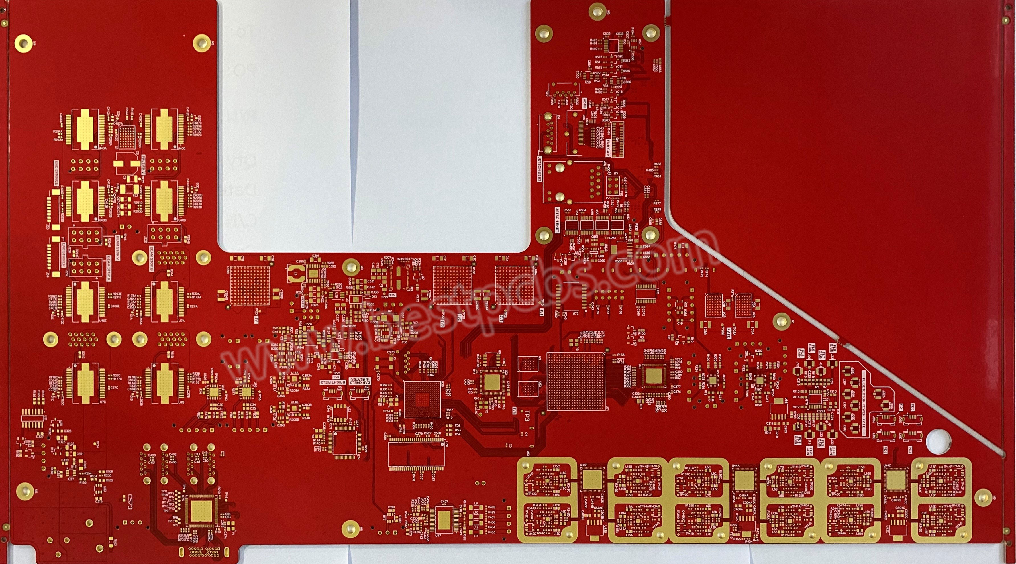
Red
A Red solder mask will provide a bold and clean looking PCB, however the contrast between traces, planes, and empty space significantly lower than it is with a green solder mask. Magnification may be needed when inspecting fine traces on the board for defects with a Red mask. White silkscreen will be better than black silkscreen on a board with red solder mask.
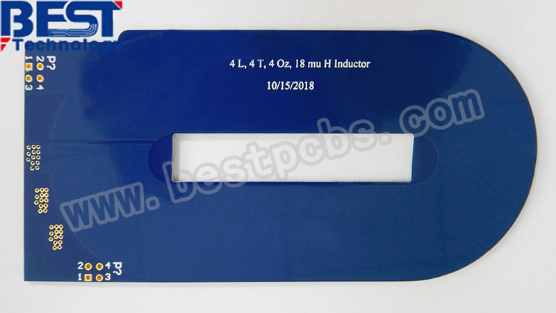
 Blue
Blue solder masks have even lower contrast, and magnification becomes required when inspecting for manufacturing defects. These PCBs look visually pleasing and professional and are a good choice for fully-developed products that will not require trace visibility.
Black
Black masks have almost no contrast between traces, planes and empty space. A Black mask will absorb heat, increasing the danger of overheating for sensitive components. Pay attention that in order to avoid the appearance of color difference as far as possible do not choose the silkscreen like yellow, green, red, or blue. White will be the better choice.

White
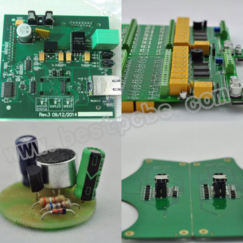
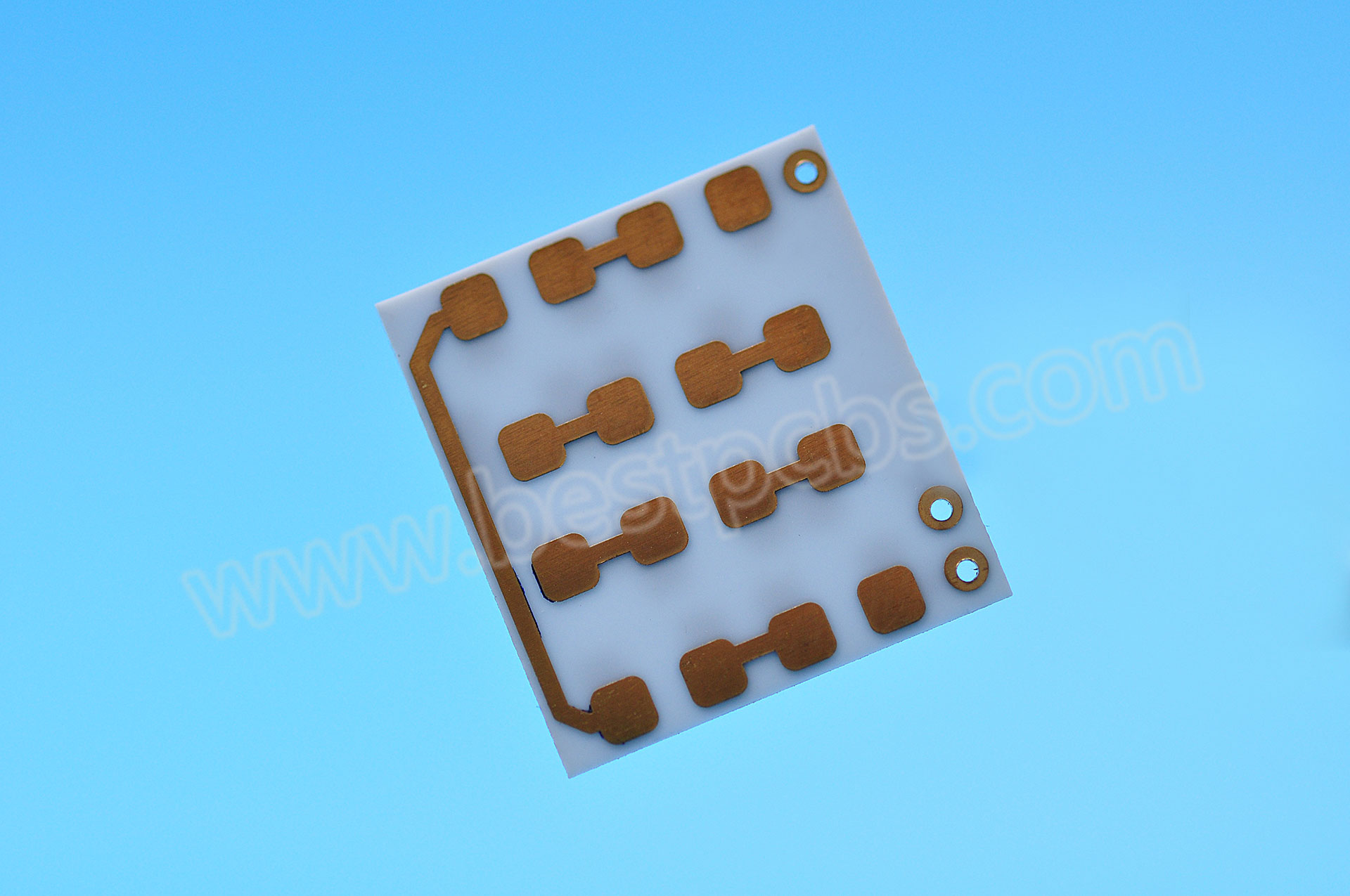
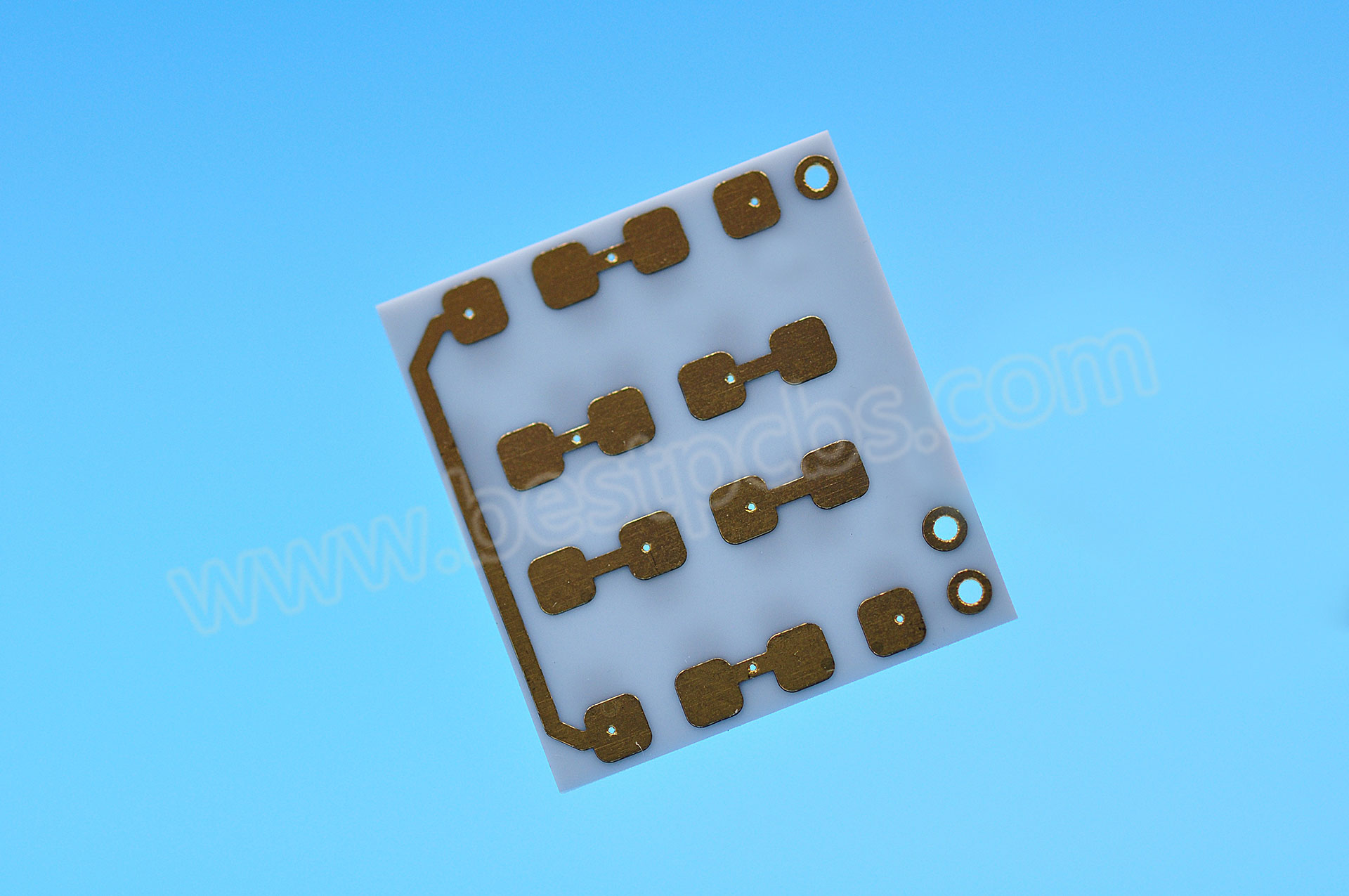
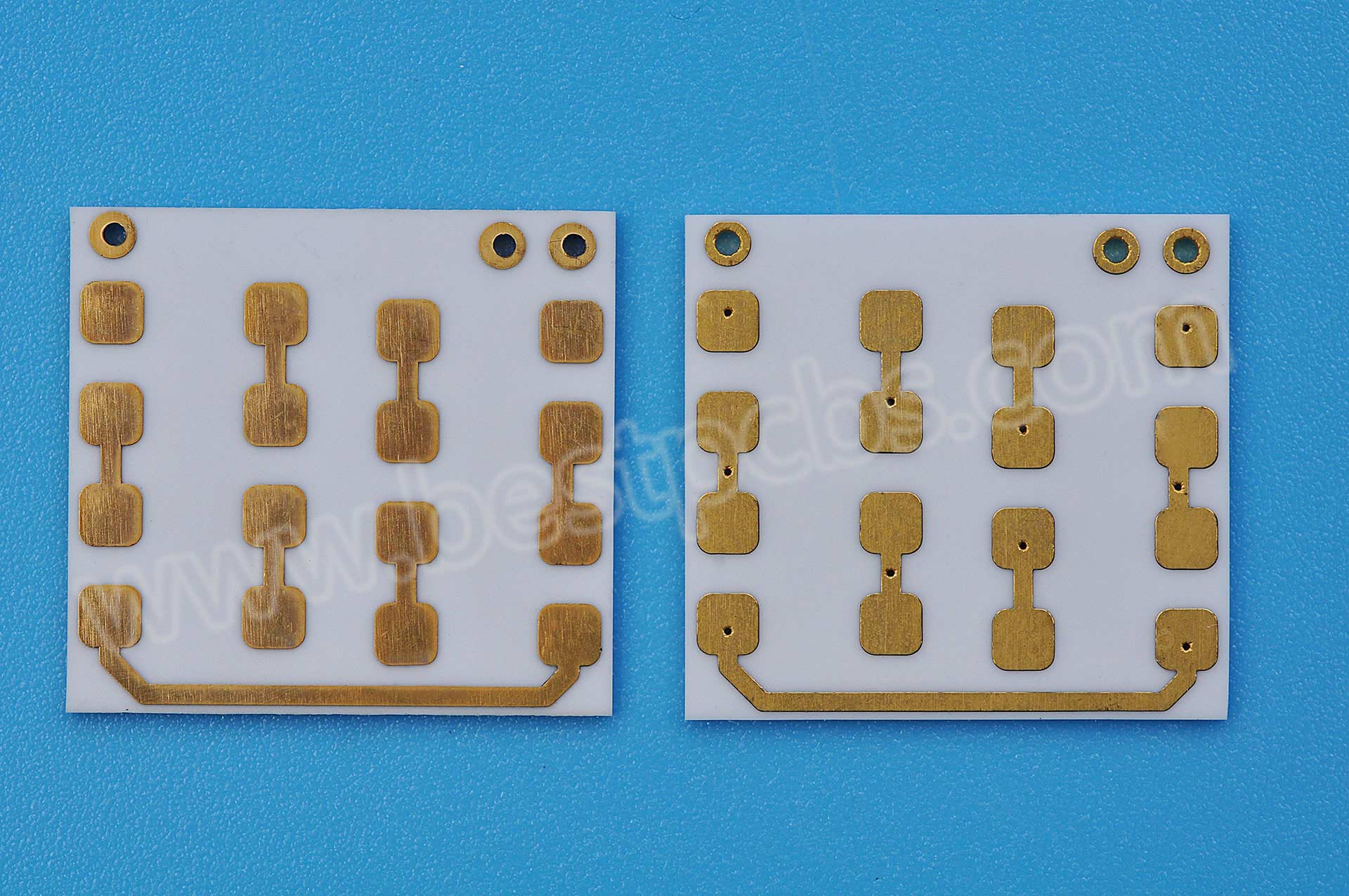
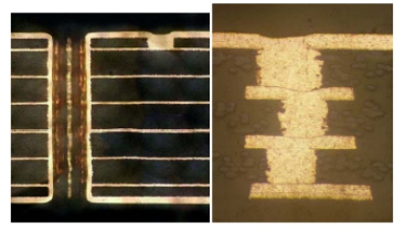
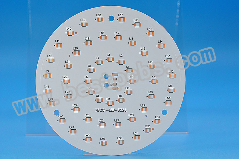
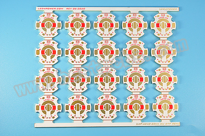
A white mask will be the hardest to clean, and also has the lowest contrast. If possible, we suggest that you avoid choosing white, especially in the prototyping stage. It’s the best choice to use white solder mask for LED board, following pictures for your reference.
If you have other questions about solder mask, welcome to contact us. (Email:sales@bestpcbs.com), we will prove you professional suggestions and solutions.
.JPG)