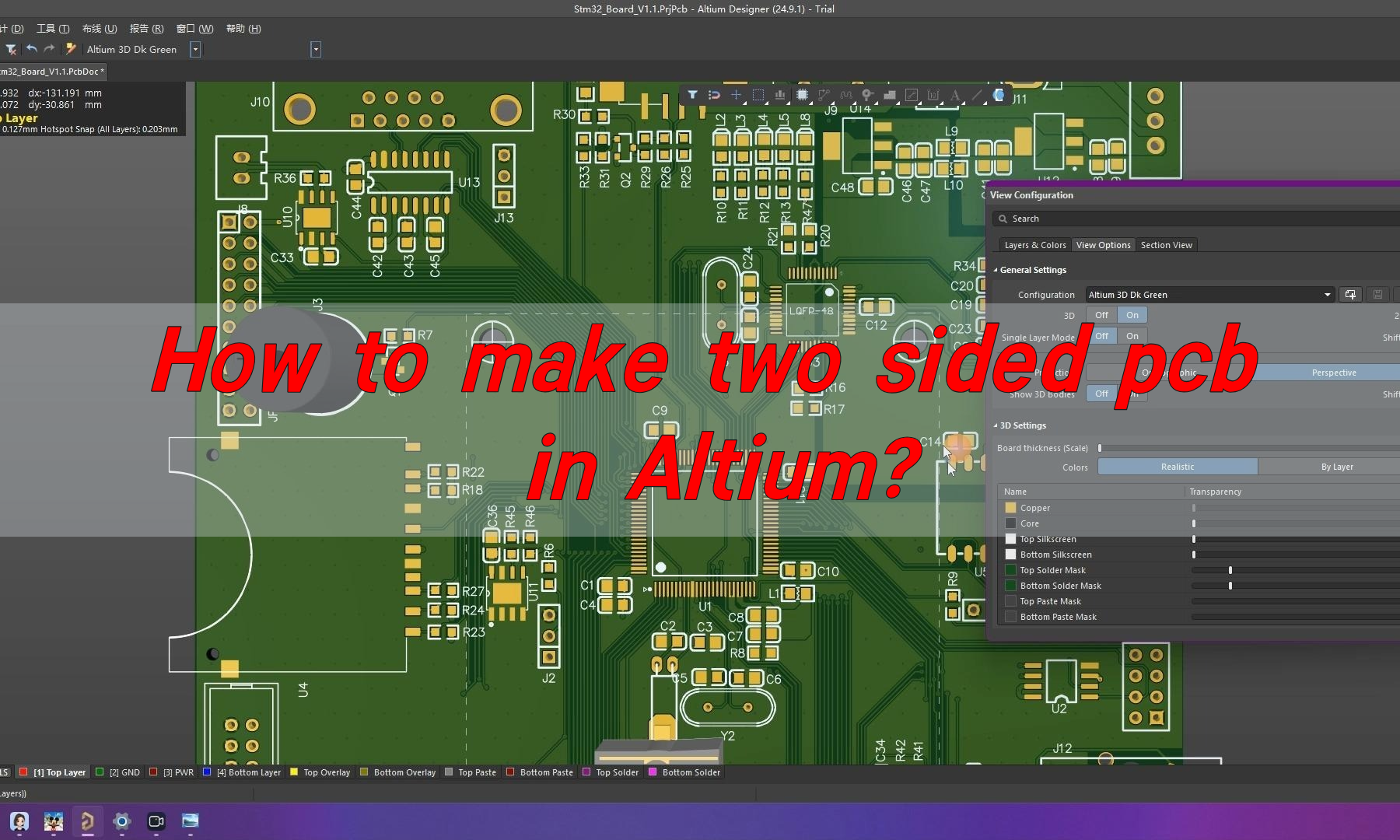
How to make two sided pcb Altium? Be familiar with the interface and basic operations of Altium Designer, accurately design the circuit schematic diagram, reasonably plan the PCB layout, make full use of the double-sided space, conduct fine wiring, ensure signal integrity, and correctly set the rules and parameters to meet production requirements.
What is a double-sided PCB?
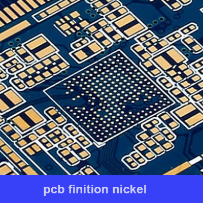
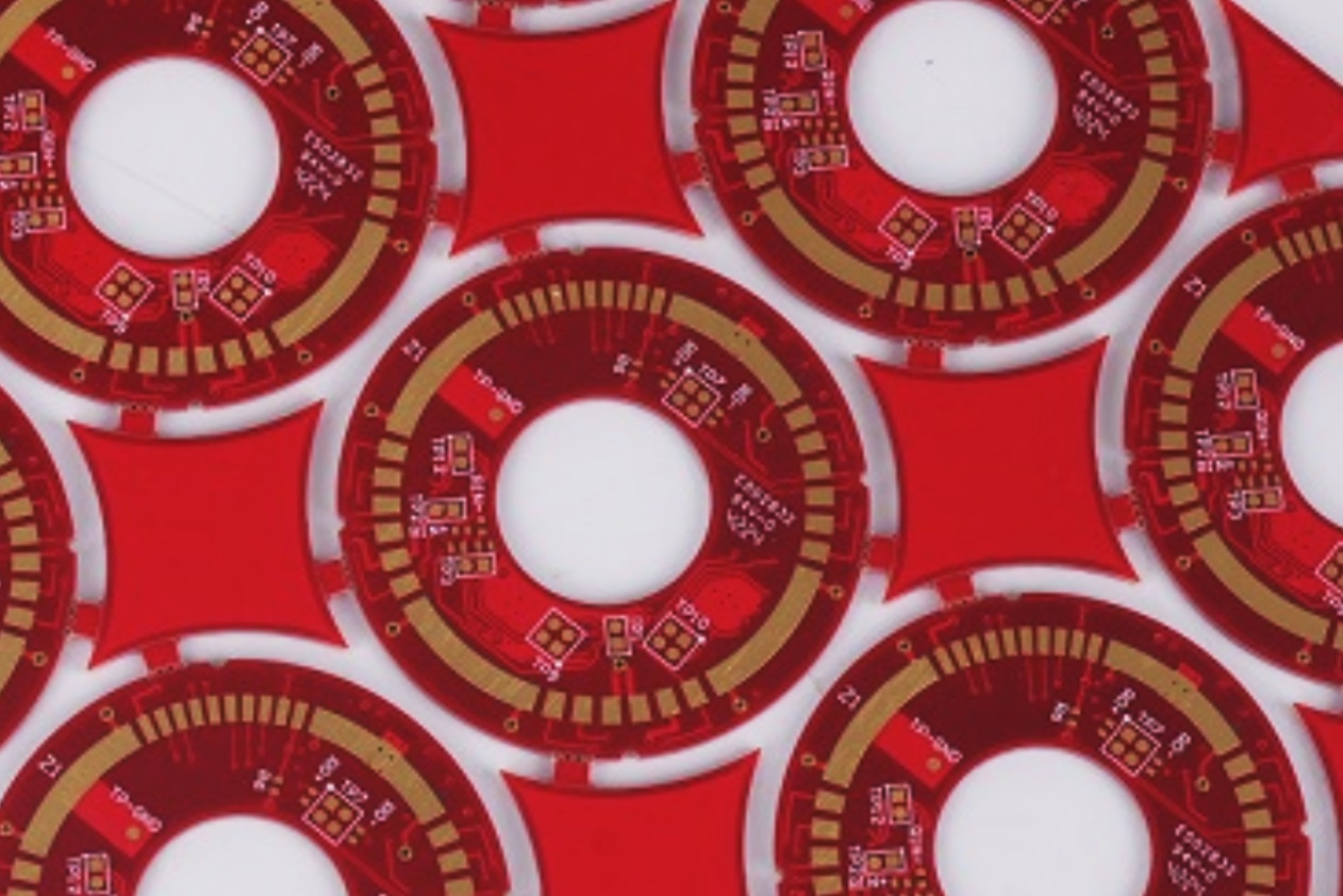
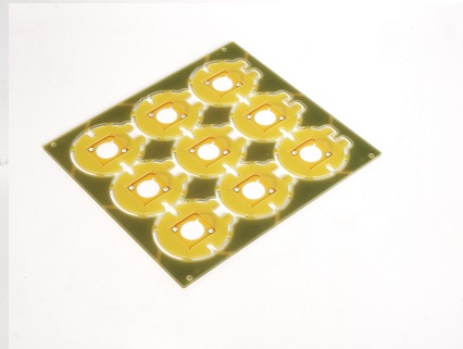
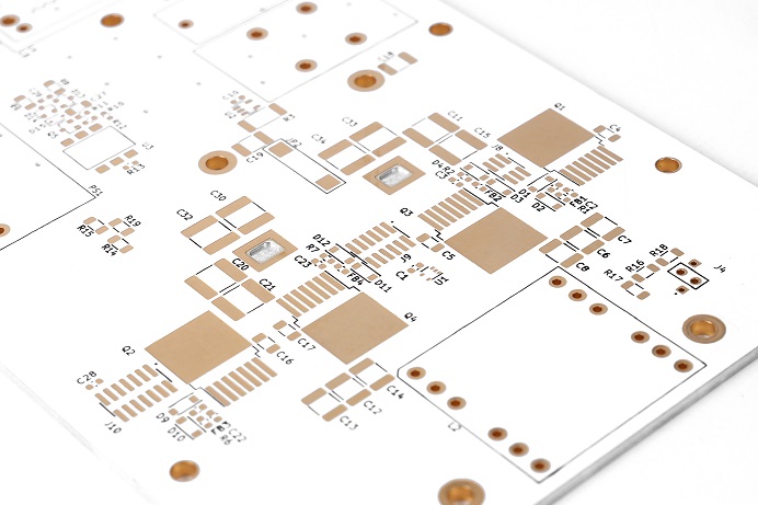
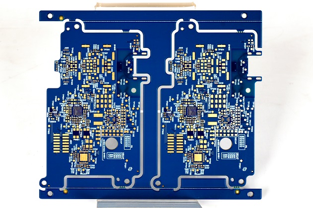
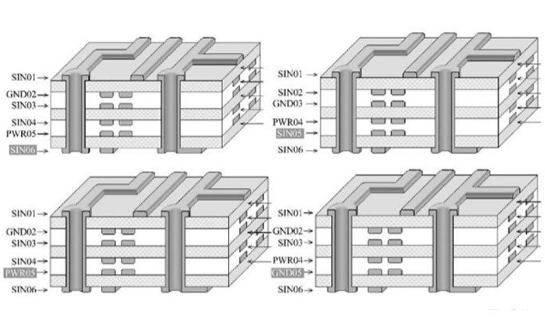
Double-Sided PCB refers to a printed circuit board with conductive copper layers on both sides, and the circuit between the two sides is connected through through holes (small holes). This design enables double-sided PCBs to implement more complex circuit layouts in limited space without significantly increasing the board size.
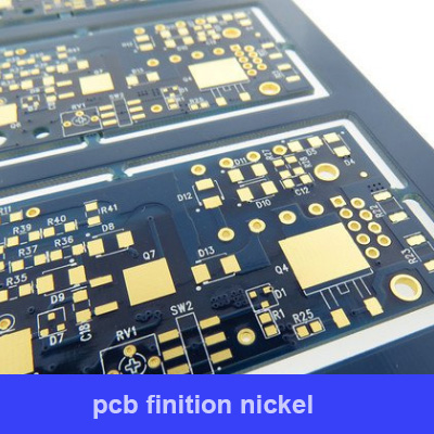
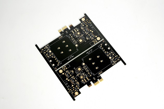
Double-sided PCBs are widely used in various application scenarios that require complex circuit layouts and high-density assembly, such as computers, communication equipment, industrial control, and consumer electronics.
Because it can achieve more complex circuit designs in a limited space, double-sided PCB is particularly suitable for applications that require higher-function electronic equipment, such as smart home equipment, computer hardware, medical equipment, etc.
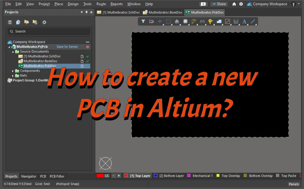
How to make two sided pcb in Altium?
Here are the general steps for making a double-sided PCB in Altium:
- Create a project: In Altium Designer, select “File” > “New” > “Project” to create a new PCB project.
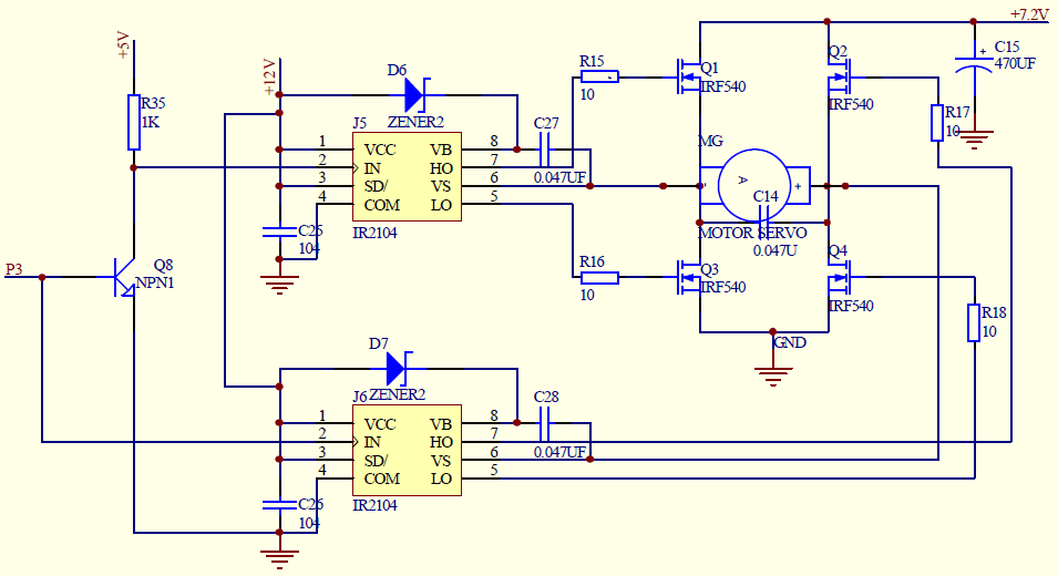
- Draw a schematic: Select “File” > “New” > “Schematic” to create a new schematic file. Add the required components to the schematic and connect them using wires.
- Add package library: If you need to use a custom package library, you need to add it to the project. Select Design > Add/Remove Library and select the desired footprint library.
- Generate PCB: After the schematic is drawn, select “Design” > “Update PCB Document” to import the components and connection information in the schematic into the PCB.
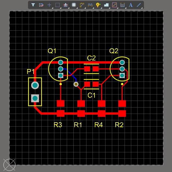
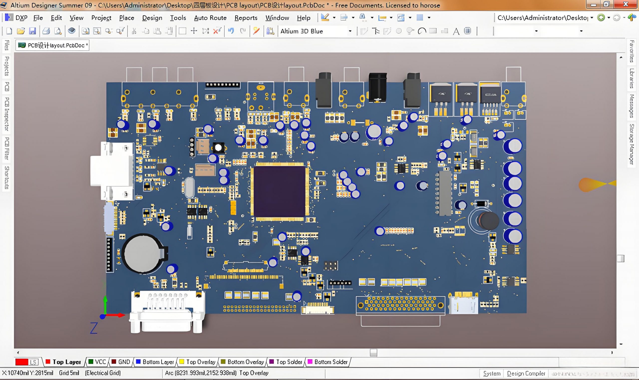
- Layout components: In PCB, components are laid out according to design requirements. You can use Altium’s automatic layout tools or manual layout.
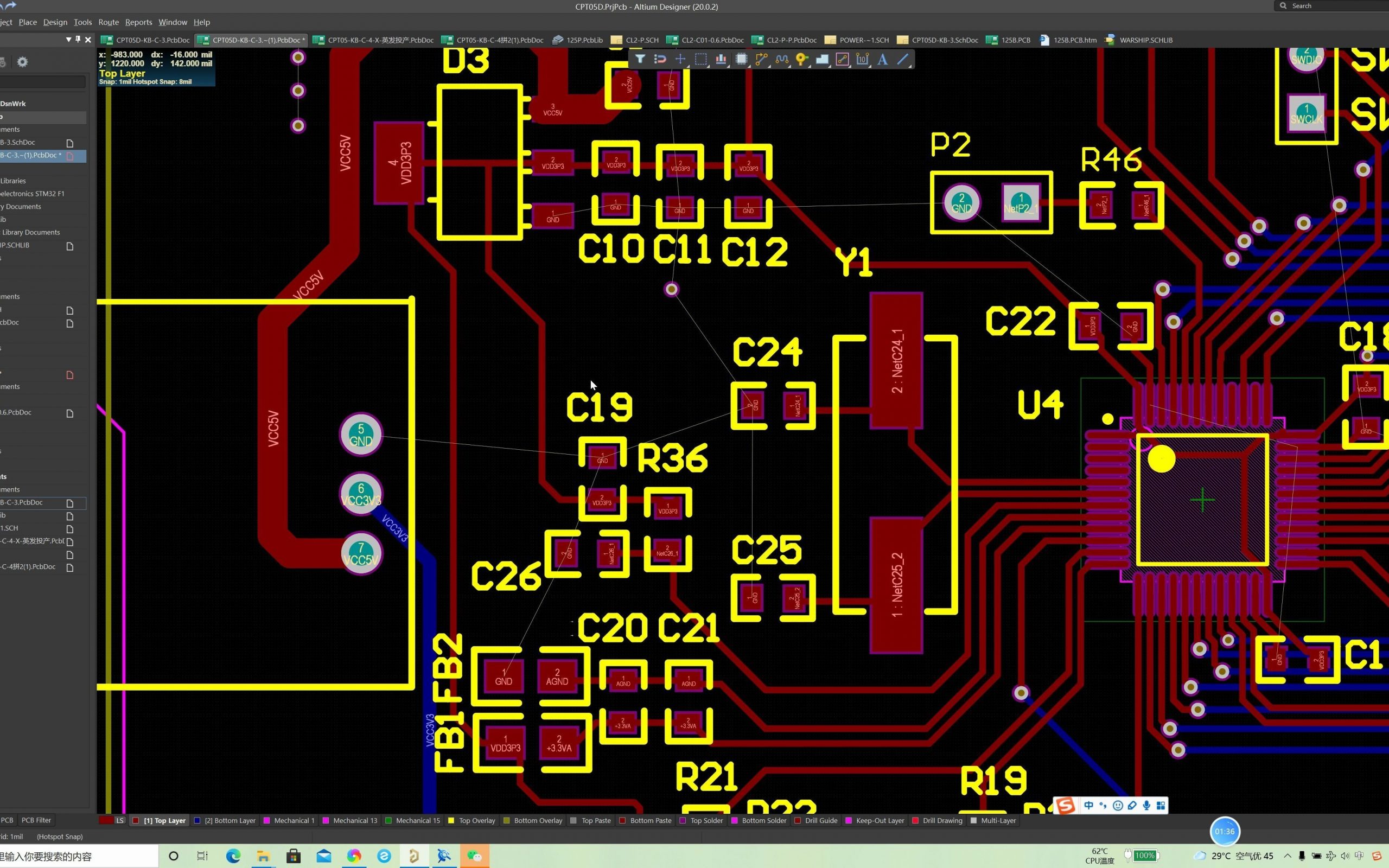
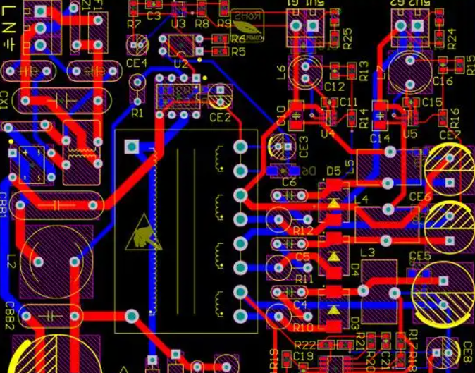
- Routing: Use Altium’s routing tools to route the connections between components. You can choose automatic routing or manual routing.
- Add silkscreens and logos: Add silkscreens and logos to the PCB to easily identify components and connections.
- Check and Validate: Use Altium’s Design Rule Checker tool to check that your PCB design meets requirements. Electrical rule checks, wiring rule checks, etc. can be performed.
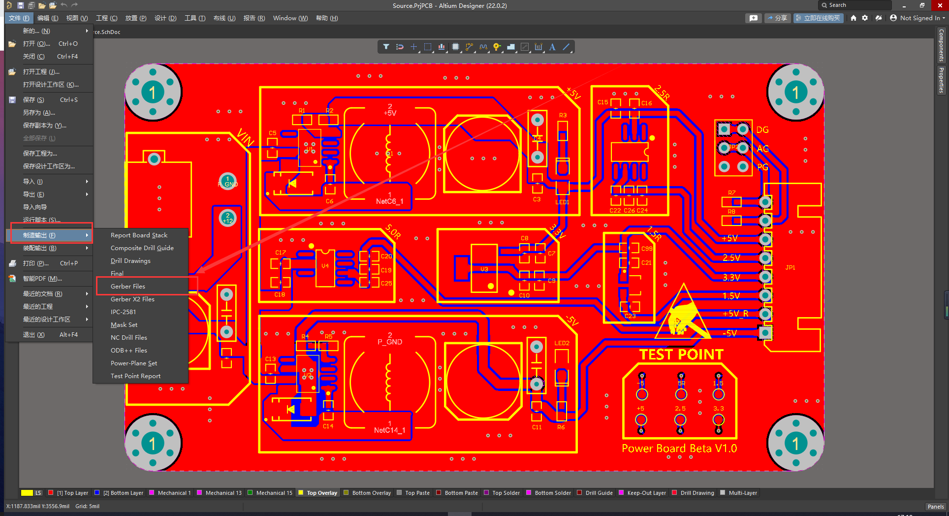
- Generate manufacturing files: After the PCB design is completed, select “File” > “Fabrication Outputs” to generate manufacturing files, such as Gerber files, drilling files, etc.
How to make two-sided PCB?
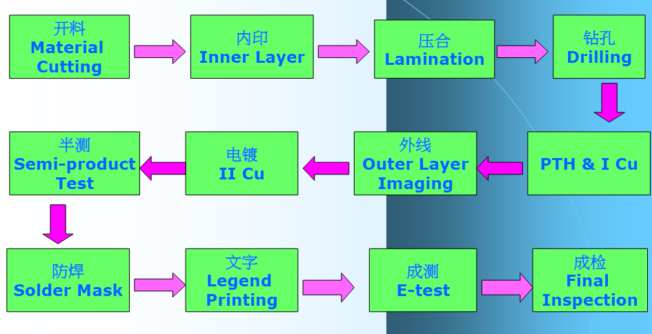
After designing the layout of the double-sided PCB in the PCB design software according to the circuit schematic diagram, the production process begins.
The complete process of making double-sided PCB:
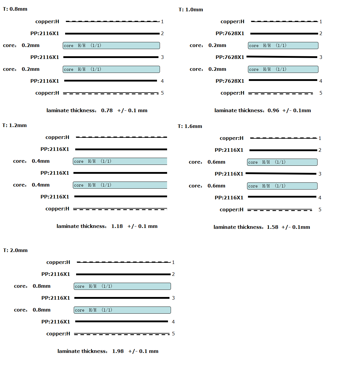
- Preparation materials: Choose a copper-clad laminate covered with copper foil of a specific thickness (such as 18μm, 35μm, etc.) on both sides, and determine the copper foil specifications according to circuit requirements.
- Drilling: According to the drilling documents, use a CNC drilling machine to drill high-precision holes to ensure the connection paths for the circuits on each layer.
- Copper immersion: Place the drilled PCB board in a copper immersion liquid to deposit a thin copper layer on the hole wall, laying the foundation for subsequent copper electroplating and ensuring the reliability of electrical connections.
- Copper electroplating: Use the PCB board as the cathode to energize the copper ion plating solution, thicken the copper layer to the design standard, and enhance the electrical conductivity and mechanical properties.
- Exposure and development: The Gerber file is made into a film. After applying photoresist to the copper-clad board, the film pattern is printed on the board through exposure equipment, and then the unexposed photoresist is dissolved with a developer to initially present the circuit pattern.
- Etching: Use ferric chloride or acidic etching solution to dissolve the copper foil that is not protected by the photoresist, and form precise lines on both sides of the copper-clad board. Then use a film stripping solution to remove the remaining photoresist.
- Make the solder mask layer: Use screen printing to apply solder mask ink of the selected color on the circuits on both sides of the board, and use screen printing to print white character ink on the corresponding positions of the cured solder mask layer to mark component information to facilitate assembly and debugging.
- Drying treatment: Drying fixes the character ink to avoid fading and blurring.
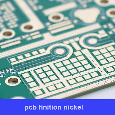
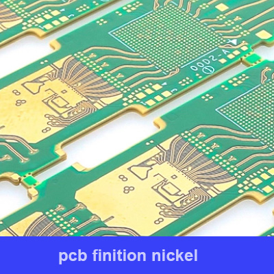
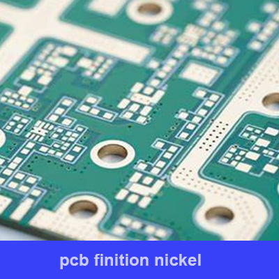
- Surface treatment: Dip tin or spray to coat the pad with tin layer to improve solderability, suitable for products with regular soldering requirements.
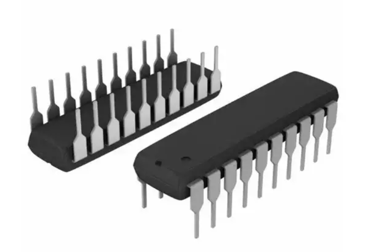
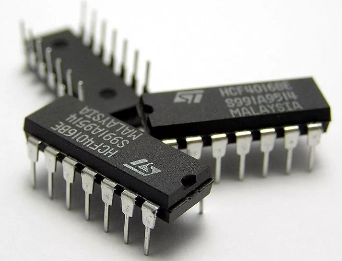
Can you put components on both sides of a PCB?
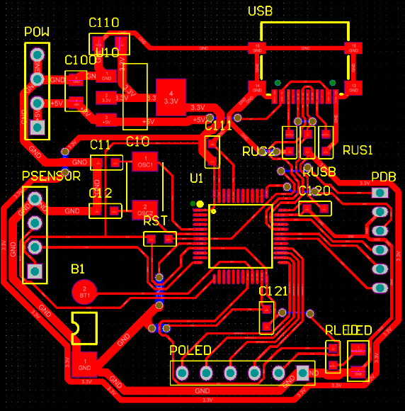
Components can be placed on both sides of the PCB. Both sides of the PCB double-sided panel can be wired and components placed, which can reduce the difficulty of wiring and is suitable for the design of complex circuits.
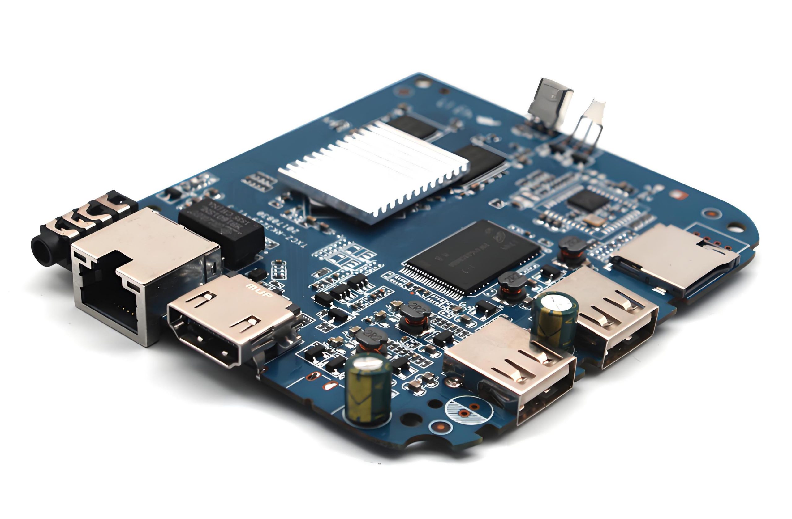
In a double-board design, larger and denser components such as QFP and BGA are usually placed on the top layer of the board, while plug-in components can only be placed on the top layer. Smaller components and components are placed on the other side (bottom layer) of the plug-in components. Chip components with a small number of pins and loose arrangement.
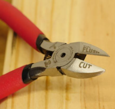
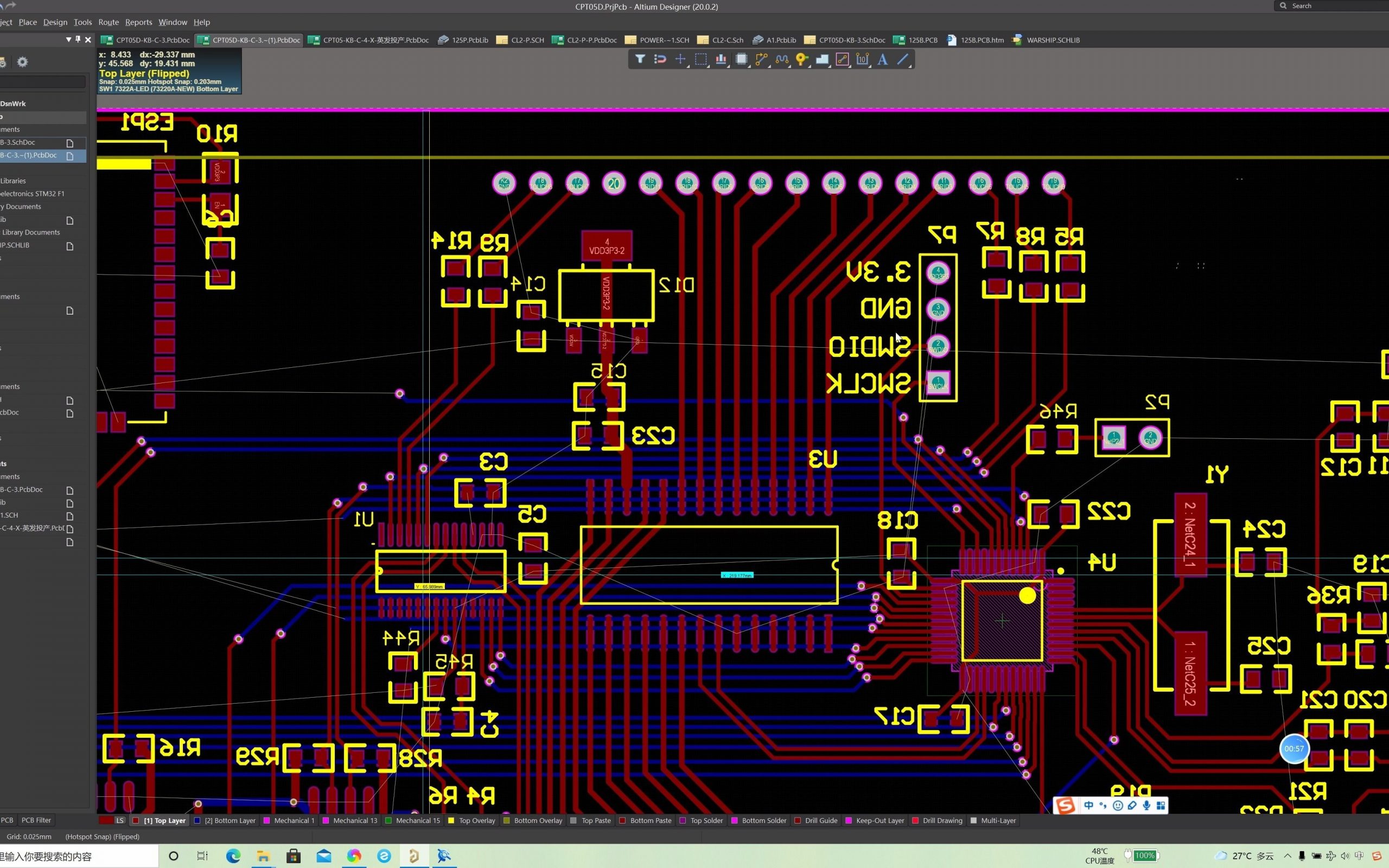
How do you flip a PCB in Altium?
Use the shortcut key: Press the “V” key and then the “B” key to quickly flip the PCB view to the bottom layer. This method is like turning the PCB board over visually, making it easier to view the underlying component layout, wiring, etc.
Operation through the menu: Select the “View” menu, find the “Flip Board” option in the drop-down menu, and click it to flip the PCB view between the top and bottom layers. This method is relatively intuitive and suitable for users who are not familiar with shortcut keys.
How do you flip a component to the bottom in Altium?
Menu operation: Hold down the “Ctrl” key and use the left mouse button to click the components that need to be flipped one by one to select them all. Then follow the menu operation steps for flipping a single component, that is, select “Edit” – “Move” – ”Flip Selection”, so that multiple selected components can be flipped to the bottom together.
Shortcut key operation: First select multiple components, the selection method is the same as above, also hold down the “Ctrl” key and click the components. Then press the “L” key to flip these selected components to the bottom layer at the same time.
How do I mirror graphics in Altium?
In the schematic editing environment, select the component that needs to be mirrored. You can select it by left-clicking the component with the mouse. Then select the “Edit” menu and click on the “Mirror” option. Or use the shortcut key “Ctrl + M” to mirror the component in the horizontal direction. Properties such as the pin connections of the component will not change, only the graphic appearance will be mirrored.
In the PCB editing environment, select the component to be mirrored by clicking it directly with the left mouse button. Select the “Move” submenu under the “Edit” menu and click on the “Mirror Selection” option. The component will be mirrored with the axis perpendicular to the PCB board plane as the axis of symmetry. This is useful when adjusting component layout, especially when you need to flip the component from top to bottom and mirror it at the same time, etc.
In addition, for some regularly shaped components (such as rectangular components), you can also select the component and hold down the “L” key to achieve the effect of flipping and mirroring the component between layers.
How do I rotate a whole PCB in Altium?
Use keyboard shortcuts to rotate in the PCB Editor:
Select the entire PCB (you can select the entire PCB through the “Edit” menu – “Select” – “All”). Press “Space” to rotate the PCB counterclockwise in 90° increments. This is a faster way to rotate, making it easier to adjust the direction of the PCB during the layout and routing process to better fit the workspace or meet specific layout ideas.
Rotate via menu options:
Also select the entire PCB first. Select the “Edit” menu – “Move” – ”Rotate Selection”. In the pop-up dialog box, you can set the rotation angle. The PCB can be rotated accurately according to the design requirements, such as inputting any angle such as 45°, 60°, etc., and then clicking the “OK” button to complete the rotation operation. This method is relatively more flexible and can meet the rotation needs of non-integer multiples of 90°.
During the design process, pay attention to key points, be familiar with the operation of the software, accurately design the circuit schematic, reasonably plan the PCB layout, conduct fine wiring, set correct rules and parameters, and conduct strict inspection and optimization. Only in this way can the quality and reliability of PCB design be ensured and meet the needs of practical applications.