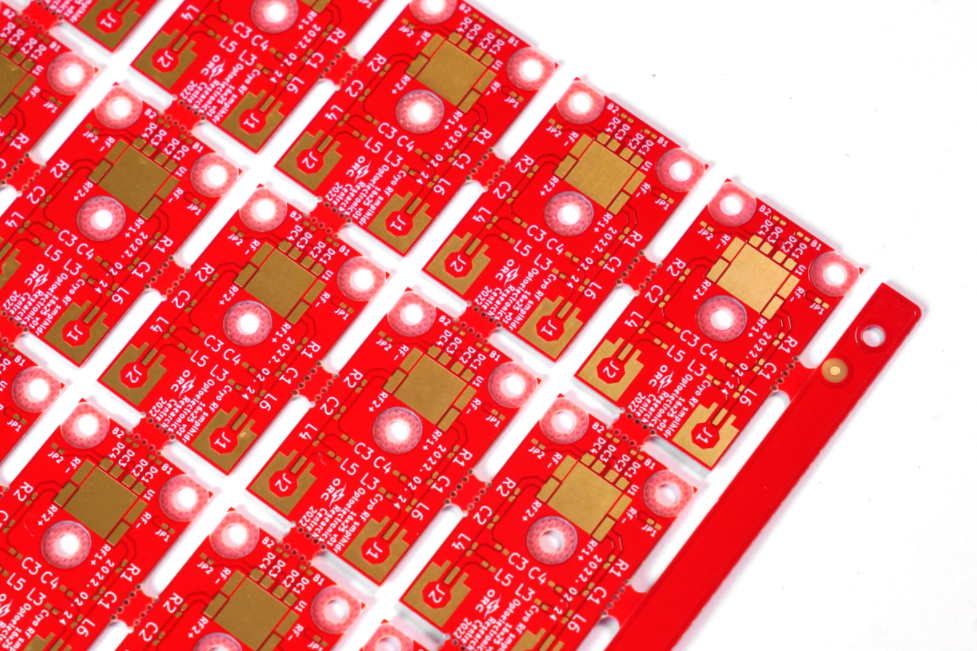
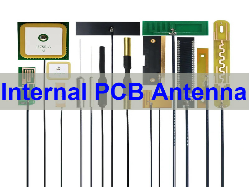
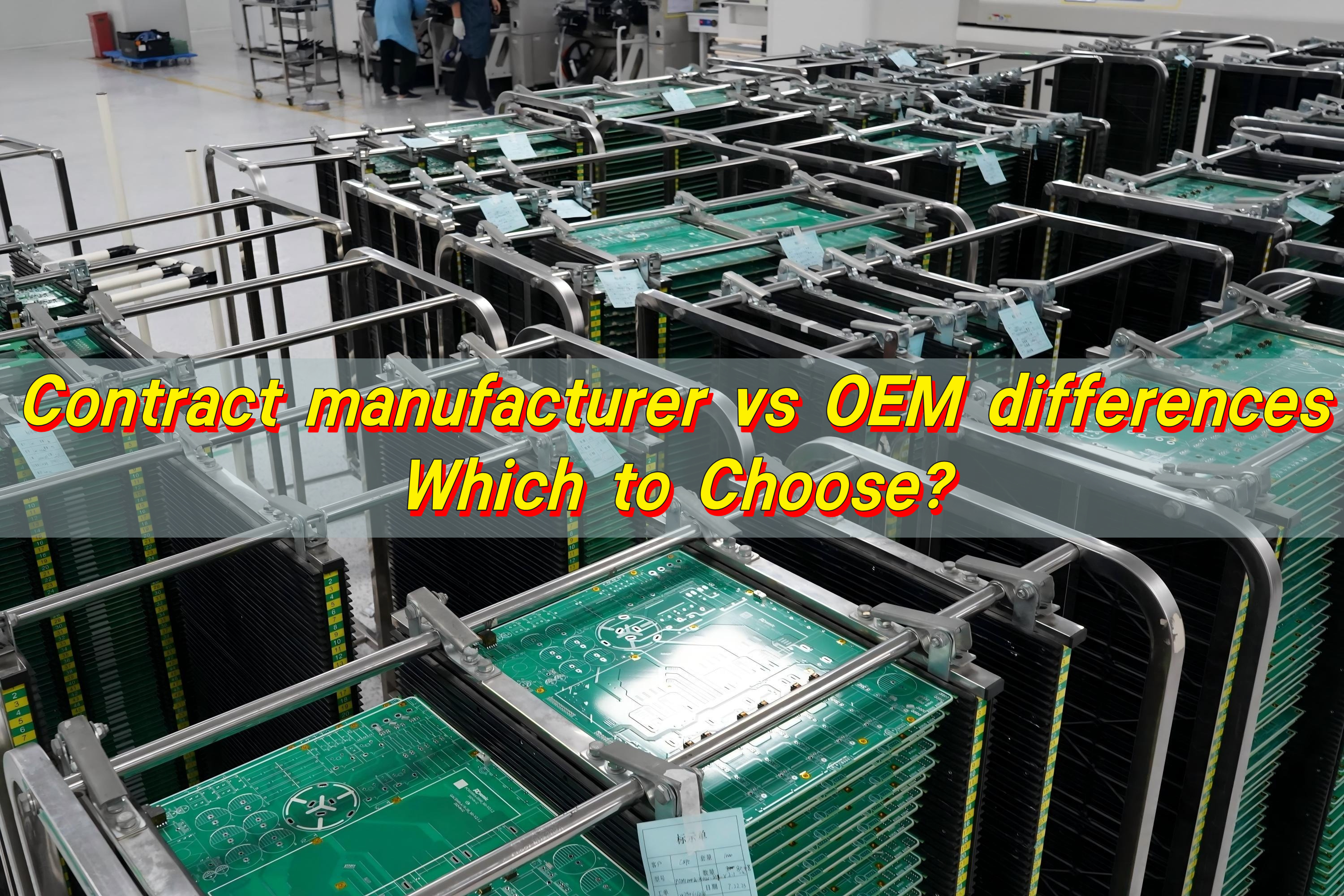
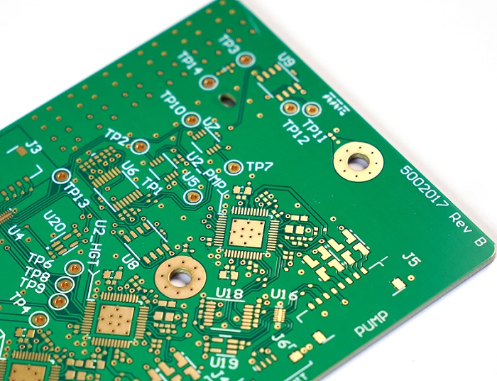
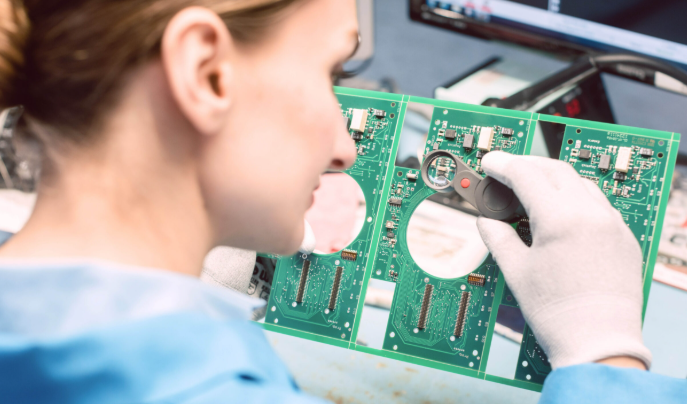
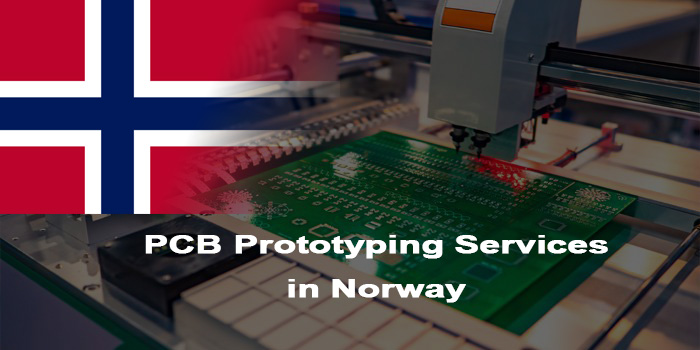
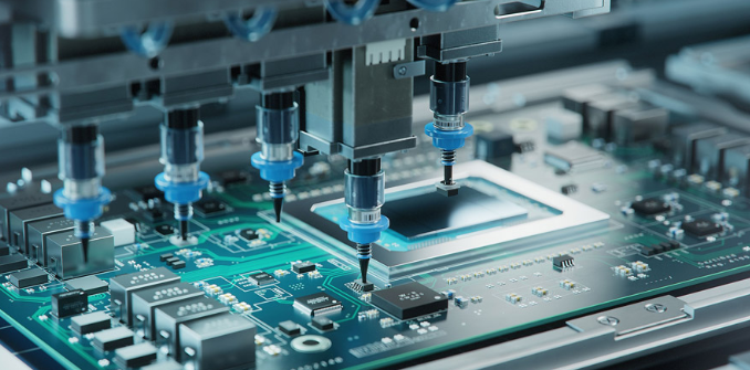
For teams across Norway building industrial equipment, medical devices, aerospace components and advanced electronics, reliable PCB prototyping services in Norway are essential to keep product development on track and avoid costly delays. With over 20 years of global PCB manufacturing experience, EBest Circuit delivers tailored PCB prototyping services in Norway that combine speed, precision and compliance, supporting everything from standard FR4 prototypes to high-frequency, rigid-flex and heavy copper boards for mission-critical applications. We eliminate common prototyping roadblocks, adhere to strict international quality standards, and align every project with unique technical and timeline requirements for consistent, high-quality results.
Common Challenges of PCB Prototyping Services in Norway
- How do long lead times for local PCB prototyping disrupt tight product development schedules in Norway?
- Why is it hard to find manufacturers that support specialized PCBs for medical, aerospace and industrial use in Norway?
- Do limited local prototyping capabilities lead to repeated design revisions and wasted development time?
- How do cross-border communication gaps affect prototype accuracy and compliance with regional standards?
- Why do many prototypes fail due to lack of detailed DFM analysis before production starts?
- How do supply chain delays for specialized components impact PCB prototype turnaround in Norway?
- Is it difficult to access flexible, small-batch prototyping without high minimum order requirements?
End-to-End PCB Solutions from Design to Requirement
Long lead times and limited local prototyping capacity often derail Norwegian projects, and our full-cycle solutions fix this gap directly. We cover every step from design validation to final shipping, cutting out middlemen and redundant delays for consistent progress.
Solve Long Lead Time & Limited Capacity Issues: We run dedicated prototype production lines to avoid delays from bulk orders, with 24-hour expedited options for urgent Norwegian projects. Our large-scale manufacturing space supports fast turnaround, even for complex, custom board designs.
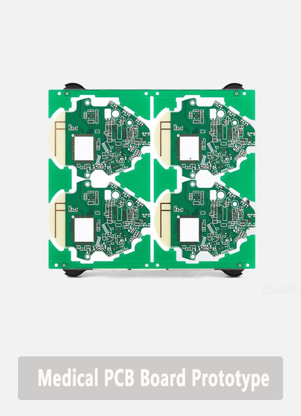
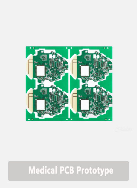
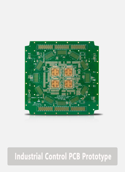
Fix Specialized PCB & Compliance Gaps: We manufacture medical, aerospace and industrial-grade PCB prototypes with full regulatory certifications (ISO 13485, AS9100D, IATF 16949). This meets strict regional standards and supports high-performance boards local providers cannot handle.
Eliminate Component Sourcing & Communication Delays: Our global component supply chain cuts wait times for specialized parts, with in-house stock for critical materials. We provide clear, consistent project updates to avoid cross-border communication gaps and ensure accuracy.
Avoid Costly Design Mistakes with Free DFM Analysis: We include free DFM analysis for every Norwegian project, catching design flaws early to eliminate repeated revisions and wasted development time. This ensures your prototype is manufacturable on the first try.
Why Choose EBest for PCB Prototyping Services in Norway?
With 20+ years of global PCB manufacturing expertise, EBest delivers data-backed PCB prototyping services in Norway that directly solve your top project pain points. We focus on speed, compliance and reliability, with proven results for medical, aerospace and industrial electronics projects across Norway.
- Unmatched Fast Lead Times: We offer 24-hour expedited prototype shipping and 3-5 business day standard turnaround, cutting project timelines by up to 70% compared to local Norwegian providers’ 7-14+ day lead times, keeping your development on track.
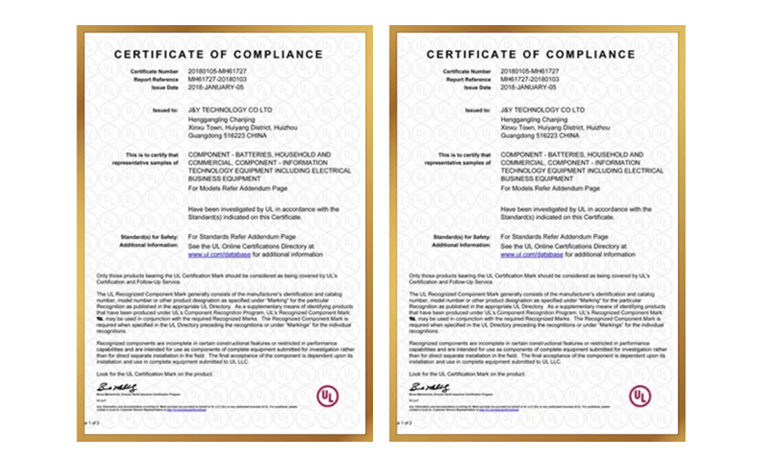
- Full Industry Regulatory Compliance: We hold 7+ global certifications including IATF 16949, ISO 13485:2016 and AS9100D, with 100% of our Norwegian prototypes passing regional and European compliance audits on the first submission for high-stakes projects.
- Free Comprehensive DFM Analysis: Our complimentary DFM analysis catches 98% of pre-production design flaws, eliminating costly reworks; this premium service is included free for all Norwegian orders, while most local providers charge extra for it.
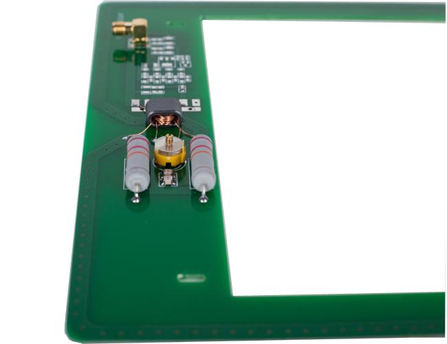
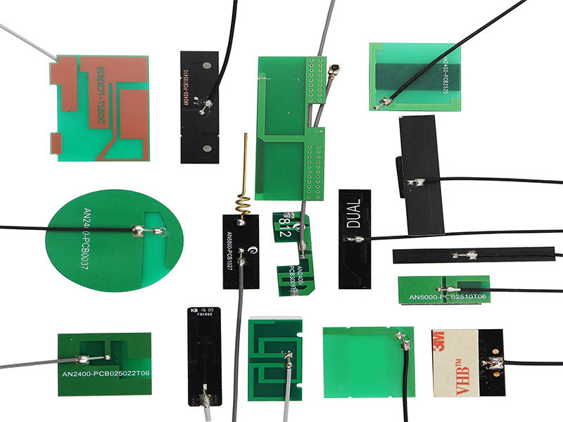
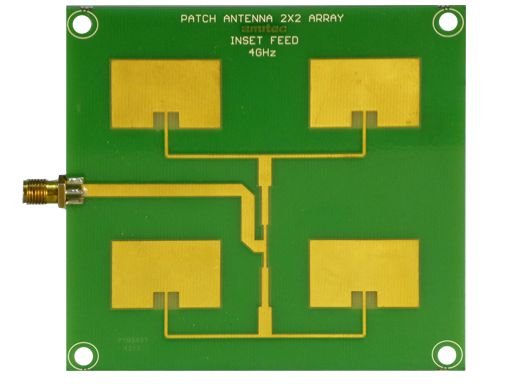
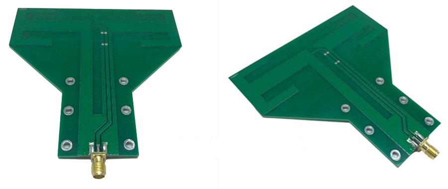
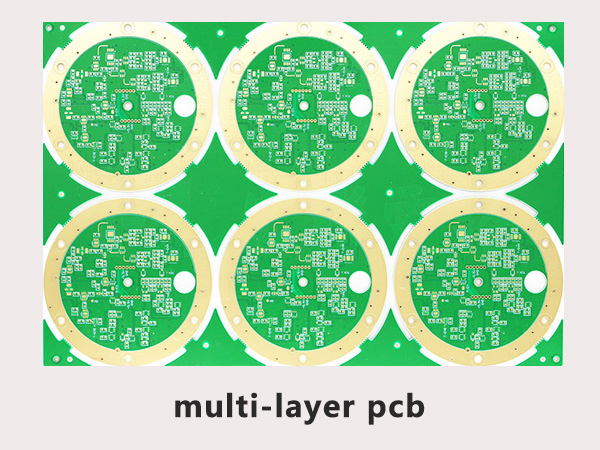
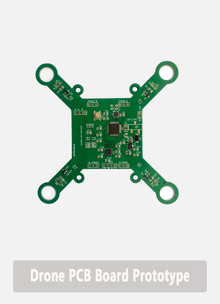
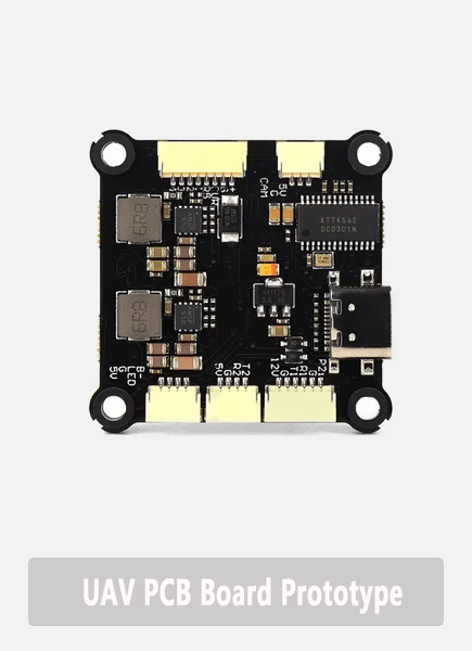
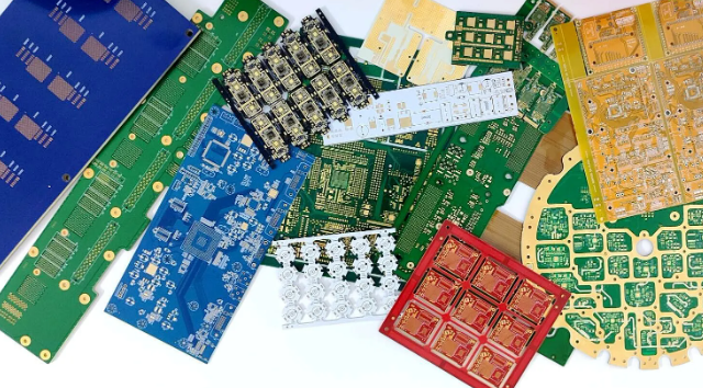
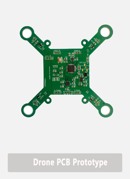
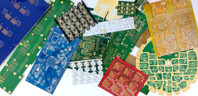
- Full-Spectrum Specialized PCB Prototypes: We manufacture 12+ high-performance PCB types (up to 20 layers) including HDI, rigid-flex and heavy copper boards, covering complex needs that 60% of local Norwegian manufacturers cannot support with basic FR4 boards only.
- Flexible Small-Batch Prototyping: We support prototype orders from 1 piece to 500 pieces with no minimum order requirements, ideal for R&D testing; 85% of our Norwegian clients rely on our low-volume prototyping for early-stage development.
- Stable Global Component Supply Chain: Our global sourcing network and in-house stock of 3,000+ critical components cut component lead times by 80%, eliminating supply chain delays that disrupt local prototype timelines for Norwegian projects.
- Dedicated Prototype Production Lines: We run 4 exclusive prototype-only production lines, separate from mass production, eliminating 90% of delays from bulk order backlogs and prioritizing your prototype timeline at all times.
- Full Project Transparency & Visibility: We provide real-time order tracking and daily status updates for all Norwegian projects, resolving cross-border communication gaps; 99% of clients report full clarity on their prototype timeline from start to delivery.
Quick Lead Time for Your PCB Prototype Service
| Layers | Normal Service | Fastest Service |
| 1 | 7 Days | 24 H |
| 2 | 8 Days | 24 H |
| 4 | 10 Days | 48 H |
| 6 | 10 Days | 72 H |
| 8 | 12 Days | 72 H |
| ≥10 | TBD | TBD |
Free DFM Analysis: Avoid Costly PCB Prototyping Mistakes in Norway
Our free DFM (Design for Manufacturing) analysis is a core, value-driven part of PCB prototyping services in Norway, built to cut unnecessary reworks, avoid schedule delays and prevent costly prototype failures long before production starts. Industry data shows nearly 70% of PCB prototype setbacks in Norway stem from undetected design flaws caught too late, which derail timelines and waste development resources for medical, aerospace and industrial projects.
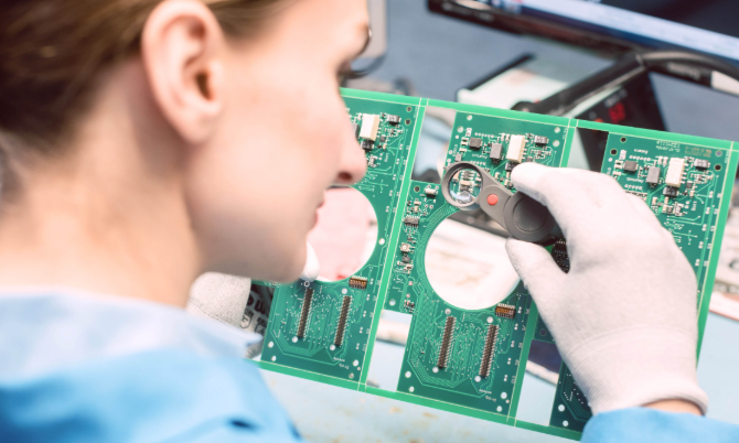
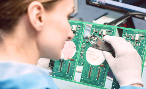
Our senior PCB engineers conduct a full, detailed review of every design file, checking line width, impedance control, layer alignment, component placement and material compatibility to catch critical risks. We deliver a clear, actionable report with targeted fixes, ensuring your prototype is fully manufacturable, meets strict industry compliance standards, and passes testing on the first run. This free service has helped dozens of Norwegian high-stakes projects avoid costly delays and repeated production runs.
Rapid PCB Prototyping in Norway: How EBest Ensures Your Project Stays on Schedule
EBest keeps your rapid PCB prototyping project on schedule through optimized workflows, dedicated prototype production lines, proactive communication and global supply chain stability. Unlike many manufacturers that prioritize large mass production orders, we focus on fast, efficient prototype turnaround to support Norway’s agile product development teams.
Our Schedule-Guarantee Prototyping Process
- Dedicated Prototype Production Lines: Separate lines for prototype orders to avoid delays from bulk production jobs.
- Real-Time Order Tracking: Full visibility into your prototype status from design approval to shipping
- Stocked Critical Components: In-house inventory of high-demand components to eliminate sourcing delays.
- Expedited Quality Testing: Streamlined compliance and functional testing for prototypes, no unnecessary delays.
- Priority Shipping to Norway: Pre-negotiated fast shipping routes for reliable, on-time delivery.
For a Norwegian industrial automation client, we delivered 12 custom heavy copper PCB prototypes in 48 hours, keeping their equipment testing timeline on track and avoiding project downtime. For a medical device client, we expedited a rigid-flex prototype order while maintaining ISO 13485 compliance, meeting their strict regulatory and timeline demands.
Our PCB Prototyping Process: Transparent, Fast, and Built for Your Requirements
Our PCB prototyping process is fully transparent, customer-centric and customized to your exact technical requirements, with no hidden steps or generic production. Every step is tailored to match your board type, industry compliance needs and timeline, ensuring full alignment with your project goals.
- Design Submission & Free DFM Review: Submit your design files, our engineers complete free DFM analysis and share feedback within 24 hours
- Quote & Approval: Fixed, detailed quote with clear timeline; start production once approved
- Custom Prototype Fabrication: Precision manufacturing using your specified materials (FR4, ceramic, metal core, etc.)
- Quality Inspection & Testing: Full compliance and functional testing to meet ISO, UL and industry-specific standards
- Packaging & Shipping: Secure packaging and fast shipping to your Norway location
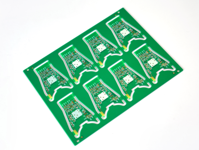
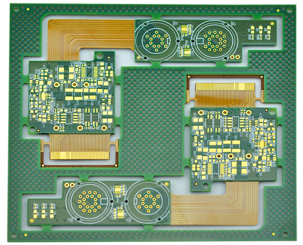
We handle every prototype type, from basic single-sided boards to complex HDI, high-speed and impedance-controlled PCBs, with consistent quality and transparency at every stage.
Get a Quote for Your PCB Prototype in Norway
Securing a free, accurate quote for PCB prototyping services in Norway takes just a few simple steps with EBest. Our streamlined process cuts wait times, avoids back-and-forth delays, and delivers a detailed, no-obligation quote tailored to your Norwegian project.
Step 1: Submit Your Complete PCB Design Files & Project Details: Send your finalized PCB design files (Gerber, Drill, or BOM files) alongside core project specs: prototype quantity, board material (FR4, ceramic, metal core, etc.), layer count, and any special requirements (impedance control, heavy copper, medical/aerospace compliance).
Step 2: Free Preliminary DFM Check & Scope Review: Our senior PCB engineers run a quick, complimentary DFM scan to spot basic manufacturability risks and confirm your design aligns with prototype production standards. We verify all specs match your timeline and compliance needs for Norway.
Step 3: Receive Your Custom, No-Obligation Quote Within 24 Hours: We deliver a fully detailed quote with clear turnaround times, production scope, and full transparency, no hidden fees. The quote includes our standard 3-5 day turnaround or 24-hour expedited option for urgent Norwegian projects.
Step 4: Approve Quote & Start Production Planning: Once you approve the quote, we lock in your production timeline and begin full DFM analysis (included free). We immediately reserve space on our dedicated prototype lines to ensure on-time delivery to Norway.
Step 5: Prototype Production & Timely Delivery to Norway: We execute production per your approved specs, complete strict quality testing, and ship directly to your Norwegian location with tracked logistics. You get real-time updates until your prototypes arrive safely.
FAQs About PCB prototyping services in Norway
Q1: What types of specialized PCBs can be prototyped for medical and aerospace use in Norway?
A1: We prototype a full range of high-regulation PCBs for Norway’s medical and aerospace sectors, including ISO 13485-compliant medical device PCBs, AS9100D-certified aerospace PCBs, rigid-flex boards, high-frequency RF PCBs and heavy copper industrial PCBs. All prototypes adhere to strict European and international compliance standards, with full traceability and quality documentation.
Q2: How quickly can urgent PCB prototypes be delivered to Norway?
A2: We offer 24-hour expedited prototyping for urgent orders, with prototypes shipped the same business day after approval and production. Standard prototype orders to Norway arrive in 3-5 business days, with tracked international shipping and guaranteed on-time delivery for time-sensitive projects.
Q3: Is free DFM analysis included for all Norwegian PCB prototype orders?
A3: Yes, free comprehensive DFM analysis is included for every prototype order for Norway-based projects. Our engineering team reviews all design files to identify manufacturability issues, compliance gaps and performance risks, providing actionable fixes before production to eliminate reworks and delays.
Q4: Can you handle small-batch PCB prototyping for Norway-based product development teams?
A4: Absolutely. We specialize in flexible small-batch and low-volume PCB prototyping with no high minimum order requirements, perfect for Norway’s product development, R&D and startup teams. We support prototype runs from single pieces to mid-volume batches, with the same quality standards as large production orders.
Q5: What quality certifications ensure PCB prototypes meet Norwegian and European standards?
A5: EBest holds IATF 16949, ISO 9001:2015, ISO 13485:2016, AS9100D, REACH, RoHS and UL certifications, all aligned with Norwegian and European industry regulations. Every prototype undergoes strict quality testing to meet these standards, making them suitable for medical, aerospace, industrial and automotive applications across Norway.