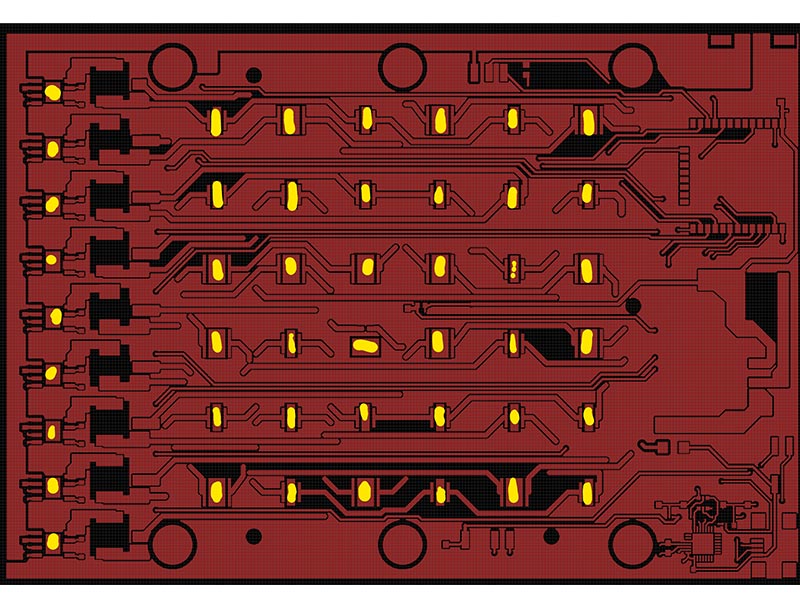
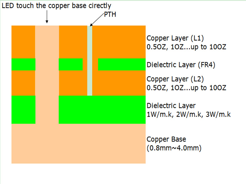
SinkPad PCB is a type of Copper base PCB used in thermoelectric separation application. It generally used for high power LED, the pad of LED touch the copper base directly, so that the heat generated by LED will dissipate quickly, which can achieve the best heat dissipation and conduction.
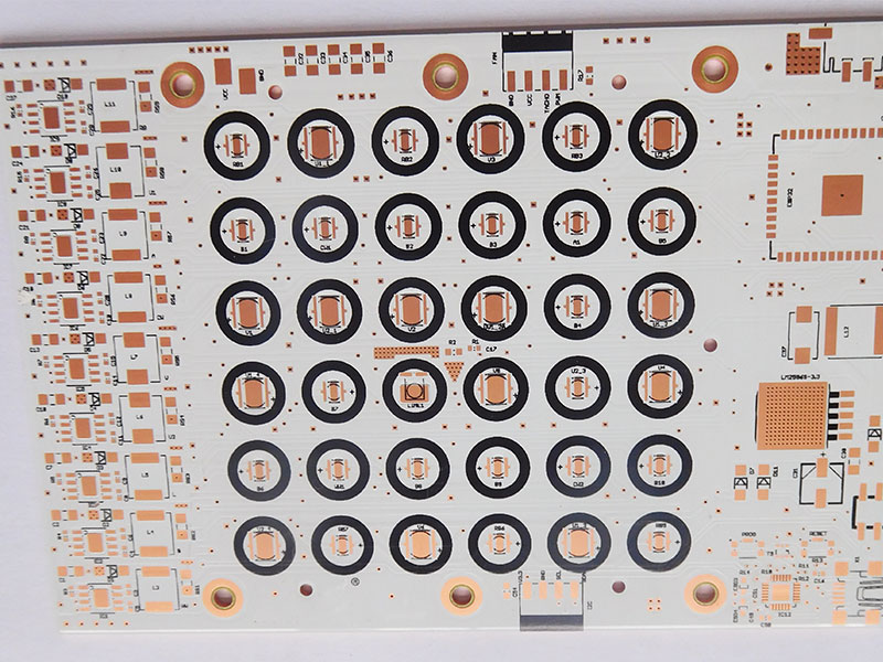
sinkpad gerber
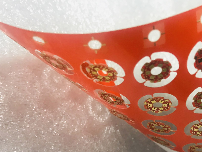
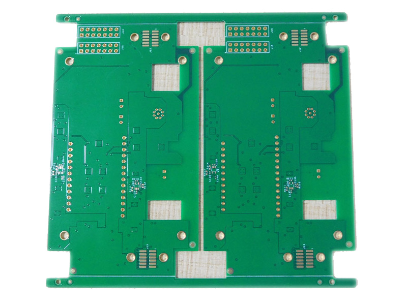
sinkpad pcb
In another words, it is a technology that require to increase the path of the LED pad to the copper base to accelerate the heat emission from the base material. The copper base is vital while it also cost higher.
Then in order to lower cost, can SinkPad PCB use aluminum base instead copper base for heat dissipation?
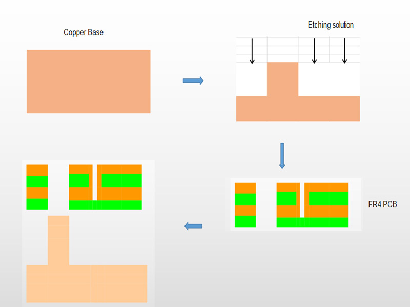
The answer is NO. As you can see the below manufacturing steps, the SinkPad will etch the copper base into convex platform with Copper Etching Solution, then hollow out the Double Layer FR4 PCB, and do lamination with the convex platform.
sinkpad pcb manufacturing steps
However, regarding of current technical conditions, since aluminum or aluminum alloy cannot directly react with acid, the reaction process is too complex and difficult to control, which will increase the difficulty of etching the LED pad platform. Considering the scrap rate, the process of etching LED pad platform with aluminum is more complex and the overall cost is higher.
It is widely known that BeO with high thermal conductivity (200-250W/m.k). High dielectric constant 6-7 (0.1MHz) and dielectric loss tangent is 10-4 (0.1GHz), extremely high working temprature. It is ideal material for ceramic PCB, lots of engineers want to use it as DBC ceramic PCB substrate.
But it is not popular in ceramic PCB market, comparing with Al2O3, AIN, Si3N4, or ZrO2, as the powder of BeO is extremely poisonous.
The poison gas is produced by the reaction between oxygen, Cu and BeO under 1065-1085 degrees Celsius, so it is limited to make cooper on BeO substrate, it has caused ALN (Aluminium Nitride) is becoming more and more popular.
Right now, only few countries are using BeO to make ceramic PCB, such as USA, Russia and China. USA had biggest capability to make BeO , and here in China, there’re still some companies to make BeO raw material and among them, a few companies to produce direct copper bonded (DCB) on BeO because of environment limitation.
Though BeO is not popular for DBC technology, but it is feasible for thick film technology, because when the mentalization of Ceramic PCB, the conductor (Au or AgPd) on BeO substrate was made by silk-screen printing, and drying temperature is only around 850C, no need to under high temperature environment, so there is no chemical reactions, no environment issue.
Below the thick film ceramic PCB manufacturing process for your reference.
EBest Circuit (Best Technology) is a full turn-key assembly service company, we can supply the assembled board with very nice and clean surface.
Do you want to know how we control the cleaning process of PCBA? We would like to share the full cleaning process.
As we know, flux is used when soldering electrical components to a printed circuit board.
After assembly process finished, we need to remove all the unnecessary flux paste or other solder flux/ residue in order to avoid any quality issue.
Although it is a simple work, but to prepare some tools and preparation is necessary and important. Like wash board water, dust-free cloth, brush,Tweezers, static bracelets, finger gloves
Here is the how the cleaning process we made:
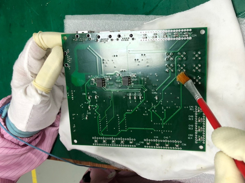
Step1:
Use brush to brush the solder joint and solder flux on the soldered PCB. Applying some alcohol or acetone onto the brush, do not use too much pressure, as this may cause the solder point to break. Repeat the procedure as necessary, to remove remaining flux residue on the PCBA.
Step1: Brush the solder joint and solder flux on the soldered PCB
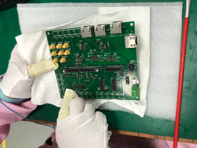
Step2:
Wipe with a clean dust-free cloth to clean the assembled PCB.
Keep board clean and tidy to make sure no impurities and finger marks. Do the same process for bottom side.
Step2:Wipe with a clean dust-free cloth to clean the assembled PCB.
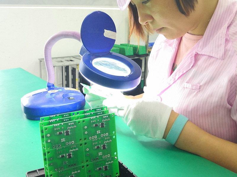
Step3:
When above step finished, keep the board for an extra day to let the board dry enough before packing. Best QC guys will do final inspection for the finger prints under light. this will be helpful to check the cleaning result further.
Step3: final inspection for the finger prints under light
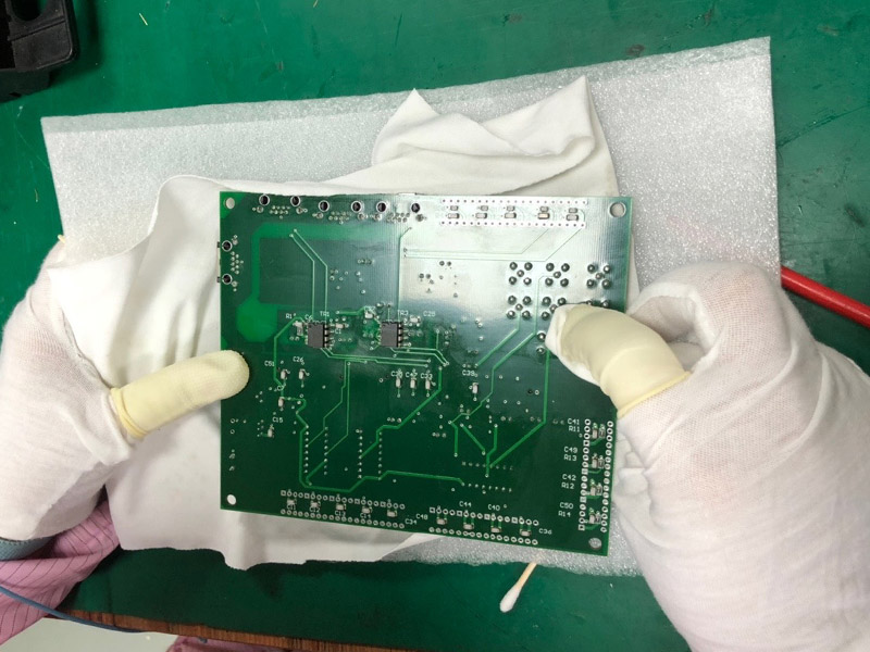
Step4:
Finally, use dust-free cloth to do the final cleaning and let the board dry and clean enough before package.
Step4: use dust-free cloth to do the final cleaning.
Above are the process for how we clean the assembled boards.
Best Tech is a very professional manufacturer in printed circuit board and assembly. We clean each of assembled boards as the procedure we showed above.
If you are interesting to know more process for how we control the quality for the PCB assembled boards, contact us at any time, we will show you more.
As we know, the extra thin PCB means the thickness of printed circuit board is more thin than normal PCB, which is refer to a thickness smaller than 0.4mm for 1L/ 2L & 4L PCB. For extra thin PCB, we know they are all very thin and are easily to be broken, so the option for the surface treatment of the extra thin PCB is very crucial.
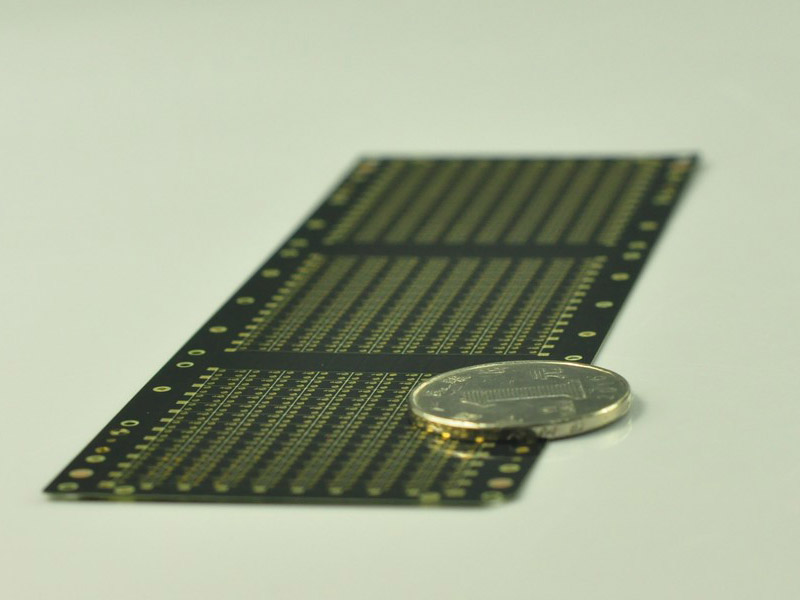
0.15mm extra thin FR4 PCB_EBest Circuit (Best Technology)
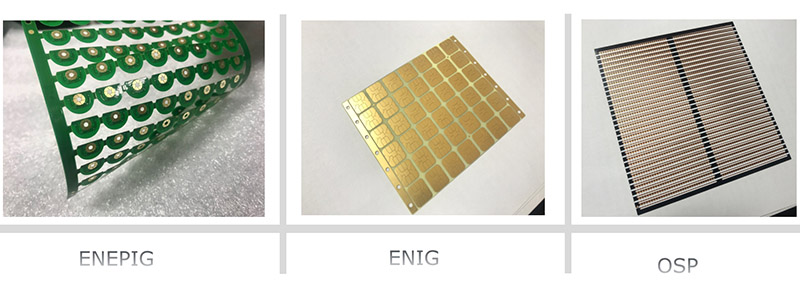
Generally, there are 3 kinds finishing can be recommended for the extra thin PCB. It is OSP, ENIG (Electroless Nickel Immersion Gold), and ENEPIG.
extra thin pcb finishing
But you may want to ask that lead-free Tin is also a common finishing for the PCB. Why not recommend LF HASL?
That’s because while LF HASL Process, the PCB will be easy to be blew away, people will use heated compressed air to leveling (blowing) on the coating molten tin (lead) solder, during this process, the traces will be easy to be broken as well.
So normally, we will not recommend the LF HASL finishing for an ultra thin FR4 PCB.
HASL lead-free is only suitable for a board with minimum thickness of 0.6mm, while the standard gold immersion surface coating can support PCB with a minimum thickness of 0.2mm. For the surface treatment of ENEPIG , which plate only needs to be about 0.1 microns for palladium and about 0.1 microns for gold, (palladium is a precious metal that is much harder than gold), so for board with ENEPIG finishing, its surface will looks more smooth, that’s also why it is the most recommended surface treatment for an extra thin PCB.
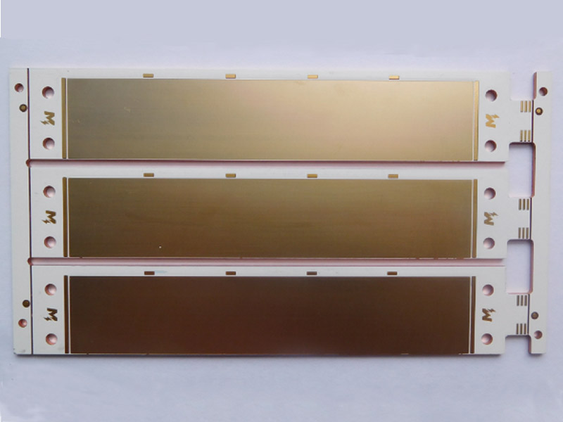
0.13mm extra thin Rigid FR4 PCB_EBest Circuit (Best Technology)
If you are searching for an extra thin PCB, feel freely to ask or send your inquiry to us. We will be pleased to share you more information regarding the extra thin PCB.
SinkPad PCB, also called Heat Sink or DTP (direct thermal path) PCB, it is a type of Copper base PCB used in thermoelectric separation application. It generally used for high power LED, the pad of LED touch the copper base directly, so that the heat generated by LED will dissipate quickly, which can achieve the best heat dissipation and conduction.
SinkPad PCB
Thermoelectric separation technology is based on the higher heat dissipation requirements of high power electronic products, which needs to meet two basic conditions:
1.LED pad touches the base substrate directly.
It means we need to increase the path of the LED pad to the base substrate to accelerate the heat emission from the base material.
Two layers SinkPad PCB Stack up
2.Higher heat dissipation substrate materials
Copper has a thermal conductivity of 401W/m·K, while aluminum has a thermal conductivity of 237W/m·K. Obviously, copper has better thermal conductivity because of its high density, high mass. Therefore, a SinkPad PCB usually means a SinkPad copper base PCB.
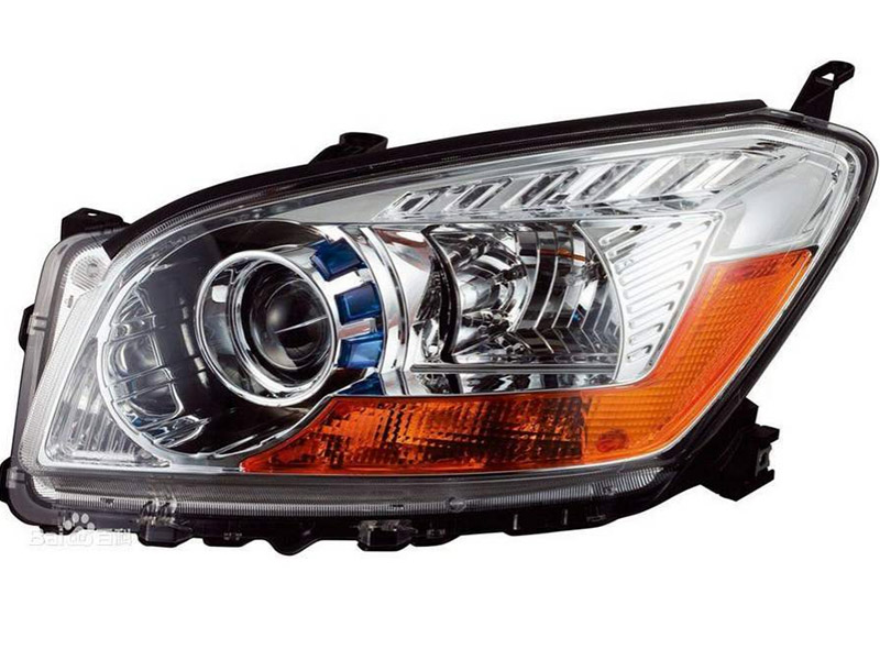
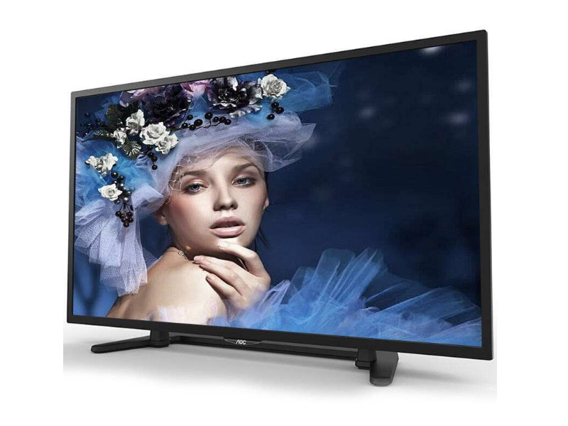
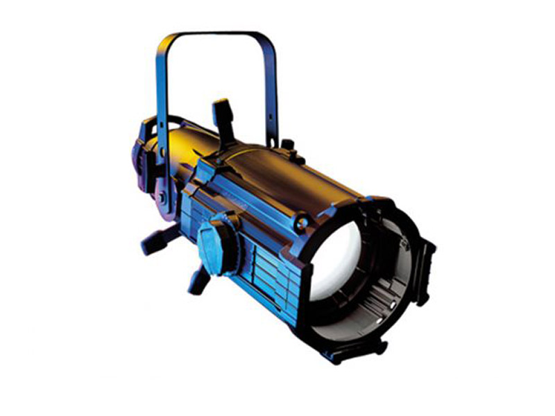
If we observe carefully, we will find that most of the high-quality surface light lamps in the market use COB light source, such as LED spotlights, Automotive, LED Backlight for LED TV, etc. What are the advantages of such choice?
Automotive
LED Backlight for LED TV
LED spotlights
First of all, we need to how the COB differ from the common MCPCB. “Chip-On-Board” Metal Core PCB is a type of MCPCB used in thermoelectric separation application. By using COB, the micro-chip (also known as “die”) directly touch the metal core where the heat dissipate, and electrically interconnect the trace of circuit board (wire-bonding) so that power supply can be provided.
High thermal conductivity(137W/m.K), High insulation, High pressure resistance
High reflectivity: mirror aluminum≥98% (The reflectivity of Taiyo Soldermask used in common MCPCB is 75-80%, the highest is only 90%)
BAS15191
BAS15192
Since the COB is packaged directly on the MCPCB, it’s easy assembly for high powers LED, direct heat dissipation through the substrate can not only reduce the manufacturing process and cost of the bracket, but also have the advantage of reducing heat dissipation resistance. So the spotlight produced by COB technology will be lighter, more flexible and able to realize more possibilities on the stage.
If you are also interested in COB, please feel free to contact me, I’m looking forward to communicating more with you.
In recent years, there are more and more customers request to manufacture PCB with high Tg, in the following we would like to describe what is high Tg PCB.
fr4 170tg
Normally high Tg refers to high heat resistance in PCB raw material, the standard Tg for copper clad laminate is between 130 – 140℃, High Tg is generally greater than 170℃, and middle Tg is generally greater than 150℃. Basically the printed circuit board with Tg≥170℃, we call high Tg PCB. As the rapid development of electric industry, especially for the computer as the representative of electronic products, developing toward the high performance, high multilayer requires PCB substrate material with higher heat resistance to ensure high reliability. On the other hand, as a result of development of SMT, CMT with high density pcb assembly technology, the PCB manufacturing with small hole size, fine lines and thin thickness are more and more inseparable from the support of high heat resistance.
fr4 170tg
If the Tg of PCB substrate is increased, the heat resistance, moisture resistance, chemical resistance and stability of printed circuit boards will be improved as well. The high Tg applicates more in the lead free pcb manufacturing process.
Therefore, the difference between general FR4 and high Tg FR4 is, in the hot state, especially in the heat absorption with moisture, the high Tg PCB substrate will perform better than general FR4 in the aspects of mechanical strength, dimensional stability, adhesiveness, water absorption and thermal decomposition.
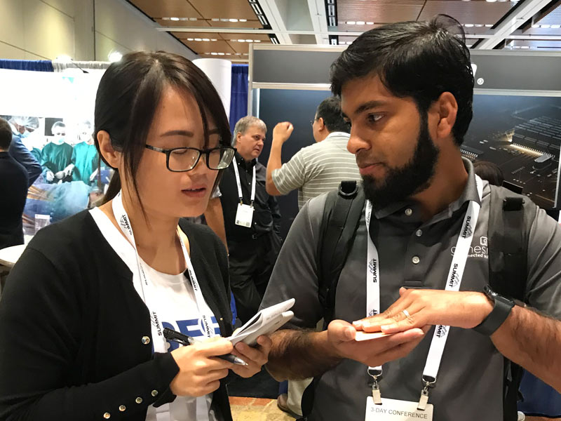
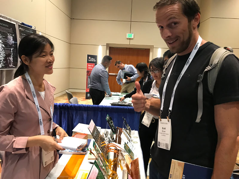
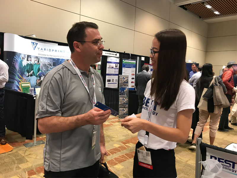
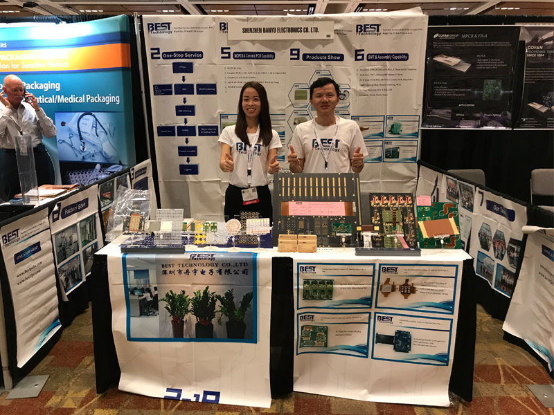
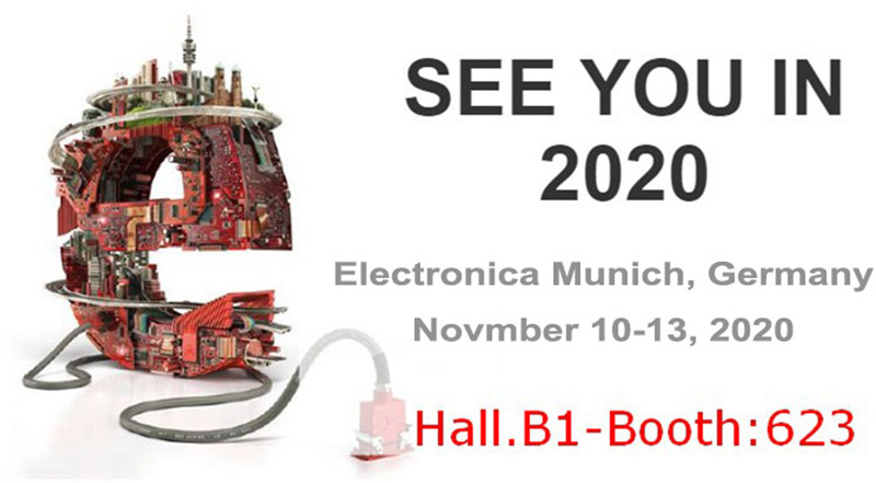
EBest Circuit (Best Technology), a China- based assembly manufacturer will be exhibiting at electronica Munich2020 in Bavaria, Germany at booth No. 623(Hall B1) from November 10, 2020 to November 13, 2020(Western Time). Actually, we have participated in this exhibition for continuous 2 years. Here are some pictures for your reference.
pcb exhibition
pcb exhibition
pcb exhibition
pcb exhibition
At our exhibition booth, attendees will be able to learn more about our company for PCB manufacturing and PCB assembly technology.
For interested professionals, EBest Circuit (Best Technology) had on hand experts to offer detailed insights and experience on PCB assembly, covering PCB prototype and low/high-volume production. For more information on PCB assembly and fabrication, welcome to visit our booth.
You are warmly welcome to see how we can manage the components wastage and efficiency to help save your time, money and energy.
About electronica Munich:
Electronica is the international trade show for electronic components, systems and applications and shows the full range in all its diversity in width and depth as the world’s leading trade fair. It reflects the high degree of innovation throughout the industry. Exhibitors and users in the areas of systems, applications and technologies of electronics can receive the information of the latest innovations and developments in the fields of system peripherals, power engineering to printed circuit boards or EMS.
Welcome to visit us at Booth 623 from November 10, 2020 to November 13, 2020(Western Time).
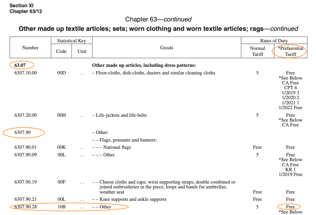
Regarding HS code and duty rate of face masks in some major countries, we collected some information in main trade partners (US, Japan, EU, Korea, Taiwan, Australia, New Zealand) of China. This is aimed at the face masks such as personal protective masks without special function components, including medical face masks and disposable face masks. All of below information were published by the custom officially.
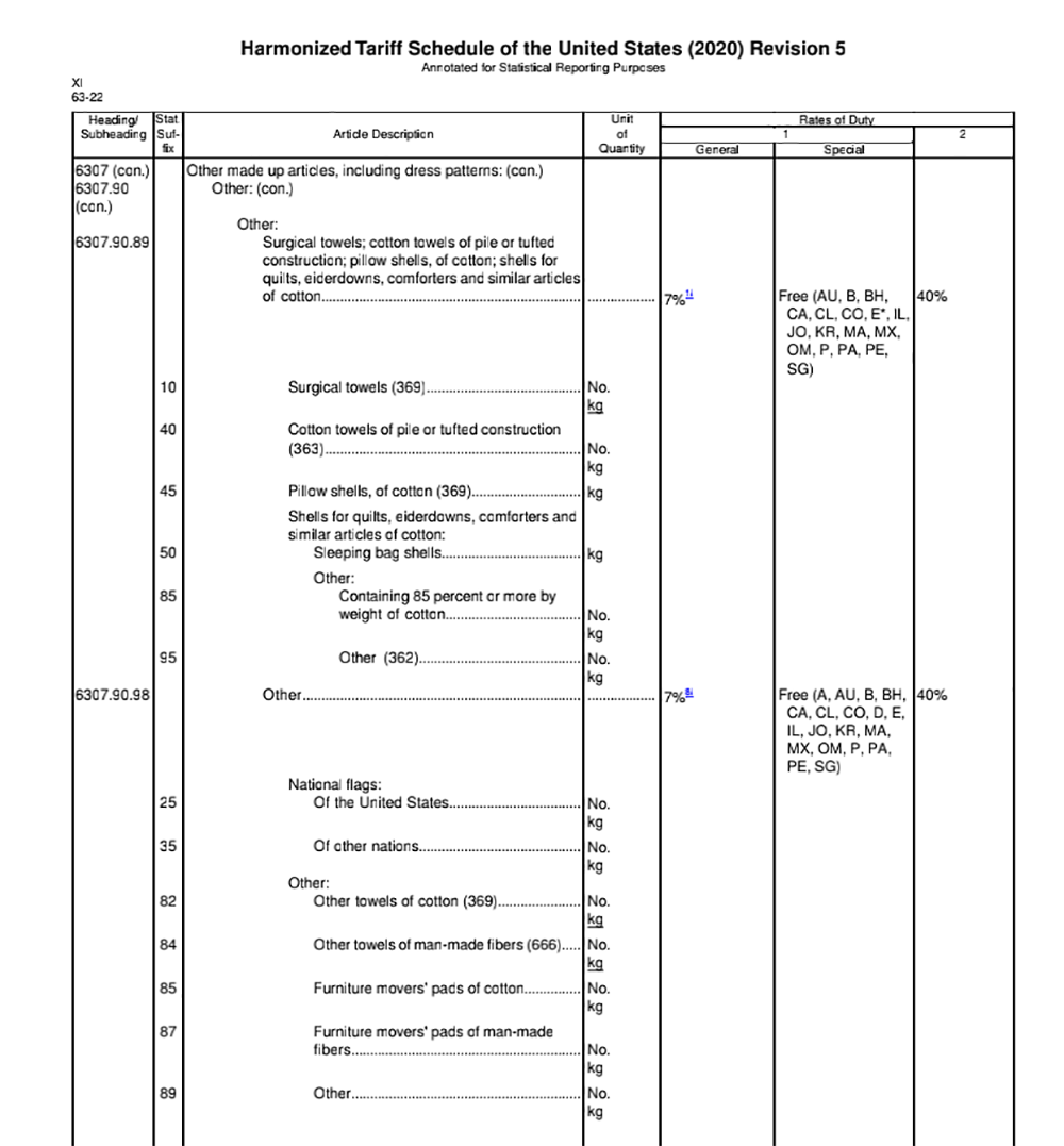
US:
According to Harmonized Tariff Schedule of the United States, HTSUS, the HS code of face masks in the US is 6307909889. And the duty rate imported from China is 7%. Regarding tariff imposed, according to announcement from the United States Trade Representative on March 12, 2020, the tariff is excluded for the face masks belonging to this HS code since September 1, 2019. Since then, all the face masks imported from China has been exempted from tariff. You can refer to the below chart for more information.
face mask tariff
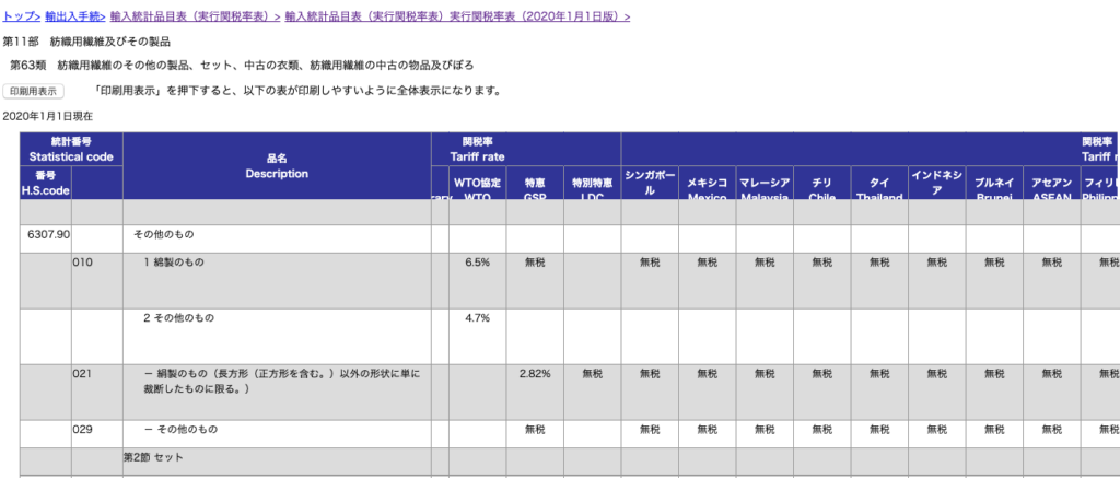
Japan:
The HS code of face masks in Japan is 630790029. The duty rate imported from China is 4.7%. To learn more, see below:
face mask tariff
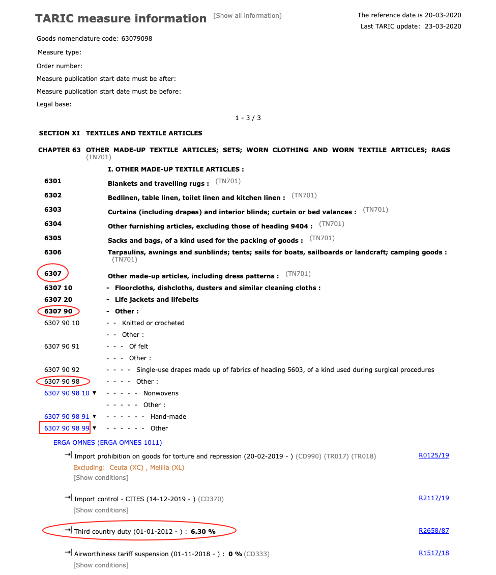
EU:
The duty paragraph for face masks imported from China in EU is 6307909899 and the duty rate is 6.3%. You can see below for more information:
face mask tariff
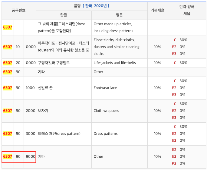
Korea:
The duty paragraph for face masks imported from China in Korea is 6307909000, and normally, the tariff is 10%. However, from March 18, 2020 to June 30, 2020, Korea has been suspending imposing tariff for face masks from China(0 tariff currently), see below for more information:
face mask tariff
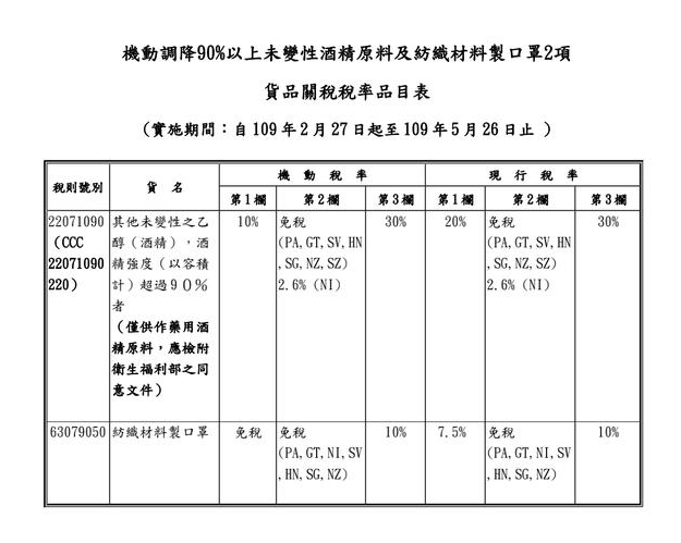
Taiwan, China:
The HS code(also referred to as duty paragraph) of face masks imported from China mainland in Taiwan is 63079050.
And, the duty rate for face masks imported from China mainland is 7.5%. However, from February 27, 2020 to May 26, 2020, provisional tax rates (also referred to as“flexible tax rateâ€in Taiwan area) for face masks was carried out in Taiwan area, i.e. the tariff is zero. You can see below for more information:
face mask tariff
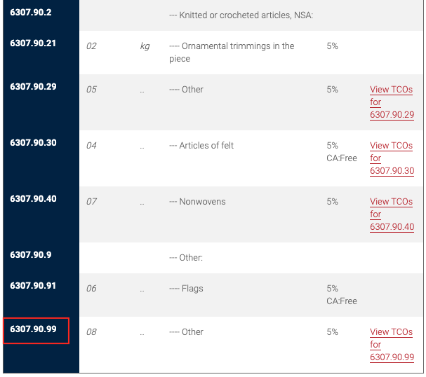
Australia:
The HS code of face masks imported from China in Australia is 63079099 and the duty rate is 5%. See below for more information:
face mask tariff
New Zealand:
The HS code of face masks imported from China in New Zealand is 63079028. Zero tariff is applied to the face masks imported from China according to “New free trade agreementâ€. See below for more information:
The abbreviations PWB and PCB are very common, especially in the field of electronics manufacturing. Therefore it is necessary to gain a clear understanding of the meaning of each one and the differences between the two. On this article, we will help our readers to distinguish PWB from PCB.
pcb vs pwb
PCB: Based on insulating substrate, it means a kind of products on which the wires are connected and components are printed from point to point on a dielectric substrate in a predetermined design. It is the English abbreviation of Printed Circuit Board.In a word, PCB stands for printed circuit board, where the width, side to side and multi-layer relationship(spacing) of conductor runs has or is designed to have a specific effect on circuit operation other than just a point to point connection.
PWB: Based on insulating substrate, it means a kind of products on which the wires are connected from point to point on a dielectric substrate in a predetermined design. However, there is no printed component on it. PWBs are the early name of the British, because at that time there were only circuit diagrams on the circuit board, but no printed components. So they belonged to the more primitive board. Under its effect, now many traditional British and some Hong Kong people still call the circuit board to be PWB, which is the English abbreviation of Printed Wire Board. In a word, PWB stands for printed wiring board, one of the first uses when the issue was only a point to point connection.
The PCBs are the boards already equipped with various components, however the PWB is just a designed substrate with no components.
pcb vs pwb
Moreover, PWB vs PCB greatly varies from one region to the other. For example, in the United States of America, the term Printed Circuit Board is more common in use while the use of the name PWB is more commonly used in Japan. In Japan, PWB is more preferred that PCB because it prevents confusion with another name, polychlorinated biphenyls, which refers to a particular poison available in Japan.
For your more information, in approximately 1999 the IPC Technical Activities Executive Committee made a mandate to only use the term PCB for all new document development because more often than not the printed circuitry design will have an impact on function.
If you are still confused or have any queries or comments about PCB, do not hesitate to contact us. Our sales team can give you a reply at our soonest convenience.