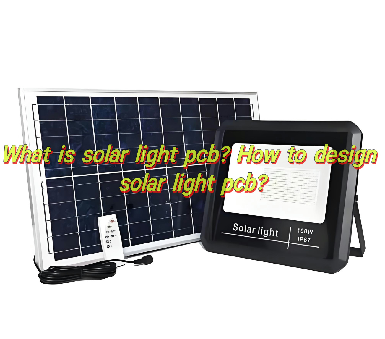
Solar light PCB plays a vital role in modern solar-powered lighting systems, allowing solar panels, batteries, and LED to work together smoothly. Whether it’s for street lighting, garden decoration, or night lamps, the right solar light PCB design helps the whole system run safely and efficiently. Many businesses and designers today focus on improving the performance of solar light PCB to make solar lighting smarter, more reliable, and longer-lasting.
At EBest Circuit (Best Technology), we specialize in solar light pcb solutions and PCBA services with fast delivery and affordable price. Feel free to contact us sales@bestpcbs.com if you have any request for solar light pcb.
Now, let’s explore the functions, benefits, materials, and design tips to help you better understand solar light PCB and how to make the right design choices.
What Is Solar Light PCB?
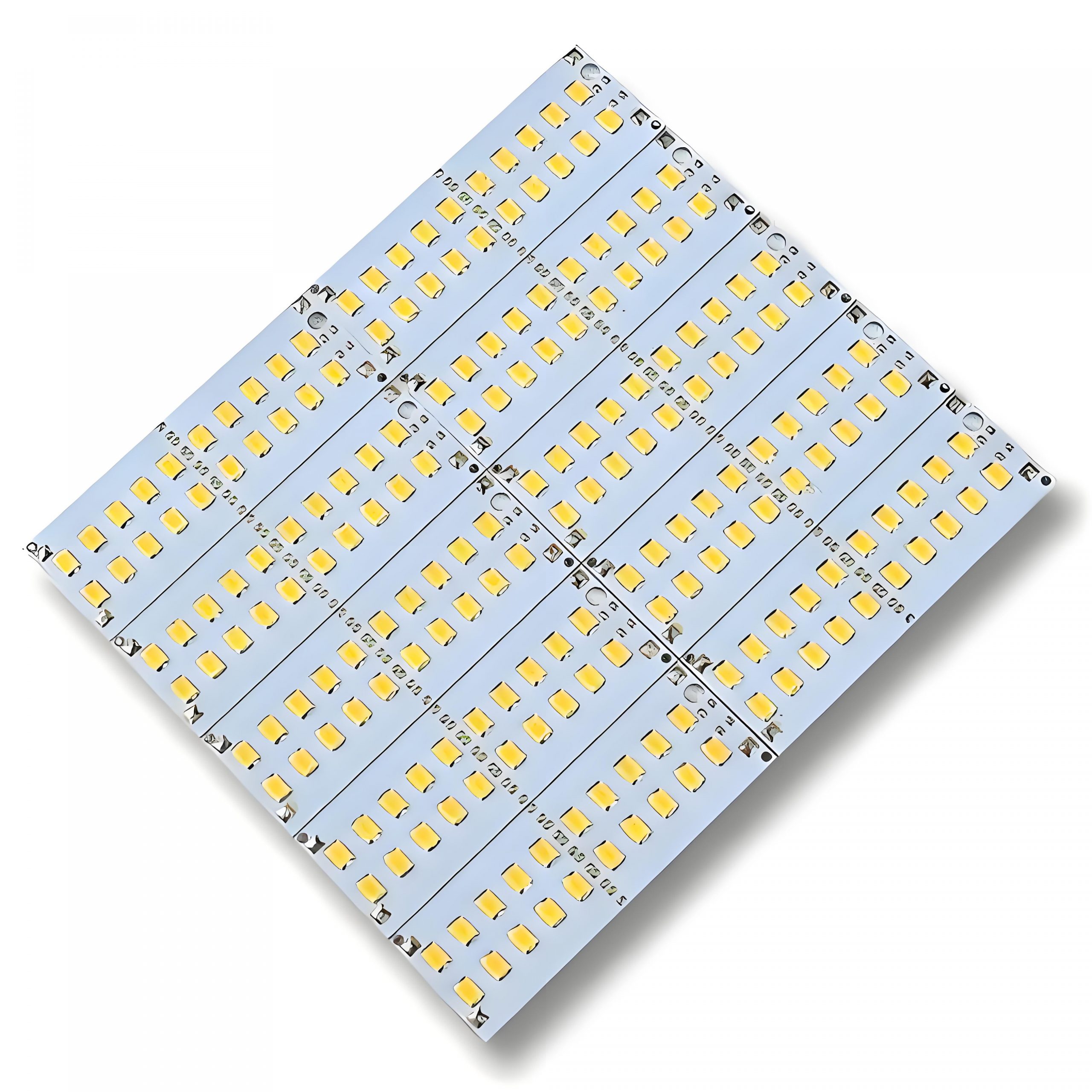
Solar light PCB refers to the printed circuit board used in solar lighting systems. These PCBs connect and support components like solar panels, batteries, charge controllers, LED drivers, and light sensors. Unlike regular PCBs used indoors, solar light PCB works outdoors, which means they must handle heat, moisture, and temperature changes.
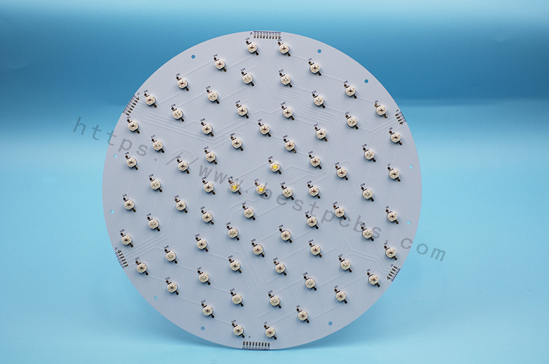
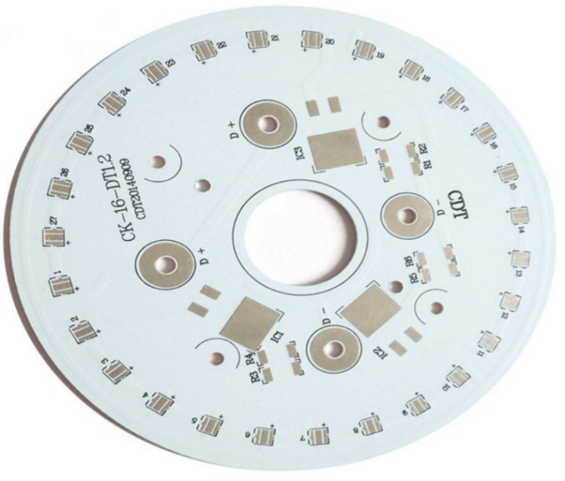
In most cases, solar light PCB comes in compact layouts to fit inside street light poles, garden light fixtures, or small night lamps. A good design helps solar panels collect energy during the day, store it in the battery, and smoothly light up the LEDs at night.
Compared to traditional PCB designs, solar light PCB pays more attention to energy conversion, power control, and long-term reliability. Since solar lighting focuses on low energy waste, the solar light PCB must also ensure minimal power loss during energy transfer and storage.
Advantages of Solar Light PCB Board
Here are advantages of solar light PCB board:
- Efficient energy conversion and integration
Optimized photoelectric conversion: Adopting high-transmittance substrate (such as FR-4 fiberglass board) and back-contact solar cell unit design, it can achieve up to 24% sunlight conversion efficiency and significantly improve energy utilization.
Simplified circuit integration: Directly integrate solar cells and drive circuits through PCB process, reduce external cable connections, reduce losses and improve system reliability.
- Compact and lightweight structure
Lightweight and portable: Using flexible substrates (such as polyimide or PET) for PCB design, the thickness can be less than 1.6mm, which is suitable for miniaturized devices and complex installation scenarios.
High-density layout: Supporting micro components of 0402/0603 packages, combined with multi-layer wiring technology, greatly reducing PCB area.
- Environmental adaptability and durability
Weather protection: FR4 substrate with black solder mask ink has excellent UV resistance, high temperature resistance (up to 260°C) and moisture resistance, and can adapt to extreme outdoor climates.
Dynamic optimization capability: Integrated photoresistors and dynamic tracking algorithms adjust the angle of solar panels or charging strategies in real time to improve energy capture efficiency under weak light conditions.
- Cost-effectiveness and scalability
Low mass production cost: Standardized PCB production processes (such as SMT patches) support batch manufacturing, and the cost per unit can be reduced to less than US$0.05, which is significantly economical.
Modular design: Reserved interfaces support battery expansion (such as 2600mAh lithium battery) or function expansion (such as Wi-Fi module), which facilitates product iteration and upgrade.
- Environmental protection and sustainability
Recyclable materials: Compliant RoHS lead-free solder and epoxy resin substrates reduce environmental pollution and meet green manufacturing standards.
Energy self-sufficiency: Reduce dependence on traditional power grids through solar power supply systems, suitable for remote areas or scenarios without power grid coverage.
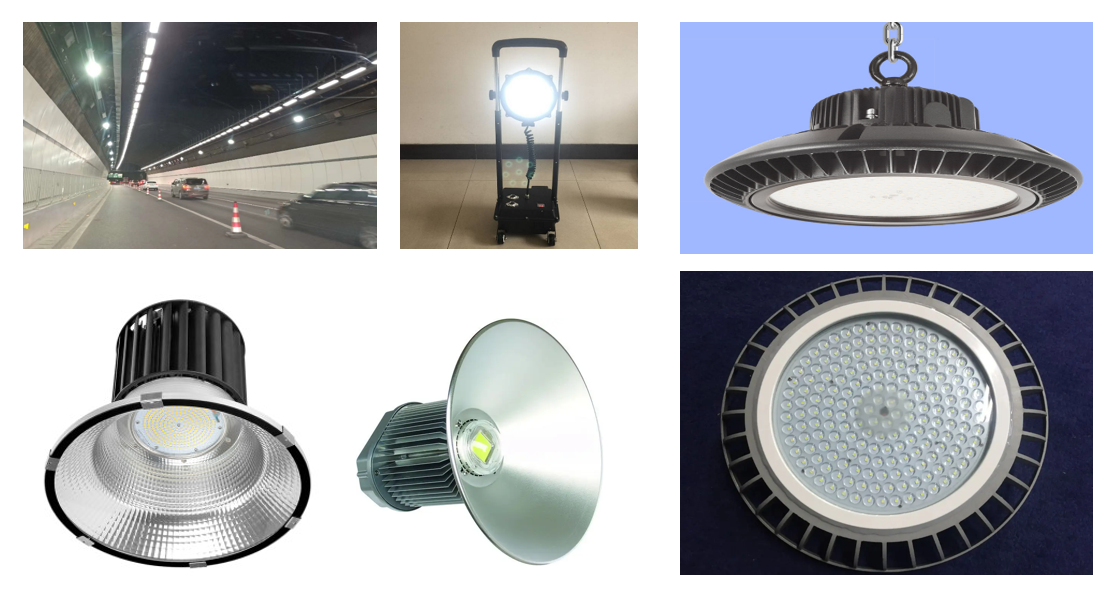
Application of Solar Light PCB Board
Solar light PCB Board power many outdoor and indoor systems:
- Street lighting in rural, urban, or off-grid areas.
- Garden lighting for decorative or functional purposes.
- Pathway and driveway lights to improve safety and visibility.
- Fence and wall lights to highlight property boundaries.
- Camping lights for portable, off-grid use.
- Emergency backup lights for disaster situations.
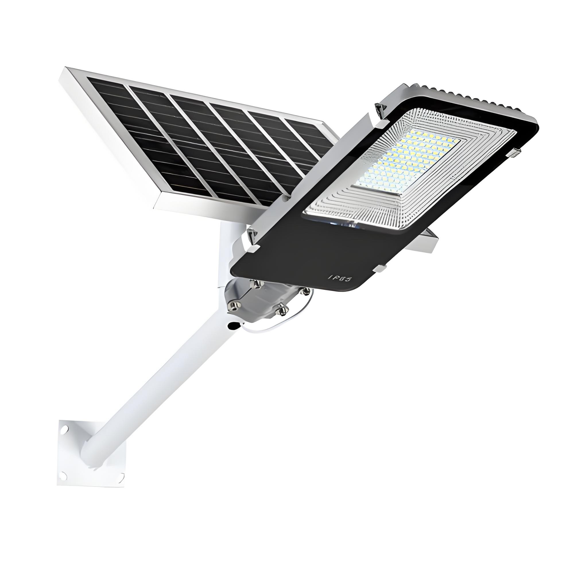
These boards fit many settings, offering clean energy solutions where traditional power is limited or expensive.
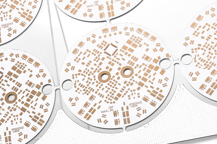
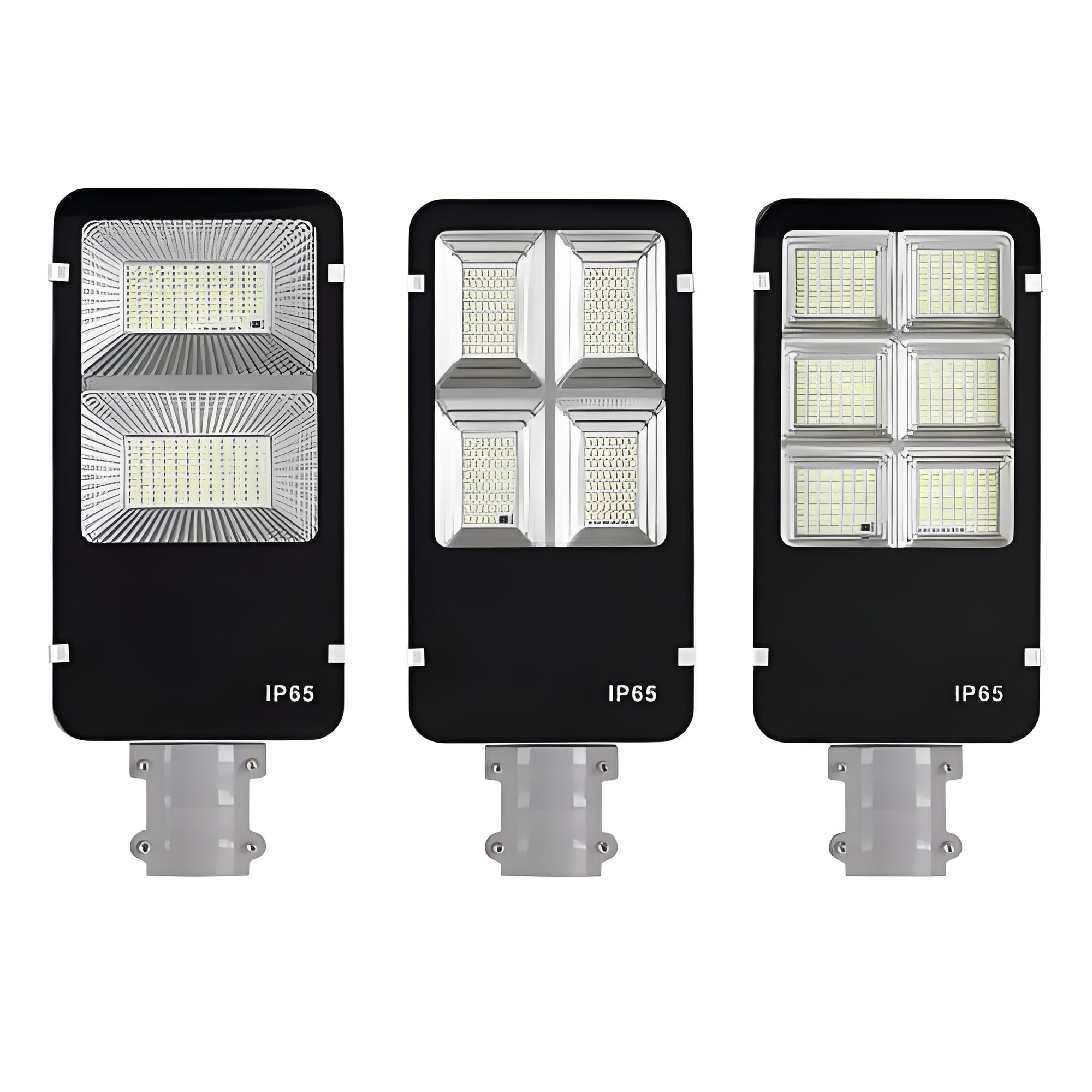
What Are Types of Solar Light PCB?
The types of solar light PCB can be divided based on its structure and function. Here are a few common types you’ll see:
- Single-sided PCB
This type has all copper traces on one side. It’s commonly used in simple solar lights, especially garden or pathway lights. The cost is lower, but it works well for basic circuits.
- Double-sided PCB
For more complex designs, solar light PCB can have copper traces on both sides. This allows more connections and better space usage. Many solar street light PCB boards use this type to handle multiple components in limited space.
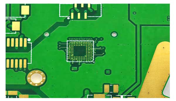
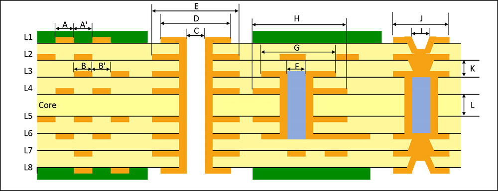
- Multi-layer PCB
It contains multiple conductive layers and insulating layers, and is electrically connected through internal vias, suitable for highly integrated and complex circuits.
The Best PCB Manufacturer of Solar Light PCB-EBest Circuit (Best Technology)
Choosing the right solar light PCB manufacturer matters as much as the design itself. At EBest Circuit (Best Technology), we specialize in producing high quality solar light PCB board for different solar lighting applications. With over 18 years of experience, our team understands the unique needs of solar projects, from small garden lights to large street lighting systems.
Our factory supports custom designs, fast prototyping, and reliable production for solar street light PCB, solar garden light PCB, and other types of solar lighting boards. We also focus on quality, using top materials and strict testing processes to deliver durable boards that perform well outdoors.
Besides product quality, EBest Circuit (Best Technology) offers professional technical support, helping customers turn their ideas into real products with the right solar light PCB design. Whether you’re building smart street lights or decorative garden systems, we can be your trusted partner in PCB manufacturing.
Materials of Solar Light PCB Board
The materials of solar lamp PCB mainly include the following types, which are based on the requirements of different application scenarios and production processes:
- Substrate material
FR-4 fiberglass board: It is made of glass fiber cloth and epoxy resin laminated together, with good mechanical strength, high temperature resistance and insulation, and is the mainstream PCB substrate choice.
PET laminate: Some solar lamp PCBs use polyethylene terephthalate (PET) as the base plate, which is often used in lightweight or flexible circuit demand scenarios5.
- Conductive layer material
Copper foil: As the core material of the PCB conductive path, it forms the circuit pattern through the etching process to ensure the stability of current transmission (conventional materials are not directly quoted, but are common in the industry).
- Solder mask and protective materials
Black solder mask ink: It is used for surface covering to prevent oxidation and short circuit, and has high temperature resistance. It is commonly used in automotive electronics or outdoor equipment.
Fireproof material: Such as 22F fireproof grade material, which enhances the safety of PCB in high temperature environment
- Special functional materials
Insulating resin (epoxy resin): used for inter-layer bonding and insulation protection, improving the stability and weather resistance of the overall structure.
Wear-resistant laminated cloth: adding a wear-resistant layer to the surface of some fiberglass boards to extend the service life of PCBs in complex environments.
- Auxiliary component integration materials
Semiconductor materials (such as silicon-based components): integrating TP4056 charging IC, Mosfets driver chip, etc., for battery management and light control function realization.
How to Design Your Solar Light PCB?
Designing a solar light PCB involves several clear steps:
Step 1: Define Your Solar Light’s Needs
Before starting the actual PCB layout, understand your product’s needs. Is it a solar street light with high power LEDs? Or a solar garden light that needs a small, simple circuit? Defining power levels, light brightness, battery size, and working time helps choose the right parts and board type. Outdoor products often face heat, moisture, and dust, so all these need to be considered from the start.
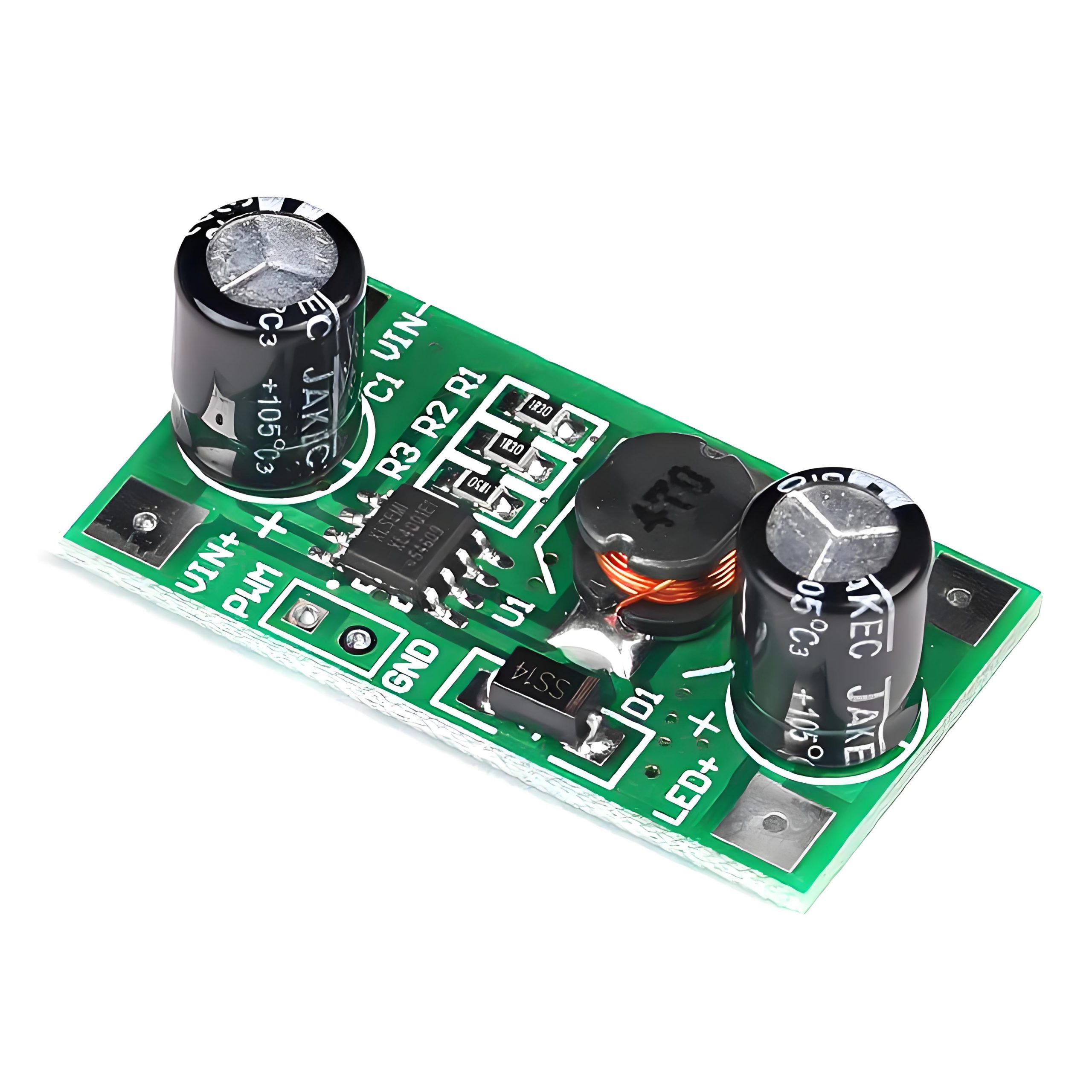
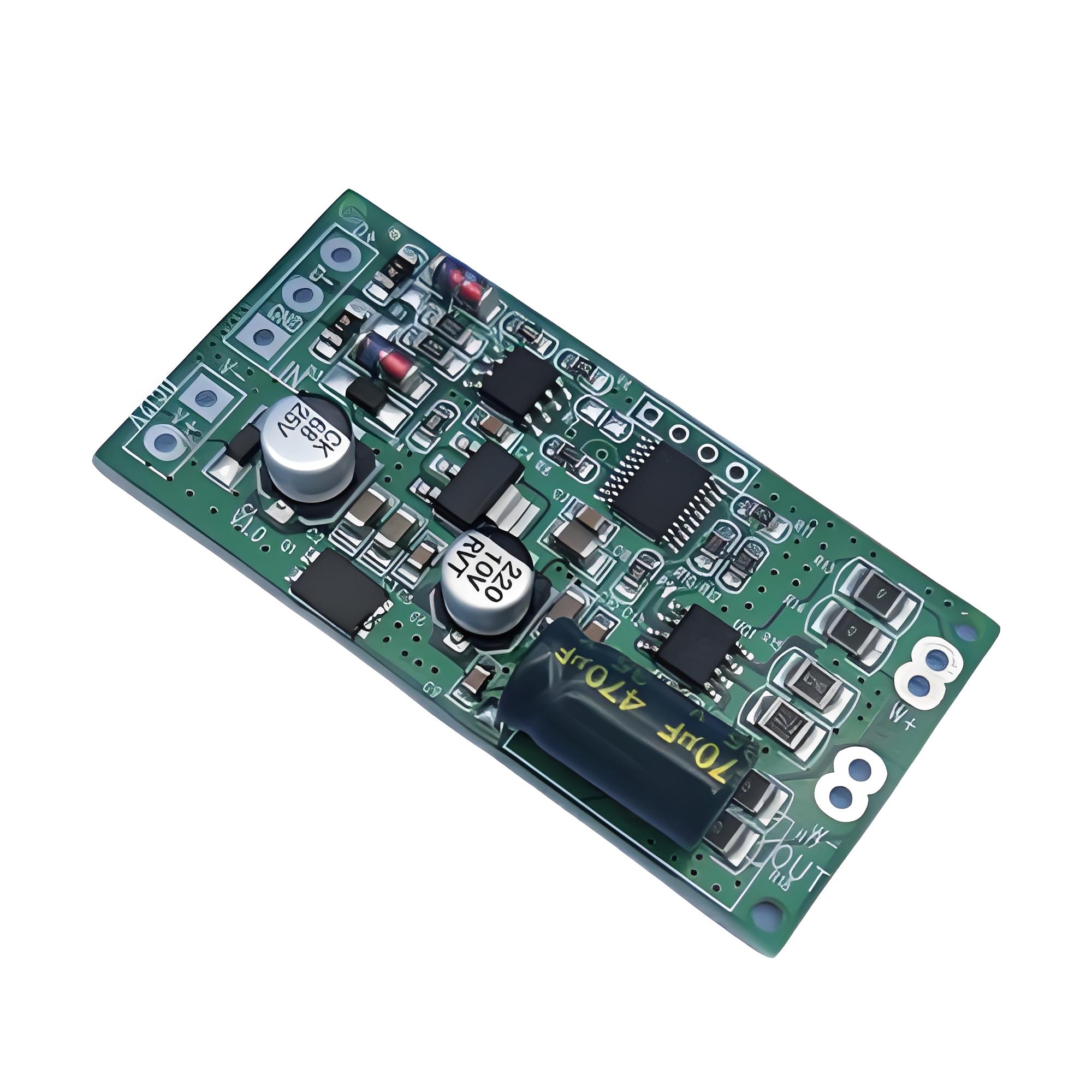
Step 2: Choose the Right PCB Type
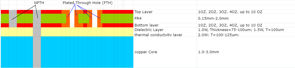
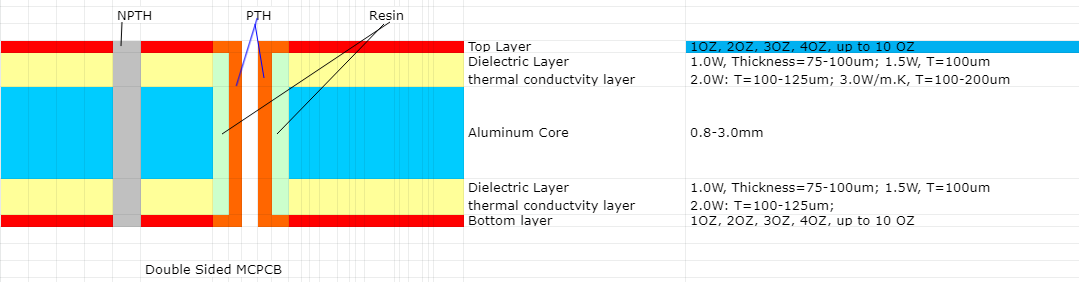
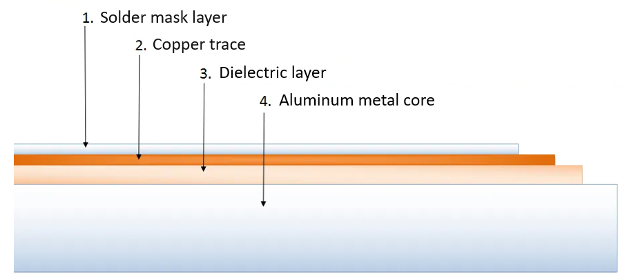
Different solar lights need different board types. For solar street lights, heat control is critical. That’s why aluminum PCB or metal core PCB works better. For small solar night lights, flexible PCB can fit tight spaces. Choosing the right board helps your solar light PCB last longer while keeping costs under control.
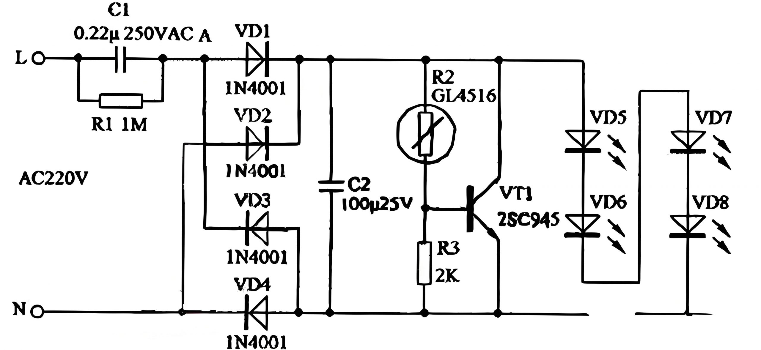
Step 3: Create the Circuit Diagram
A clear solar street light circuit diagram helps guide the whole process. It shows how the solar panel, battery, LED driver, light sensor, and controller connect. This step is where you check voltage levels, current flow, and safety protections. A simple mistake here could cause power loss or shorten battery life. Keep it simple but cover every important part.
Step 4: Component Placement Planning
Next, think about where each part goes. Solar lights often use light sensors and charging controllers. These parts should sit close to each other for better signal control. LEDs usually sit on the outer edges, especially for solar street light PCB boards, where wide light coverage matters. Placing parts correctly helps with heat flow, power management, and even future repairs.
Step 5: Trace Routing and Power Paths
Good trace routing makes sure power flows smoothly across your solar light PCB board. High power traces, like those from the solar panel to the battery, need to be wide enough to handle current without heating up. Signal traces, like those from the light sensor to the controller, should stay short to avoid interference. Keeping power and signal paths separate reduces noise and helps the whole system work better.
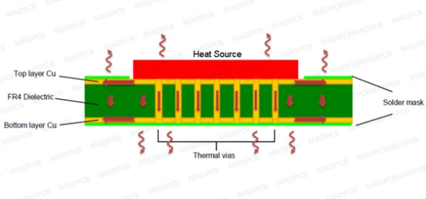
Step 6: Thermal Management Planning
Outdoor solar lights face direct sunlight, so heat control is important. For solar garden light PCB boards and solar street light PCB boards, adding thermal vias or using a metal core PCB can pull heat away from sensitive parts. Placing heat-producing parts, like LED drivers, away from the battery extends battery life too. Good heat management helps prevent early failures.
Step 7: Waterproofing and Protection
Most solar light PCB boards work outside, so water and dust protection is critical. Adding conformal coating or waterproof housings helps protect the board. Using corrosion-resistant materials for connectors and ensuring the PCB edges are sealed also improves reliability. These steps help your solar light PCB last longer in all weather conditions.
Step 8: Battery Charging and Protection Circuits
A solar light isn’t just about lights and sensors. The battery charging circuit plays a huge role in the whole system. Overcharging, deep discharge, or uneven charging can shorten battery life. Adding smart charge controllers helps balance charging and discharging cycles. Including reverse polarity protection also prevents accidental damage during assembly.
Step 9: Light Sensor and Control Integration
To make your solar light smarter, the light sensor must work well with the controller. For solar night light PCBs, light sensors control when the lights turn on and off. Proper sensor placement, away from shadows or light reflections, makes the system more reliable. Adding software controls for dimming or timing also adds value, especially for solar street light PCB boards.
Step 10: Testing and Prototyping
Before moving to full production, testing the first solar light PCB board is critical. Check power flow, battery charging, light sensing, and LED brightness under real outdoor conditions. Testing in both sunny and cloudy weather helps make sure the light works well all year. Making small changes to improve power efficiency or adjust sensor sensitivity at this stage helps avoid bigger problems later.
Step 11: Cost Control and Material Choice
While design quality matters most, keeping costs under control helps stay competitive. Choosing the right substrate — FR4, aluminum, or ceramic — balances performance and cost. Picking components with good lifetime ratings but fair prices also helps. For solar street light PCB boards, spending more on heat-resistant parts pays off in the long run.
Step 12: Partner with a Reliable Manufacturer
Even the best design won’t work well if the manufacturing process isn’t strong. Working with a reliable solar light PCB manufacturer helps avoid common problems like uneven soldering, poor copper adhesion, or inconsistent coatings. A good partner can also suggest small improvements to make your design easier to produce or more durable outdoors.
To sum up, it’s very important to design the right solar light PCB to ensures smoother performance and fewer failures down the road. Likewise, it is equally important to choose a good solar light PCB supplier. Best technology would be a good choice for providing you with high quality solar light pcb solutions.
Conclusion
Last but not the least, the solar light PCB brings clean, reliable lighting to homes, streets, and gardens. With careful selection, proper design, and regular maintenance, these boards offer long-term service with minimal cost. Whether you need a solar street light PCB board or a solar garden light PCB, following these tips helps you create strong, efficient solutions tailored to different settings.