Would you like to know how to get a good price with high quality LED Panel PCB? Let’s explore more about LED panel PCB’s material, application, cost reduction solution and how to select a LED company.
EBest Circuit (Best Technology), we specialize in LED Panel PCB design and manufacturing over 18 years. We uses a fully automated SMT patch production line and AOI/X-ray inspection system, and has imported YAMAHA patch machines to ensure that the LED Panel PCB patch accuracy can reach ±0.035mm, and the mounting speed can reach 95,000 points/h. Based on the 30W+ high-power heat dissipation requirements, the design end can customize the 2oz copper substrate stack and honeycomb thermal conductive hole structure, and the measured full-load temperature rise is controlled within 12°C. Supports 15-day standard delivery and 7-day expedited delivery. If you have any request for LED Panel PCB, welcome to contact us: sales@bestpcbs.com
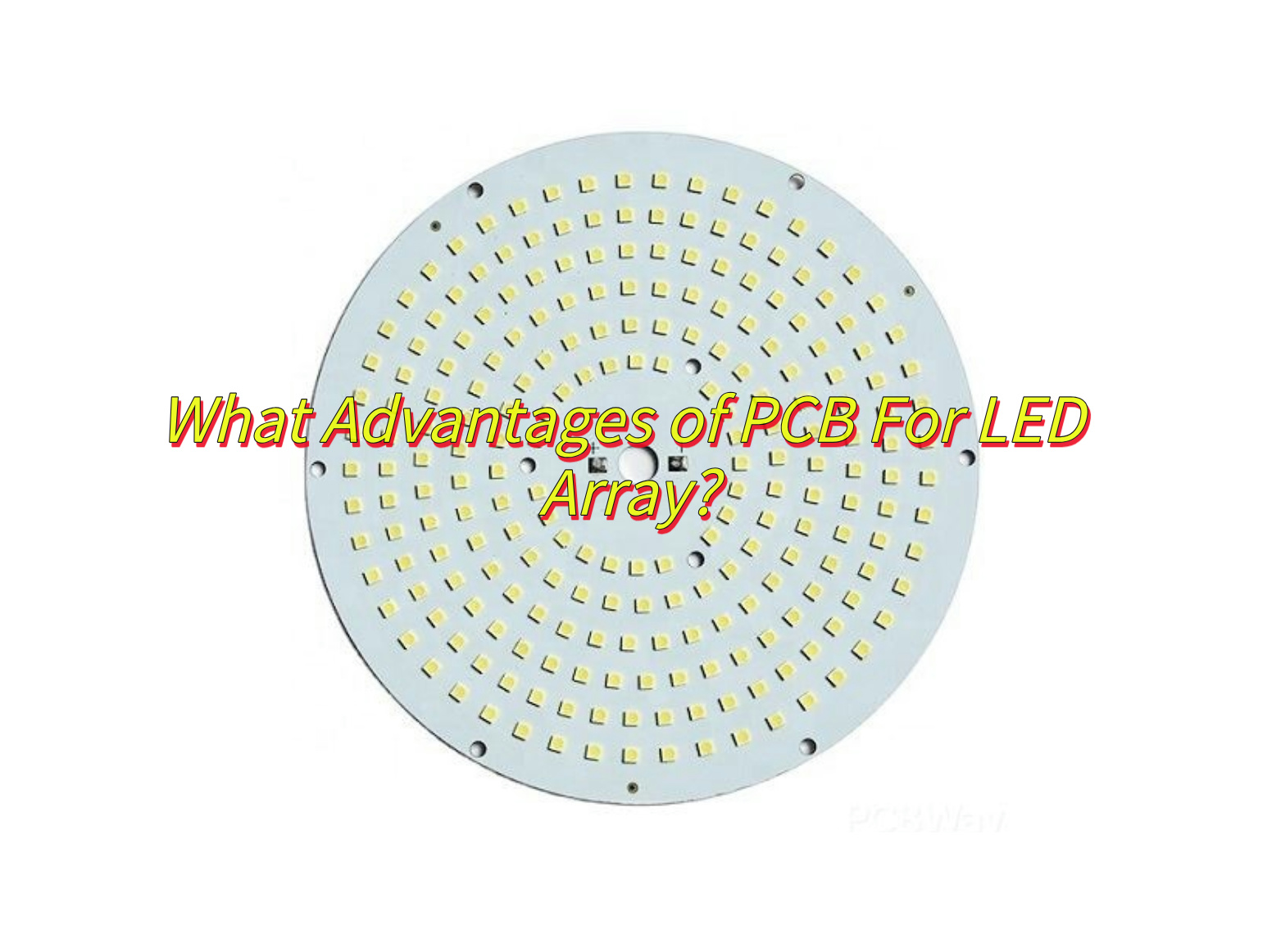
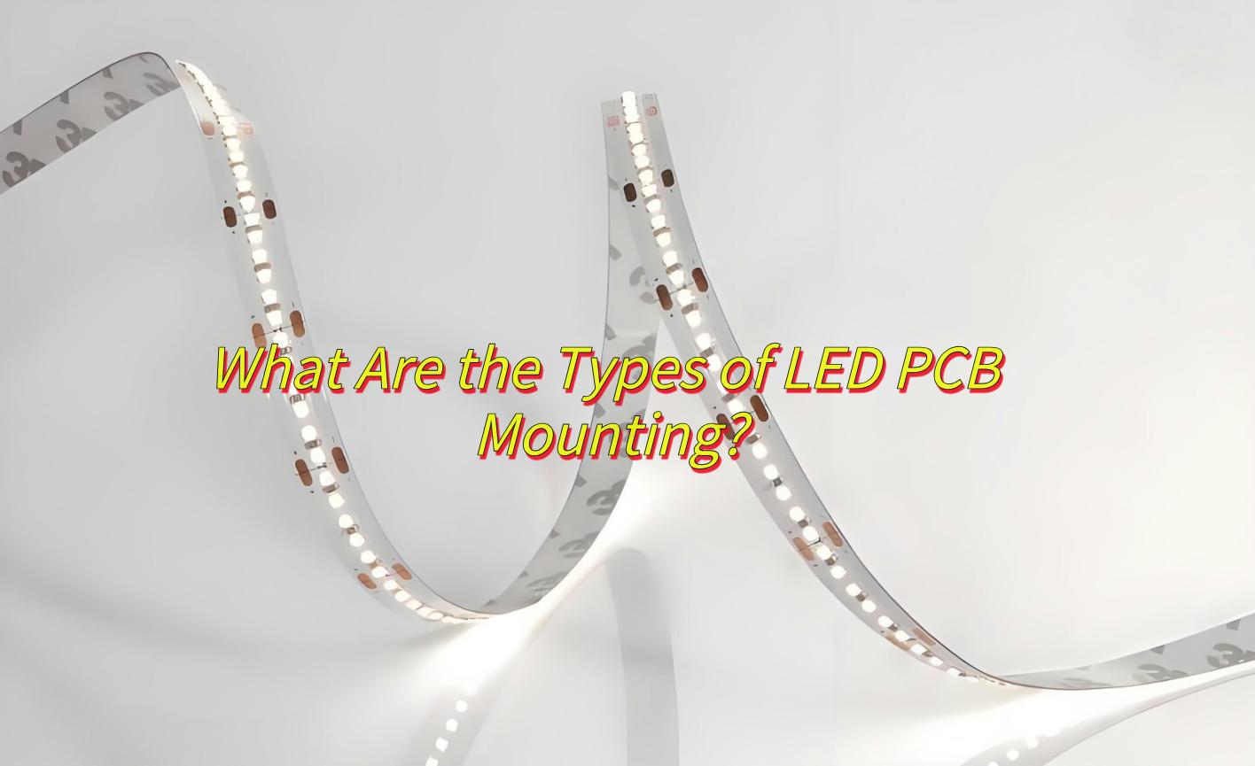
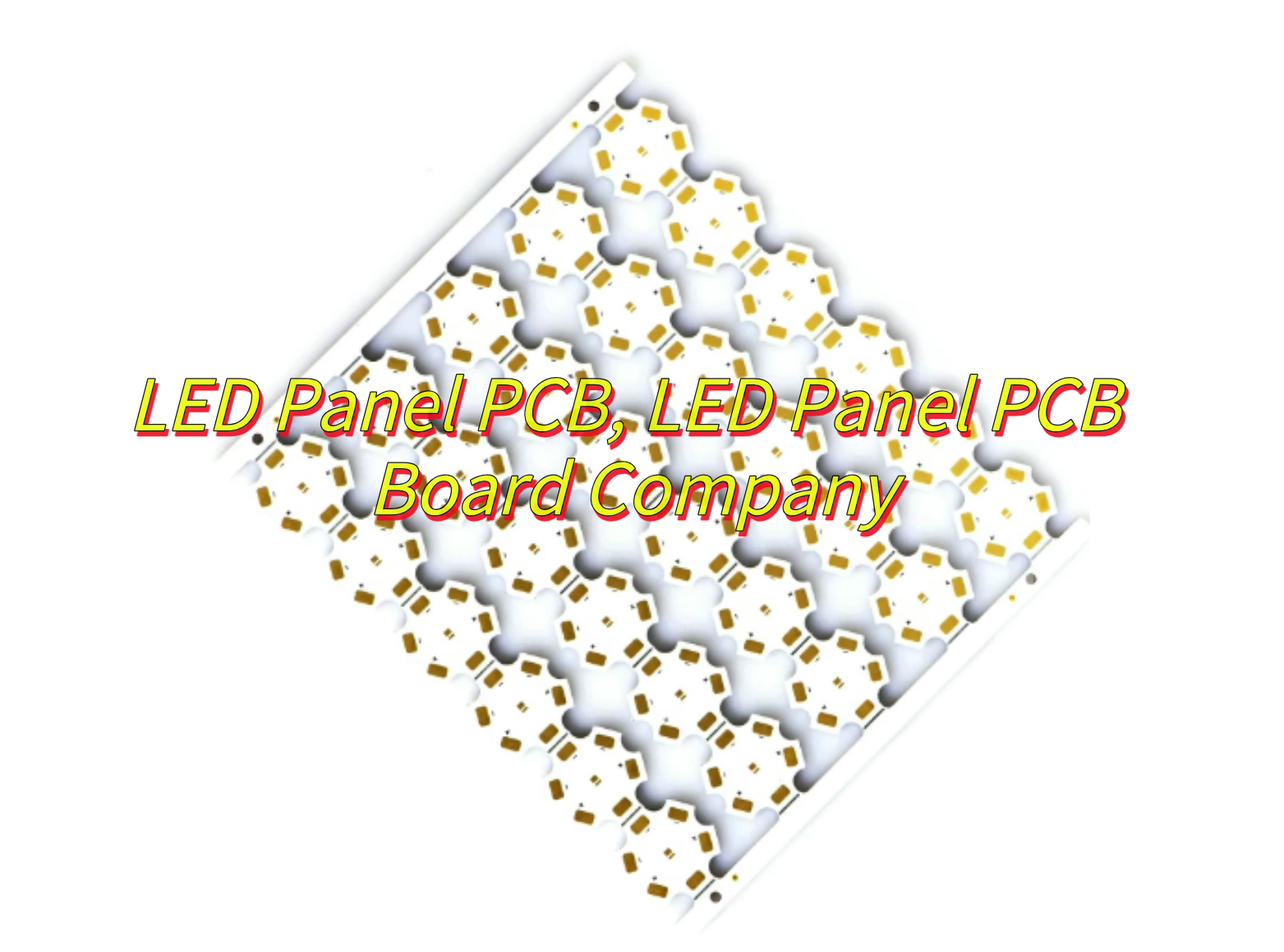
What Is LED Panel PCB?
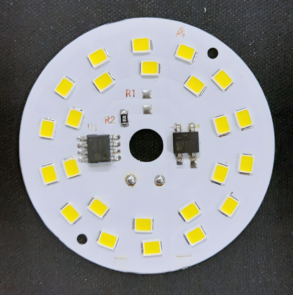
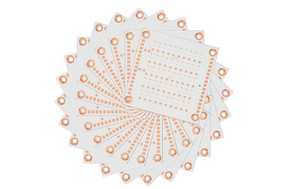
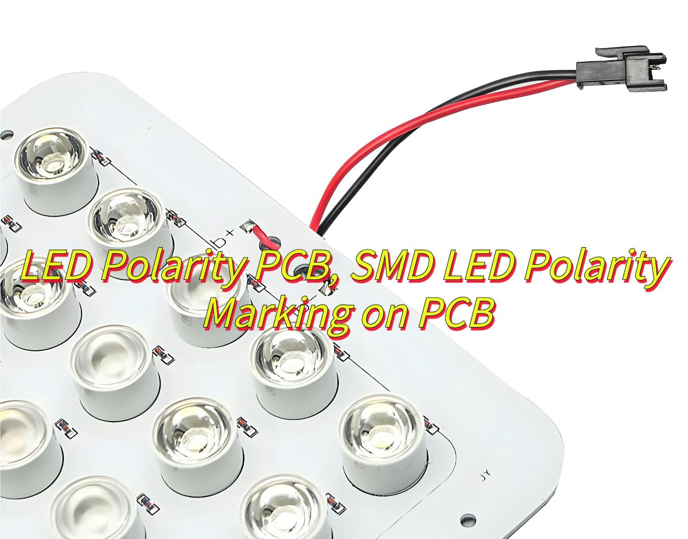
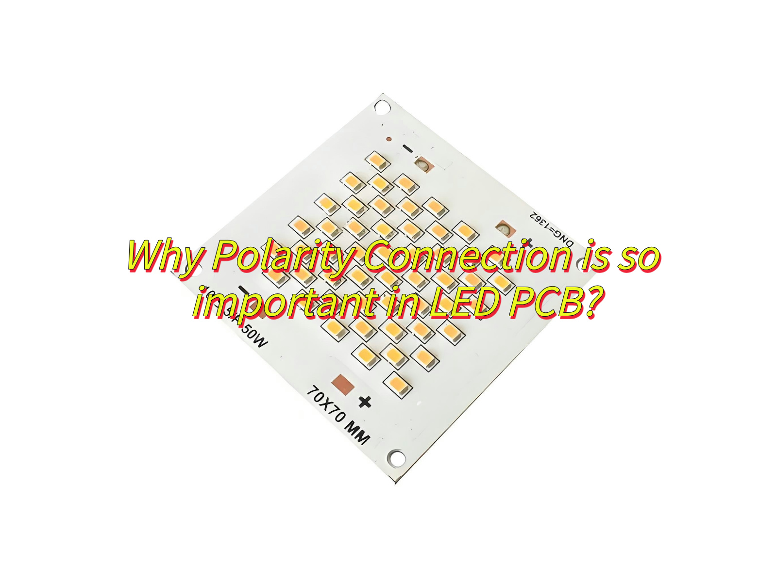
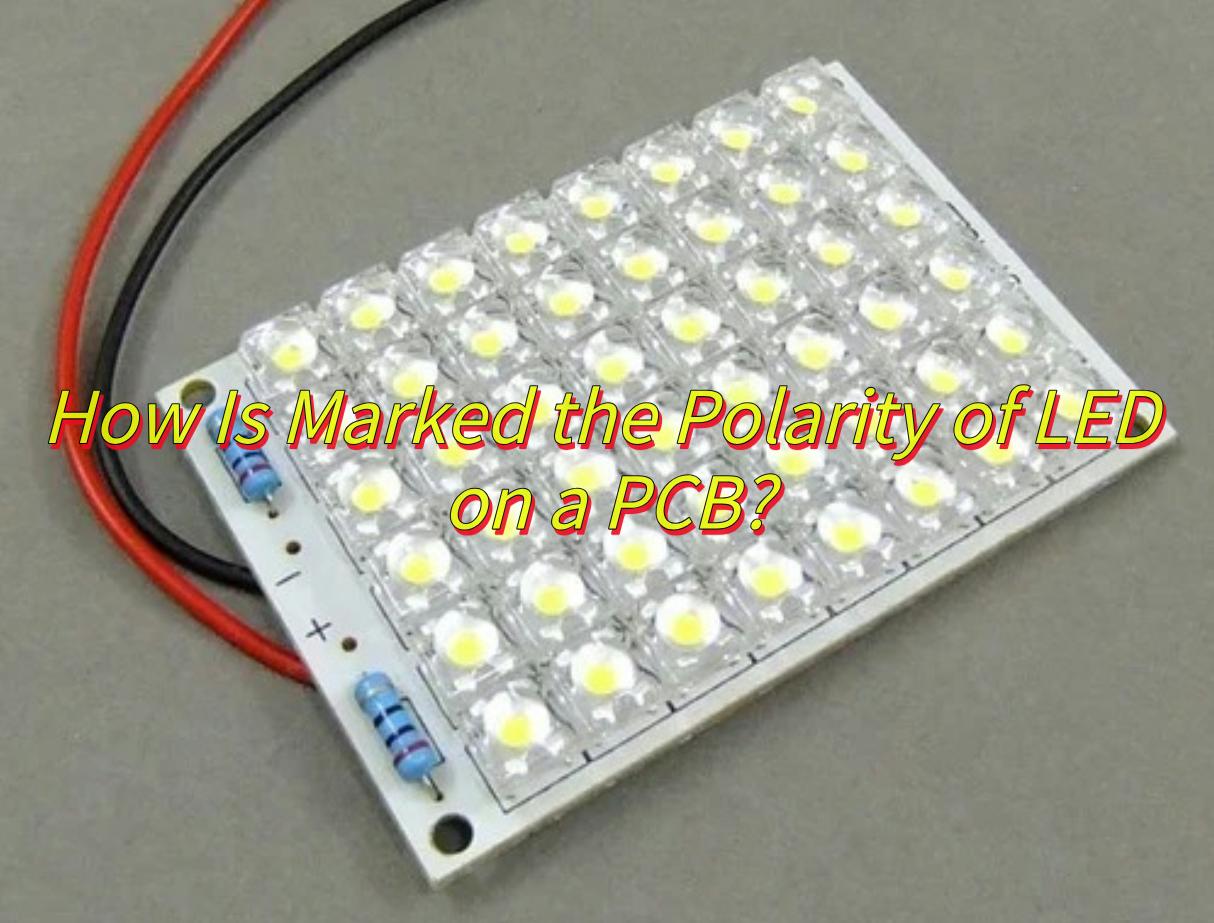
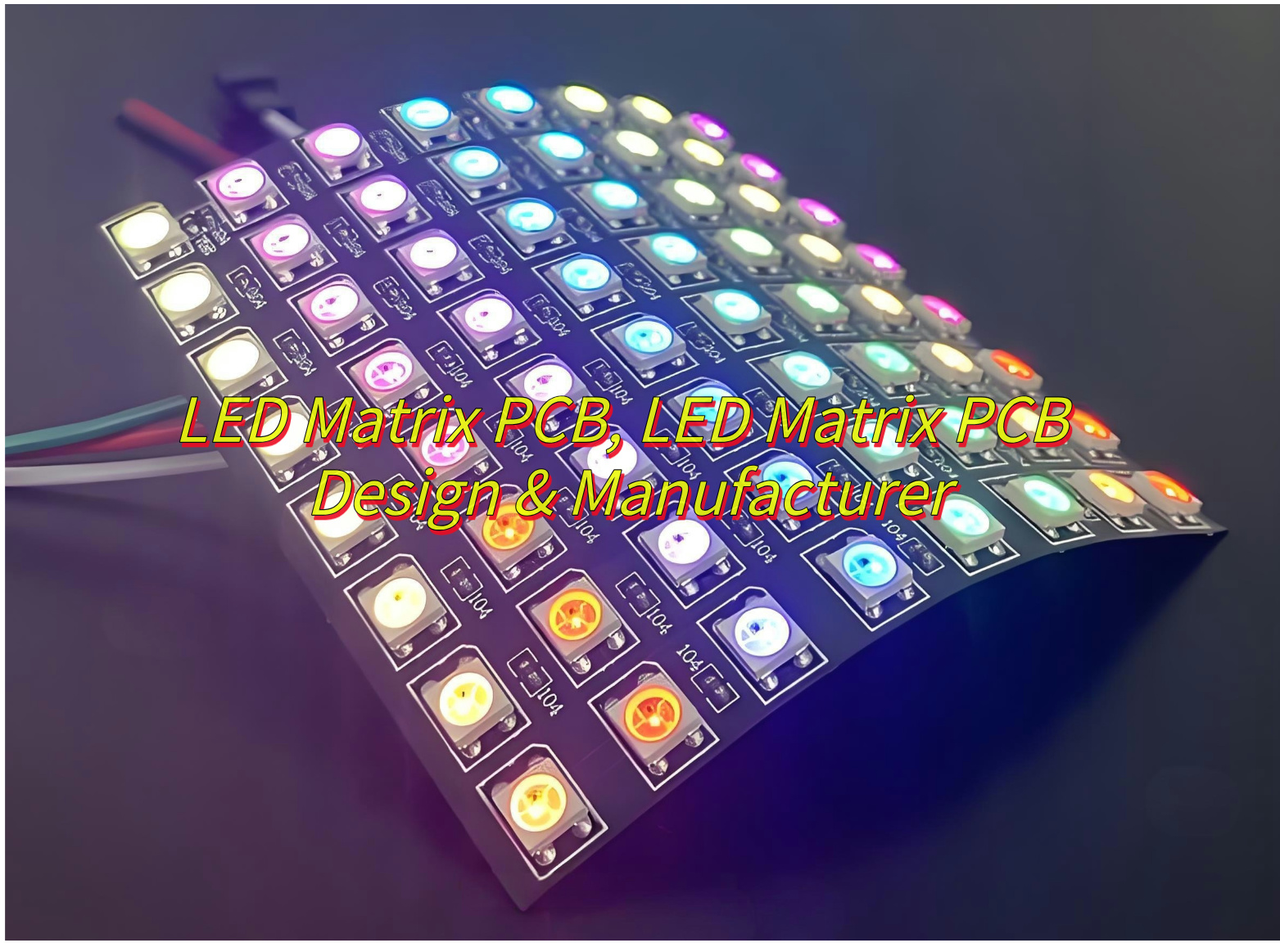
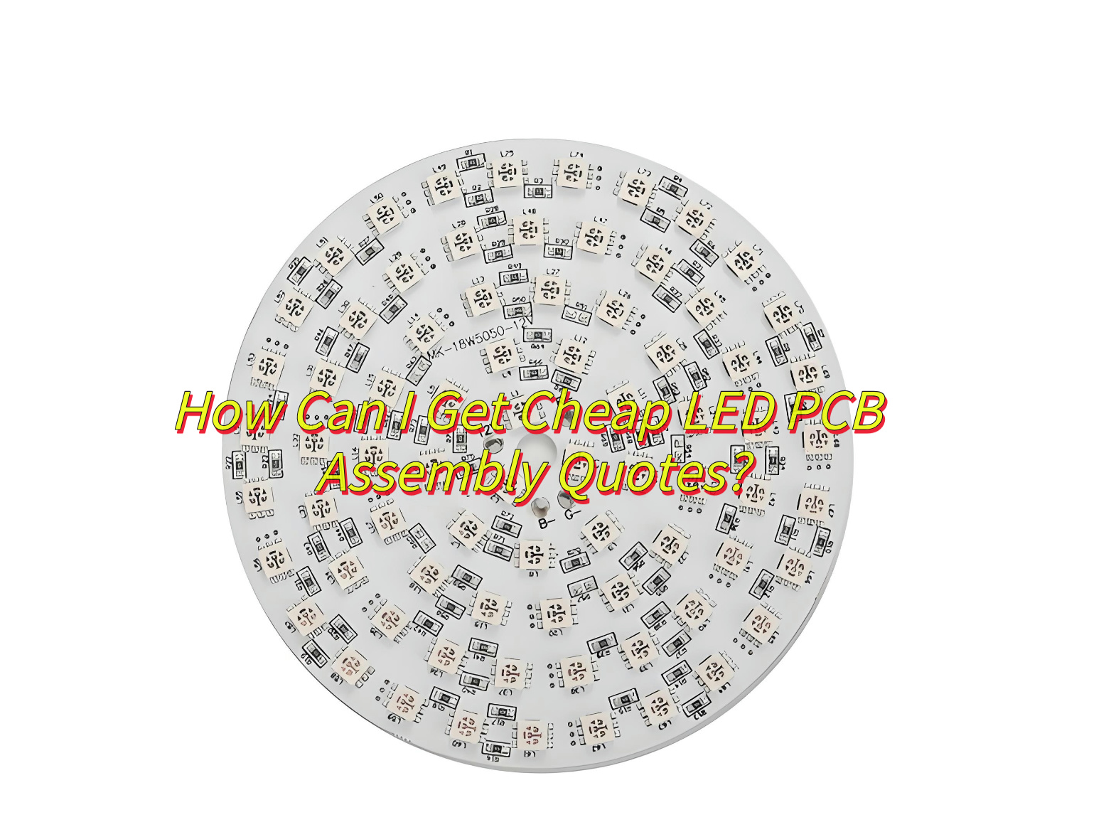
An LED Panel PCB is a specialized circuit board designed to power and control densely arranged LED arrays in applications like displays, signage, or lighting systems. These PCBs integrate high-current traces, driver ICs (e.g., TLC5940, WS2812), and thermal management features (vias, metal cores) to handle heat from prolonged LED operation. They often use aluminum substrates (for heat dissipation) or FR-4 with enhanced copper layers (for signal integrity), supporting configurations like COB (Chip-on-Board) LEDs or SMD modules. Key features include precise polarity marking (dots, notches) to prevent reverse connections, uniform voltage distribution, and EMI shielding for stable performance in automotive dashboards, retail displays, or architectural lighting. EBest Circuit (Best Technology) manufactures LED Panel PCBs with <0.1mm alignment tolerances, ensuring seamless LED array integration and longevity under high-brightness demands.
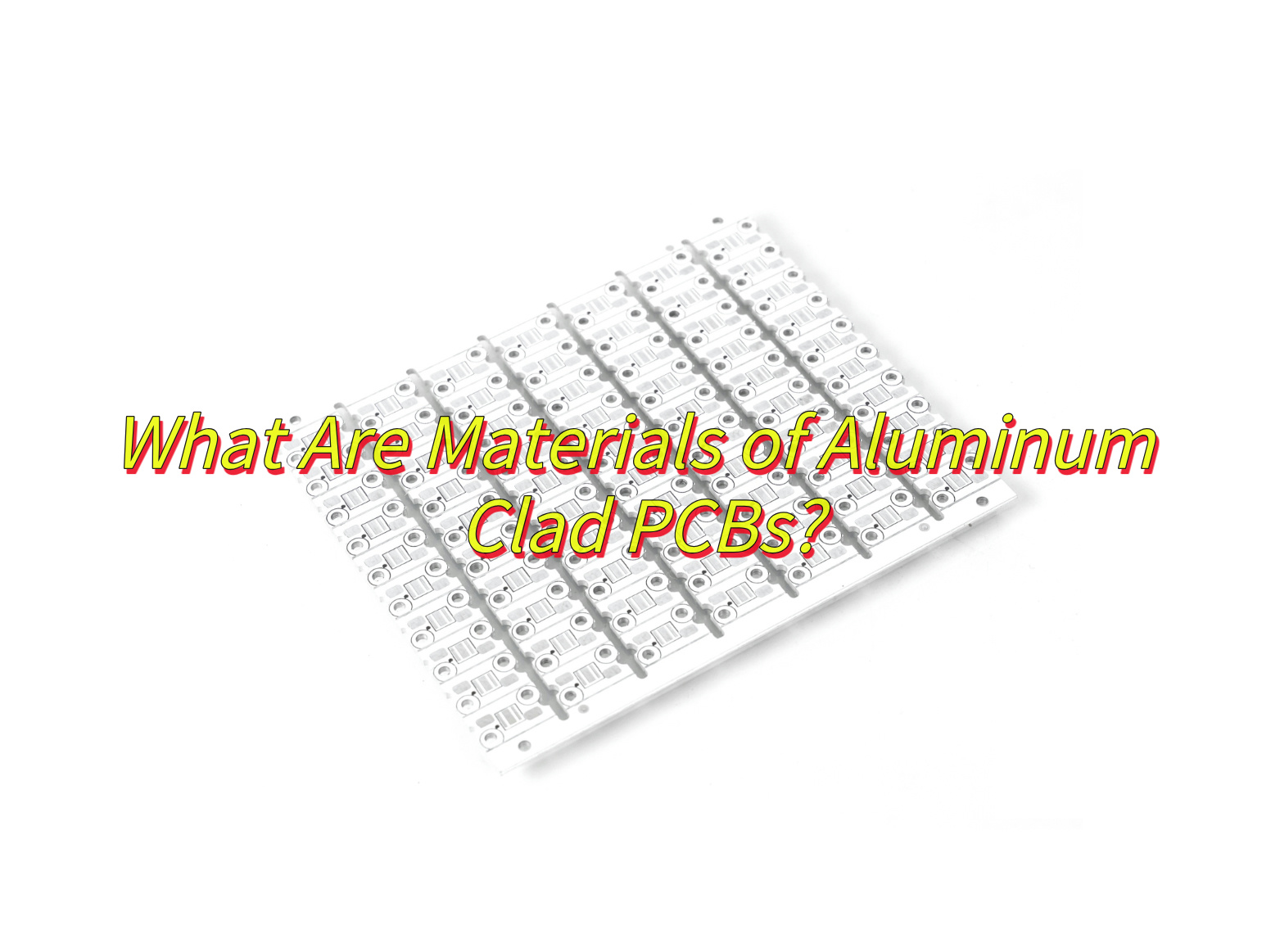
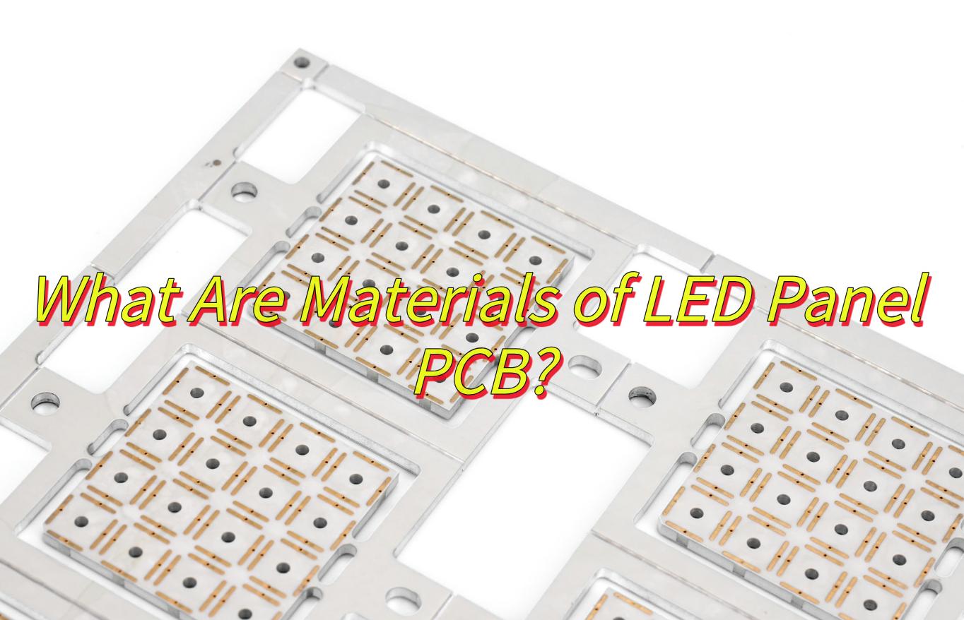
What Are Materials of LED Panel PCB?
Here are materials analysis of LED Panel PCB:
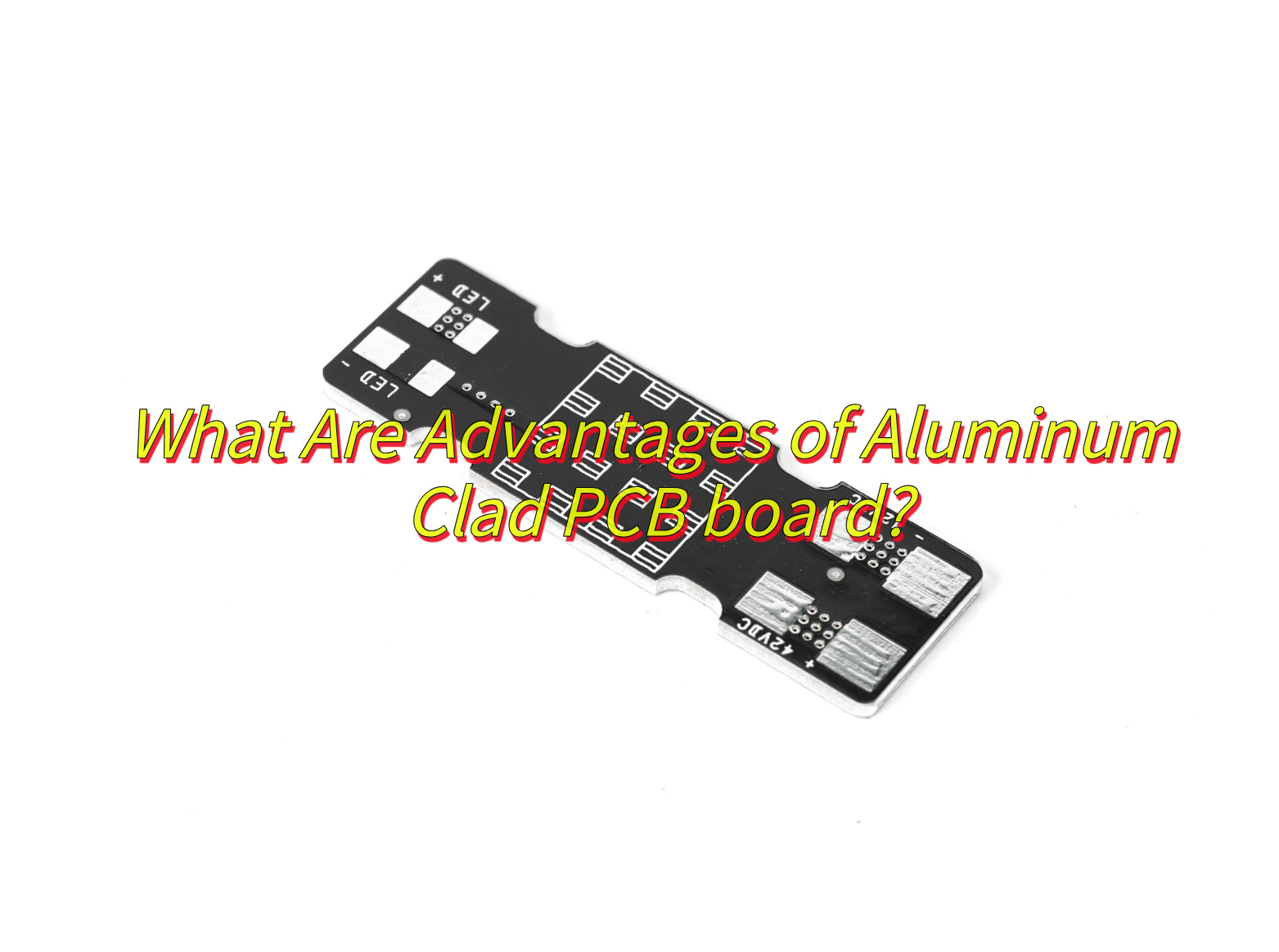
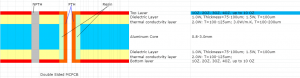
Aluminum Substrates (Best for High-Power/Thermal Management)
- Why Choose It: Offers superior heat dissipation, crucial for preventing LED overheating and extending lifespan.
- Ideal For: High-brightness LED panels, outdoor displays, automotive lighting, or applications where thermal performance is critical.
- Pros: Lightweight, durable, reduces the need for external heat sinks, and supports high-current designs.
- Cons: More expensive than FR-4 and less suitable for complex multi-layer designs.
FR-4 (Best for General/Low-Power Applications)
- Why Choose It: Cost-effective and widely available, making it ideal for indoor LED panels, signage, or consumer electronics.
- Ideal For: Basic lighting, low-brightness displays, or projects where heat generation is minimal.
- Pros: Easy to manufacture, supports 2–4 layers, and works well with standard SMT assembly processes.
- Cons: Poor thermal conductivity compared to aluminum; may require additional cooling for high-power LEDs.
Ceramic Substrates (Specialized Use)
- Why Choose It: Exceptional thermal and electrical insulation, suitable for high-frequency or high-temperature LEDs.
- Ideal For: Aerospace, military, or automotive applications requiring extreme reliability.
- Pros: High thermal conductivity, low CTE mismatch with LED components.
- Cons: Expensive, brittle, and difficult to process.
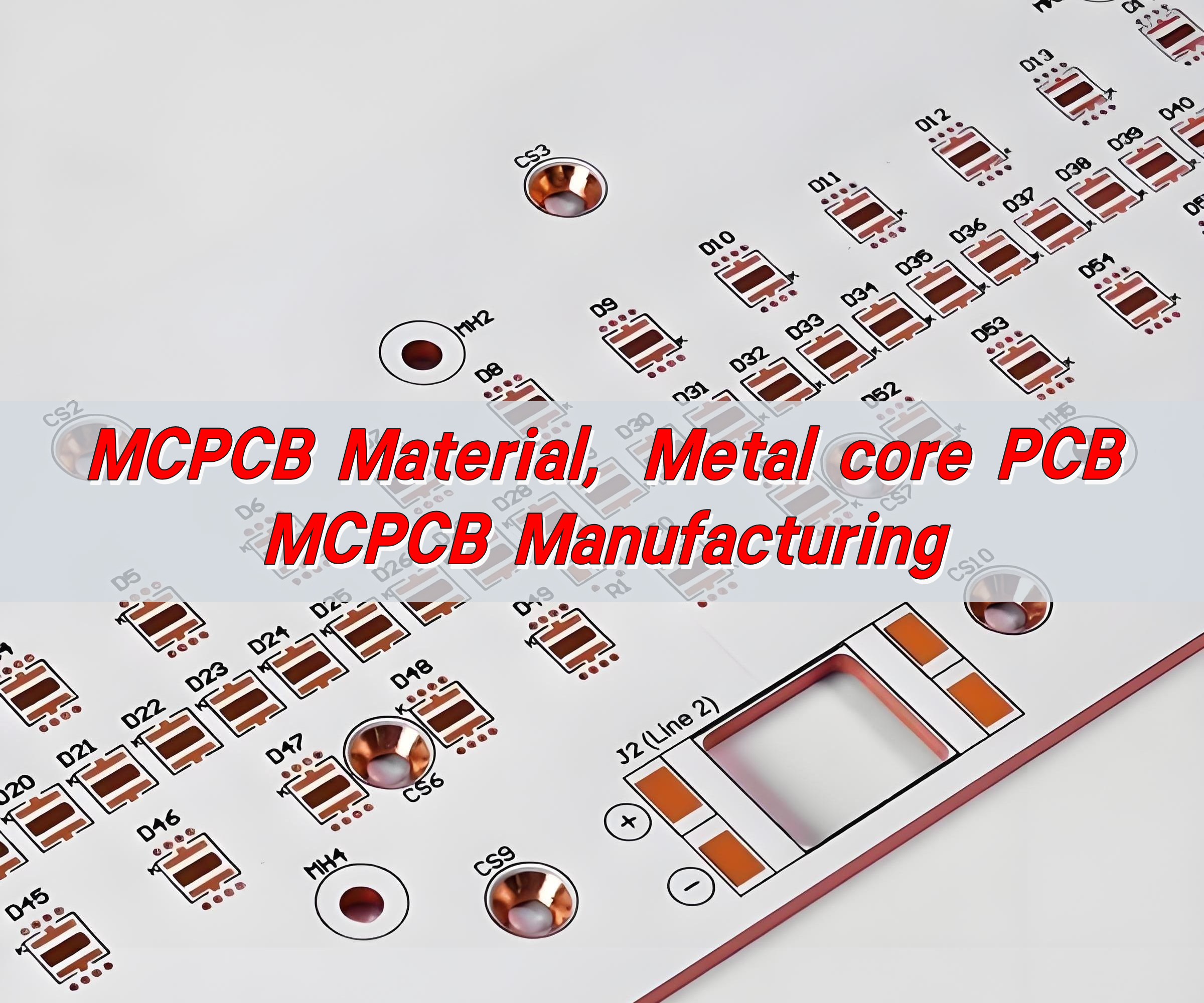
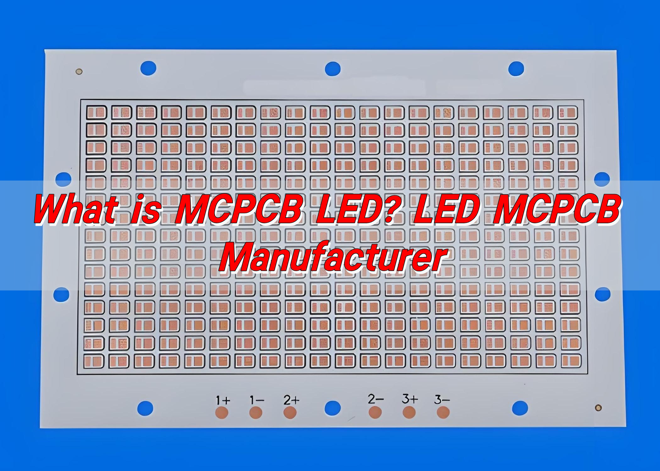
Metal Core PCBs (MCPCB) (Alternative to Aluminum)
- Why Choose It: Similar to aluminum but with different metal cores (e.g., copper) for tailored thermal needs.
- Ideal For: Applications needing a balance between cost and thermal performance.
- Pros: Flexibility in material selection (copper, iron, etc.), good for high-current designs.
- Cons: Can be heavier and more expensive than FR-4.
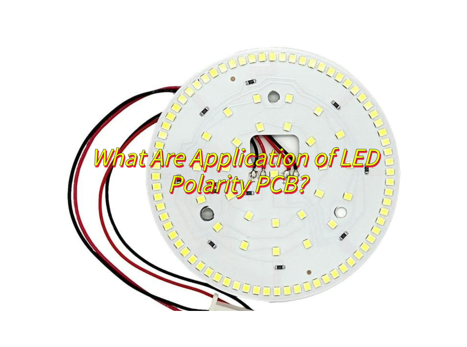
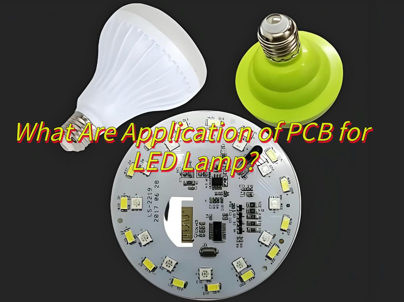
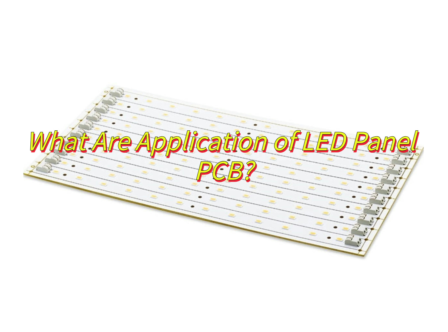
What Are Application of LED Panel PCB?
Here are application of LED Panel PCB:
- General Lighting: Used in homes, offices, and industrial spaces for energy-efficient, uniform illumination (e.g., ceiling panels, wall lights).
- Displays & Signage: Powers digital billboards, scoreboards, and video walls with vibrant visuals and 24/7 durability.
- Automotive: Provides bright, reliable lighting (headlights, taillights) and interior illumination in vehicles.
- Consumer Electronics: Enables slim, high-resolution displays in smartphones, TVs, and monitors.
- Medical: Used in surgical lights and medical equipment for precise, long-lasting illumination.
- Architectural: Offers customizable, aesthetic lighting for buildings, museums, and art installations.
- Industrial: Delivers robust lighting in factories and warehouses, improving safety and productivity.
- Specialty Lighting: Supports horticulture, aquariums, and stage lighting with tunable colors and high output.
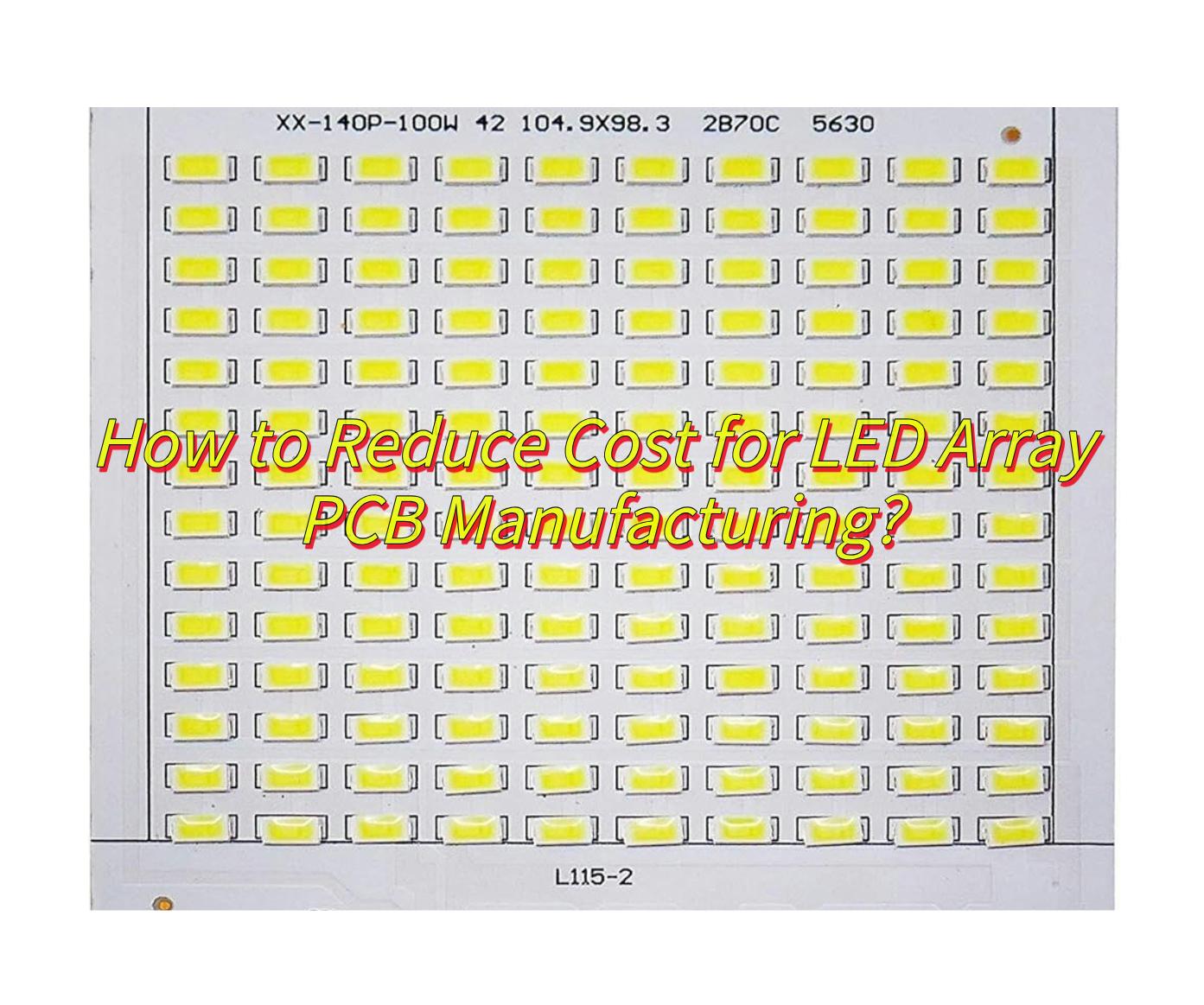
How to Balance Cost and Quality for LED Panel PCB?
Below are actionable strategies to achieve this balance and quality for LED panel PCB effectively:
1. Material Selection Optimization
- Base Material: Choose FR-4 for standard applications due to its cost-effectiveness and reliability. For high-frequency or high-power designs, consider high-TG FR-4 or metal-core PCBs (e.g., aluminum) to enhance thermal management without excessive cost.
- Copper Thickness: Prioritize for 1 oz copper for general LED lighting unless high current or thermal demands necessitate thicker layers, which increase material and processing costs.
- Surface Finishes: Use HASL (Hot Air Solder Leveling) for cost efficiency, or ENIG (Electroless Nickel Immersion Gold) for enhanced reliability in contact-heavy applications. Avoid gold plating unless critical to functionality.
2. Design Efficiency
- Layer Count: Reduce unnecessary layers by optimizing trace routing and signal integrity. A 4-layer PCB often suffices for LED lighting, avoiding the costs associated with 6- or 8-layer designs.
- Via Optimization: Minimize the use of blind/buried vias and opt for through-holes where possible. These reduce fabrication complexity and expense.
3. Manufacturing Process Control
- Fabrication Tolerance: Collaborate with manufacturers to set reasonable tolerance levels (e.g., ±0.1mm for critical dimensions) to avoid over-engineering that drives up costs.
- Testing Protocols: Implement focused testing strategies (e.g., AOI for visual defects, flying probe for connectivity) rather than 100% ICT (In-Circuit Testing) to reduce labor and equipment expenses.
- Supplier Partnerships: Work with PCB vendors offering volume discounts and flexible production scheduling. Long-term agreements can secure better pricing and priority access to advanced capabilities.
4. Thermal Management Integration
- Thermal Vias and Pads: Incorporate thermal vias and copper pours strategically to dissipate heat efficiently, reducing the need for expensive high-TG materials or additional cooling components.
- Component Placement: Position high-power LEDs and drivers to leverage natural convection paths, minimizing the reliance on active cooling solutions that add cost.
5. Cost-Driven Design Choices
- Component Standardization: Use standard LED packages (e.g., 3535, 5050) and common driver ICs to leverage economies of scale in component procurement.
- Surface Finish Trade-offs: Balance corrosion resistance and cost by selecting finishes like OSP (Organic Solderability Preservatives) for low-cost, short-lifecycle products or ENIG for longer-term reliability.
- Material Substitutions: Where feasible, replace expensive specialty materials (e.g., high-frequency laminates) with lower-cost alternatives that meet performance requirements through design compensation (e.g., wider traces for reduced loss).
6. Quality Assurance Frameworks
- DFM (Design for Manufacturability): Engage PCB manufacturers early in the design phase to incorporate their feedback on fabricability, reducing the risk of costly redesigns.
- Quality Inspection: Implement statistical process control (SPC) to monitor key quality metrics (e.g., trace width, via integrity) during production, ensuring consistency without excessive testing.
- Reliability Testing: Conduct accelerated life testing (e.g., thermal cycling, humidity resistance) on prototypes to validate design robustness before full-scale production.
7. Supply Chain and Logistics
- Localization: Source materials and PCBs from regional suppliers to minimize shipping costs and lead times, especially for time-sensitive projects.
- Inventory Management: Use JIT (Just-In-Time) inventory strategies to reduce holding costs while ensuring material availability for production.
8. Continuous Improvement
- Design Iterations: Regularly review PCB designs for efficiency gains, such as consolidating layers or reducing component count through integration (e.g., combining functions into a single IC).
- Technology Adoption: Stay updated on advanced fabrication techniques (e.g., laser direct imaging for finer traces) that may offer cost-performance trade-offs over traditional methods.
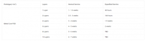
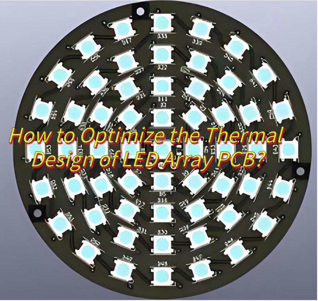
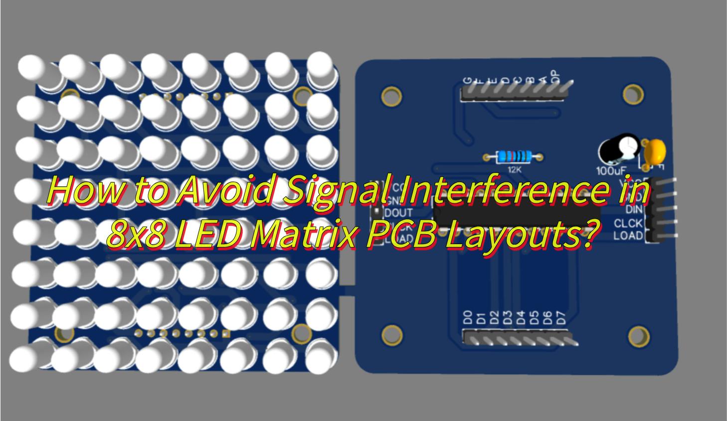
How Does PCB Layer Count Impact LED Panel Performance?
Here’s how PCB layer count impact LED panel performance:
Heat Management = Longevity
- More layers = better heat dissipation. LEDs run cooler, last longer, and avoid “burnout” spots.
- Fewer layers = risk overheating, especially in bright panels. This can shorten lifespan and cause uneven brightness.
Signal Stability = Clear Visuals
- Higher layer counts = reduced flicker, consistent color, and no ghosting. Perfect for TVs, monitors, or professional displays.
- Lower layers = potential for flickering, color shifts, or uneven lighting. Noticeable in dimmer settings or when using high brightness.
Power Efficiency = Consistent Brightness
- Dedicated power layers (in multi-layer PCBs) = even illumination across the panel. No dark corners or “hot spots.”
- Single-layer PCBs = voltage drops can lead to patchy lighting, especially in larger panels.
Smart Features = Future Prototyping
- More layers = room for dimming zones, Wi-Fi modules, or sensors. Useful if you want a “smart” panel or plan to upgrade your home system.
- Fewer layers = limited to basic on/off functionality.
Cost vs Quality
- Higher layer counts = pricier but reliable. Ideal for premium panels or long-term use.
- Lower layers = cheaper upfront but may cost more in replacements or repairs later.
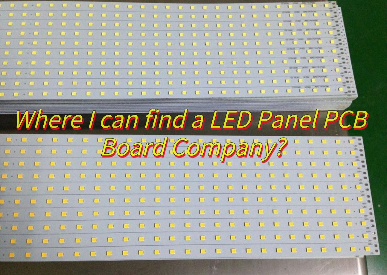
Where I can find a LED Panel PCB Board Company?
To find a reliable LED Panel PCB Board Company, follow these structured steps focusing on supplier discovery channels:
1. B2B Marketplaces
- Alibaba.com: Search “LED Panel PCB Board” to access verified suppliers offering custom PCBs, aluminum PCBs, and SMD LED integration. Filter by certifications (ISO, UL) and MOQ requirements.
- Made-in-China.com: Explore manufacturers like EBest Circuit (Best Technology) known for HDI capabilities and multi-layer PCBs tailored for LED applications.
2. Industry-Specific Directories
- PCB Pilot: A directory listing PCB manufacturers by specialty (e.g., LED lighting, automotive).
- Global Sources: Features suppliers with export capabilities, ideal for bulk orders.
3. Trade Shows & Expos
- HKTDC Hong Kong Electronics Fair: Connect with PCB manufacturers showcasing advanced LED PCB technologies.
- Electronica China: Annual event for sourcing PCBs, including those optimized for LED displays and high-power lighting.
4. Online Communities & Forums
- PCB Design Forum: Engage with engineers discussing LED PCB challenges and recommended suppliers.
- LinkedIn Groups: Join “PCB Manufacturers” or “LED Lighting Industry” to network with professionals.
5. Certification Bodies
- UL (Underwriters Laboratories): Use their database to find certified PCB manufacturers for safety compliance.
- IPC (Association Connecting Electronics Industries): Locate members specializing in LED PCB standards.
6. Referrals & Case Studies
- LED Lighting Manufacturers: Request recommendations from companies like EBest Circuit (Best Technology) for trusted PCB partners.
- Technical Blogs: Read case studies on LED PCB design (e.g., “Thermal Management in LED PCBs”) to identify suppliers mentioned in industry articles.
How to Select a Trusted LED Panel PCB Board Company?
Here’s a structured guide for selecting a trusted LED Panel PCB Board Company:
Certifications & Compliance
- Look for ISO 9001, UL, and RoHS certifications. Verify via official links or documents.
- Prefer IPC-affiliated suppliers for adherence to industry standards.
Experience & Specialization
- Choose companies with 10+ years in LED PCBs (such as EBest Circuit (Best Technology))
- Ensure expertise in thermal management and custom designs (e.g., MCPCBs, HDI).
Customization & Technical Capabilities
- Confirm ability to handle aluminum PCBs, multi-layer boards, or LED-specific features.
- Ask about in-house testing (AOI, X-Ray, Flying Probe) for defect prevention.
Quality Control
- Request sample PCBs to test functionality and compatibility.
- Prioritize suppliers with transparent quality processes (e.g., visual inspections, thermal testing).
Pricing & MOQs
- Compare quotes for standard vs. custom PCBs. Avoid hidden fees.
- Prioritize for suppliers with low MOQs (e.g., 50–100 units) if prototyping or small-scale.
Reputation & Reviews
- Check recent reviews on platforms like Alibaba, Trustpilot, or Google. Look for mentions of reliability and support.
- Seek industry recommendations (e.g., ABIS Circuits for HDI expertise).
Logistics & Support
- Ensure global shipping with tracking and clear warranties.
- Verify after-sales support (e.g., technical assistance for defects).
How to Mount LED Panel Connector on PCB to Avoid Poor Contact?
Here are some methods to mount LED panel connector on PCB to avoid poor contact:
Optimize Pad Design
- Ensure pad size matches the LED connector’s terminals to prevent misalignment or weak solder joints. Use circular or rectangular pads with proper spacing (≥0.635mm) from nearby vias to avoid thermal interference.
- Apply solder mask dams between pads and vias to isolate conductive paths and reduce solder wicking.
Control Soldering Parameters
- Maintain precise temperature profiles (e.g., 230–250°C peak) during reflow to prevent overheating, which can warp pads or degrade solder joints.
- Use solder paste with adequate viscosity and flux activity to ensure uniform coverage and avoid voids.
Ensure Proper Contact Force
- Design connectors with spring-loaded terminals to apply 0.5–1.2N of contact force on the PCB pads, ensuring stable electrical connections without damaging the LED terminals.
- Validate contact force via insertion/extraction testing (≥50 cycles) to confirm durability.
Clean Contact Surfaces
- Remove oxides, dust, or flux residues from pads and connector terminals using isopropyl alcohol or specialized cleaners before assembly.
- Apply anti-corrosion coatings (e.g., immersion gold or ENIG) to pads to maintain conductivity.
Avoid Mechanical Stress
- Use alignment guides or jigs during installation to ensure perpendicular insertion and prevent bent pins.
- Secure connectors with mounting brackets or adhesive to minimize vibration-induced loosening.
Test Conductivity Post Assembly
- Perform 100% continuity checks using milliohm meters to detect open circuits or high-resistance joints.
- Conduct environmental tests (vibration, thermal cycling) to validate long-term reliability.