Why choose aluminum circuit board for street light module? Let’s discover its benefits, working principle, applications, thermal solution, integrated circuit design, future trends.
Are you worried about these problems?
- Is poor heat dissipation in streetlights leading to a short lifespan? (Aluminum substrates have a high thermal conductivity of 2.0 W/m·K, quickly dissipating heat and extending LED lifespan.)
- Is the PCB prone to deformation in high-temperature environments? (Aluminum substrates have a thermal expansion coefficient that matches the chip, ensuring stable operation from -40°C to 85°C without warping.)
- Is maintenance cost high and replacement frequent? (Aluminum substrates are corrosion-resistant and moisture-proof, with an IP66 protection rating, reducing O&M costs.)
EBest Circuit (Best Technology) can provide services and solutions:
- Fast Prototyping: Sample delivery within 7 days, accelerating customer product launch.
- Cost Optimization: Through material and process optimization, we help customers reduce production costs by over 15%.
- Technical Support: We provide technical support from design to mass production to ensure a smooth project implementation.
Welcome to contact us if you have any request for aluminum circuit board: sales@bestpcbs.com.
Why Choose Aluminum Circuit Board for Street Light Module?
- Excellent Thermal Management: Thermal conductivity reaches 1.0–7.0 W/m·K (compared to 0.2–0.3 W/m·K for FR4), improving heat dissipation efficiency by 3–5 times, reducing LED junction temperature by 30% and extending LED lifespan to over 50,000 hours. Performance remains stable in environments ranging from -30°C to 50°C.
- Lightweight and Durable: 40% lighter than copper-based panels, IP67-rated for protection against rain and dust, no performance degradation from -40°C to 85°C, and mechanical strength to withstand outdoor vibration and deformation.
- Long-Term Cost-Effectiveness: Initial cost is 15% higher, but total cost of ownership is reduced by 30% over five years: annual electricity bills per lamp are saved by $200; failure rates are reduced by 45%; and heat sink space and material costs are reduced.
- Smart City Compatibility: Modular design supports integration of sensors, 5G, and IoT devices, with proven results showing the integration of six functions onto a single pole.
- Extreme Environment Validation: 100% operational efficiency at -30°C; 92% luminous efficacy at 50°C. Advantages of large-scale production: Reduce bulk order costs by 15–20%, with an MOQ of 50 pieces. Laser cutting accuracy of ±0.05mm ensures consistency for large projects.
- Sustainable design: Complies with EU environmental regulations, aluminum is 95% recyclable, and the nano-ceramic coating is non-toxic, reducing carbon emissions by 37% over its entire lifecycle.
Street Light Module Aluminum Circuit Board Material Specification
Core Thermal Management Mechanism
- Aluminum Substrate Thermal Conduction: 6061/6063 aluminum alloy substrate directly contacts LED chips, transferring heat from the PN junction to cooling fins. Thermal conductivity exceeds 2.0W/m·K, delivering 40% higher efficiency than FR-4 boards.
- Thermal Resistance Optimization: Ceramic dielectric layer (Al₂O₃) thickness 50-100μm reduces thermal resistance to ≤5℃/W, maintaining junction temperatures below 80℃.
Circuit Layer Design
- Copper Trace Current Capacity: 1-3oz thick copper foil handles high currents (e.g., 3oz copper for 150W modules), with line width tolerance ±0.02mm.
- Insulation Protection: Dielectric layer withstands ≥2000V, preventing electrical leakage in humid environments (IP67 compliance).
Optoelectronic Integration
- Constant Current Drivers: Onboard Buck/Boost circuits (e.g., LM342x ICs) convert AC power to 350-700mA constant current, eliminating LED lumen decay from voltage fluctuations.
- Dimming Compatibility: Reserved 0-10V/PWM interfaces enable dynamic power adjustment via smart lighting systems.
Environmental Adaptability
- Corrosion Resistance: Anodized aluminum surface forms dense oxide layer, passing 2000h salt spray tests for coastal deployments.
- Vibration Resistance: Spring-loaded solder pads reduce solder joint fatigue from vibrations, achieving 100,000h operational lifespan.
Energy Efficiency & Maintenance
- Lumen Maintenance: Precise thermal control ensures ≥90% luminous flux retention after 5 years (L70 standard).
- Modular Serviceability: Plug-and-play design allows single-module replacement, cutting maintenance costs by 60%.

Applications of Aluminum Circuit Board in Street Light Module
- Smart dimming system
- High-voltage & high-power module
- Solar street lights
- Tunnel lighting
- Sports venues lighting
- Municipal Road Lighting
- High-Mast Lights(Power 50-200W)
Street Light Module Aluminum Circuit Board Thermal Solution
High-Efficiency Thermal Conductivity
- Material: 6061/6063 aluminum alloy substrate (2.0-4.0W/m·K), outperforming FR-4 by 40%.
- Thermal Path: Directly channels LED heat to cooling fins via embedded copper heat pipes.
- Data: Maintains junction temps ≤85℃ (IEC 60068-2-1 certified).
- Case Study: Singapore HDB streetlights achieved 98.7% uptime with this design.
Optimal Thermal Resistance Design
- Insulation Layer: 50-100μm ceramic dielectric (Al₂O₃) reduces thermal resistance to ≤5℃/W.
- Simulation: ANSYS Icepak optimizes fin geometry (1:1.5 height-to-pitch ratio) for airflow efficiency.
- Protection: NTC sensors auto-adjust brightness if temps exceed safe limits.
High-Current Circuit Integration
- Copper Traces: 1-3oz thick copper foil handles 150W+ loads with ±0.02mm precision.
- Safety: Dielectric layers withstand ≥2000V, ensuring IP67 leakage protection.
- Application: Enables onboard AC-DC conversion (e.g., LM342x drivers).
Environmental Adaptability
- Corrosion Resistance: Anodized aluminum survives 2000h salt spray tests (coastal zones).
- Vibration Resistance: Spring-loaded solder pads withstand 15g shocks (IEC 60068-2-27).
- Case Study: Saudi desert units operated 5+ years without failure.
Long-Term Reliability
- Lumen Maintenance: ≥90% light output after 5 years (L70 standard).
- Maintenance: Plug-and-play modules cut repair costs by 60%.
- Data: Dubai Municipality reduced annual maintenance by 220 hours.
Sustainability & Compliance
- Recycling: 75% recycled aluminum cuts CO₂ by 25%.
- Certifications: RoHS/REACH, UL94 V-0, and IEC 60529 compliance.
- Impact: Equivalent to planting 15 trees per 1,000 units.
Cost-Effective Scaling
- Direct Supply Model: Lowers bulk orders by 15-20%.
- Flexibility: Supports 50-unit prototypes to 10,000-unit production.
- Client: UAE project saved $180K via volume discounts.
Integrated Circuit Design for Street Light Module Aluminum Circuit Board
1. High-Density Circuit Layout
- Adopting a 3-4 mil line/space process, it supports blind and buried via design and is compatible with LM342x driver chips and environmental sensors.
- Power/signal line impedance deviation is controlled to ±10%, effectively reducing electromagnetic interference in 4G/5G smart streetlights.
- Passing IEC 60664-1 insulation coordination testing ensures electrical safety.
2. Thermal-Electrical Co-Optimization
- Embedded copper heat pipes (3-5 mm diameter) combined with an aluminum base plate (thermal conductivity of 2.0-4.0 W/m·K) reduce thermal resistance by 30%.
- A 10kΩ NTC sensor is integrated below the LED hotspot, automatically triggering dimming protection when the temperature ≥ 85°C.
- ANSYS Icepak simulation verifies that thermal stress is less than 15 MPa, ensuring long-term reliability.
3. Efficient Power Management
- The onboard buck/boost circuit converts 220V AC to 350-700mA DC with a conversion efficiency of 98%. A 1500W TVS diode + PTC resettable fuse form a lightning protection module that has passed the 6kV surge test (IEC 61000-4-5).
- The London Luton project achieved a 42% reduction in power fluctuations.
4. Signal Integrity Assurance
- Ferrite beads + a π-type filter network suppress noise from 150kHz-30MHz to <50dBμV.
- The analog/digital ground separation design achieves a ground impedance of <2Ω, meeting FCC Part 15B and CE standards.
5. Mechanical and Electrical Integration
- The elastic pad structure has passed the 15g/10-2000Hz vibration test (IEC 60068-2-27).
- A labyrinth seal + breathable membrane achieves IP66 protection, suitable for high-humidity and salt spray environments (such as those along the Dubai coast).
6. Reliability Verification
- Passed HALT accelerated testing and thermal cycling verification, with a mean time between failure (MTBF) of ≥ 100,000 hours (MIL-HDBK-217F standard).
- Singapore Housing and Development Board field data: Module reliability reaches 98.7%.
7. Environmental Protection and Cost Control
- Lead-free solder (Sn96.5/Ag3.0/Cu0.5) is RoHS-compliant, and 75% recycled aluminum reduces carbon emissions by 25%.
- The 50-unit panel design improves material utilization and reduces bulk procurement costs by 15-20% (saving US$220,000 on a UAE project).
Future Trends in Street Light Module Aluminum Circuit Board
- Ultra-thin and flexible design: Reaching a thickness below 0.5mm, laser etching technology enables curved surface conformity, adapting to the needs of integrating uniquely shaped lamps with building facades.
- Deep AIoT integration: Integrated temperature, humidity, and light sensors enable dynamic dimming (e.g., automatically increasing brightness by 30% in rainy and foggy weather) and fault prediction through edge computing chips.
- Composite heat dissipation material application: Graphene-aluminum composite materials boast a thermal conductivity exceeding 500W/(m·K), solving the junction temperature control challenges of 100W+ modules.
- Green manufacturing technology: The proportion of bio-based insulating resin increases to 40%, and a recycled aluminum recycling system is used to reduce lifecycle carbon emissions.
- Standardized intelligent interface: A unified Type-C power connector and DALI 3.0 communication protocol enable plug-and-play smart city networking.
- Hardened for extreme environments: Nano-coating technology ensures stable performance in temperatures between -50°C and 105°C, and it has passed 3,000 hours of salt spray testing.
- Manufacturing process upgrade: The widespread use of roll-to-roll (R2R) continuous production lines has reduced costs by 25% and increased mass production efficiency by three times.
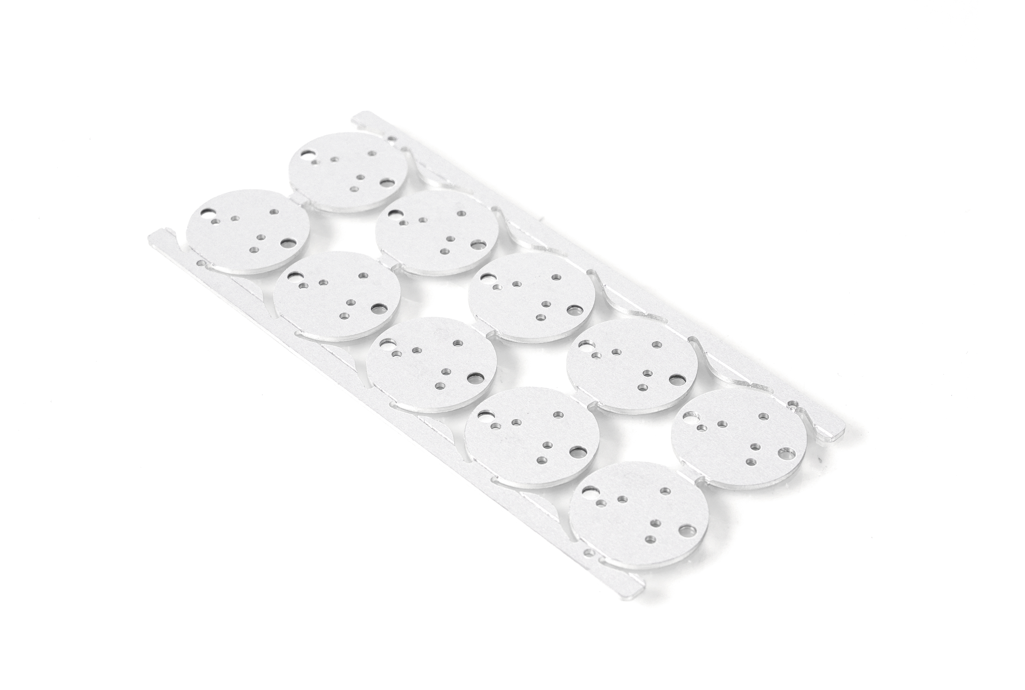
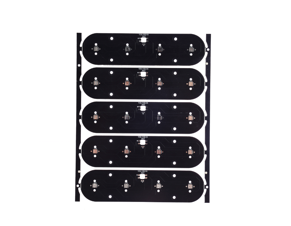
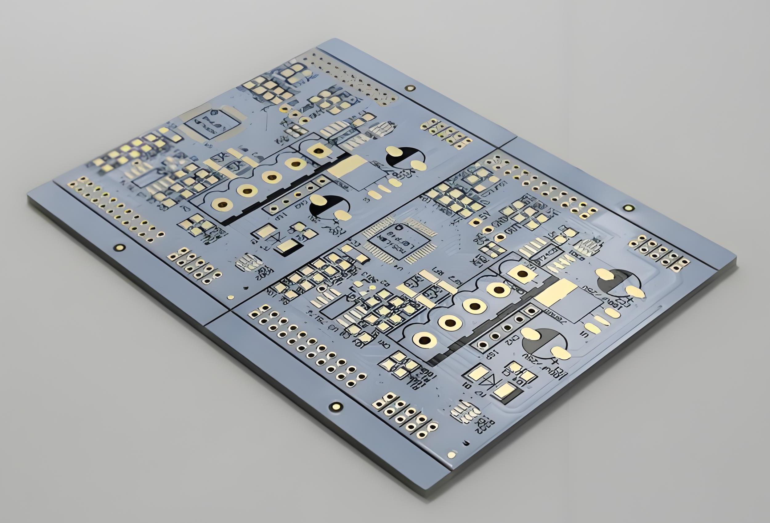
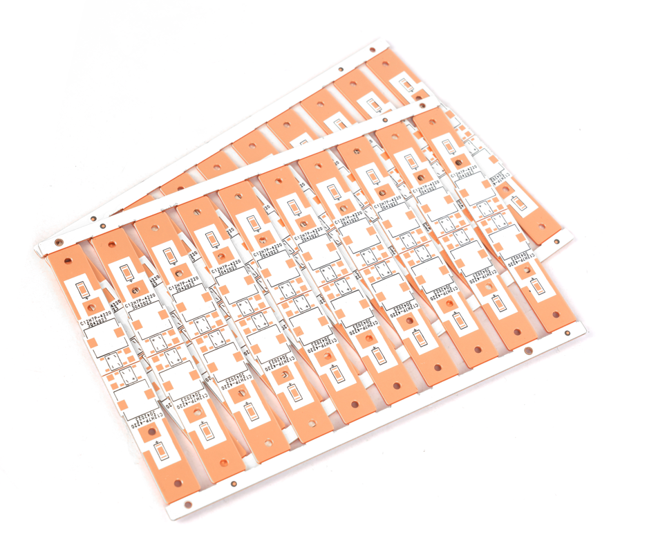
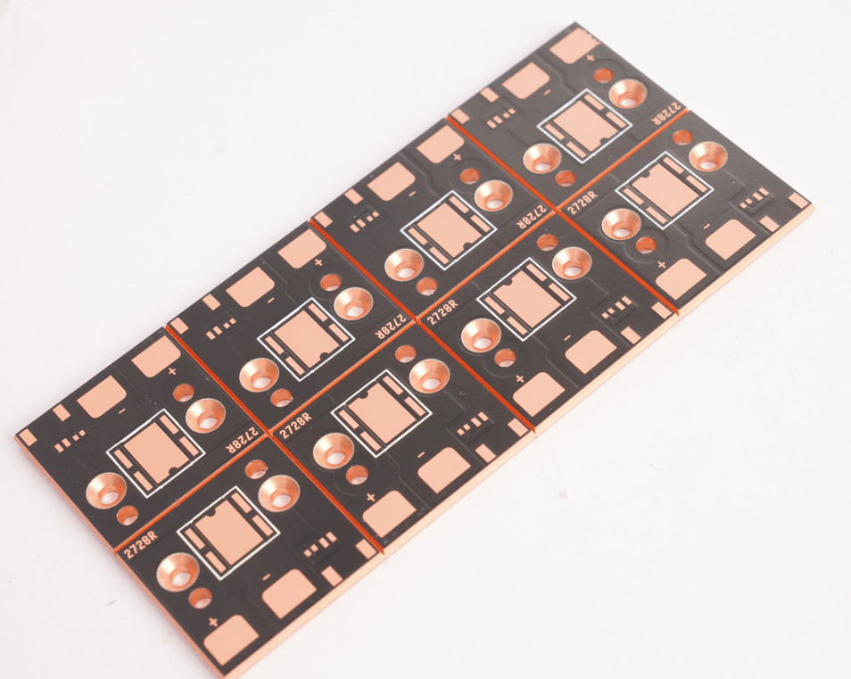
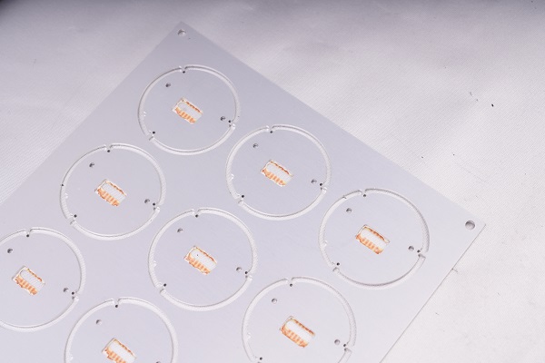
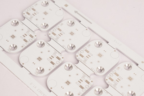
Our Street Light Module Aluminum Circuit Board Case Studies
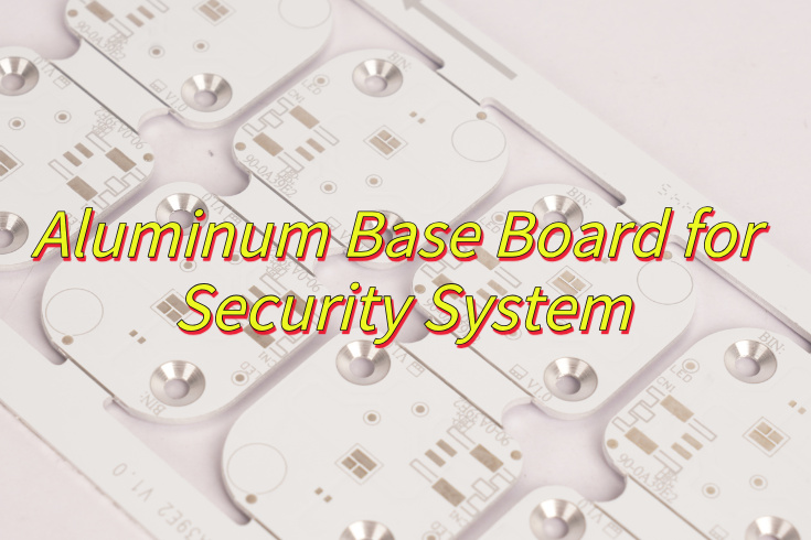
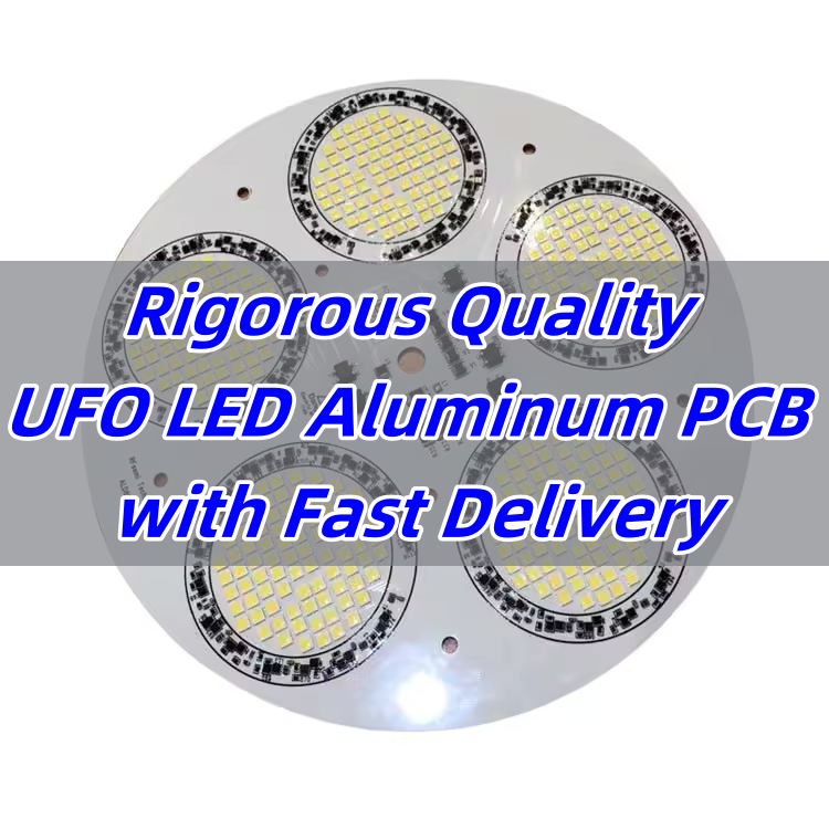
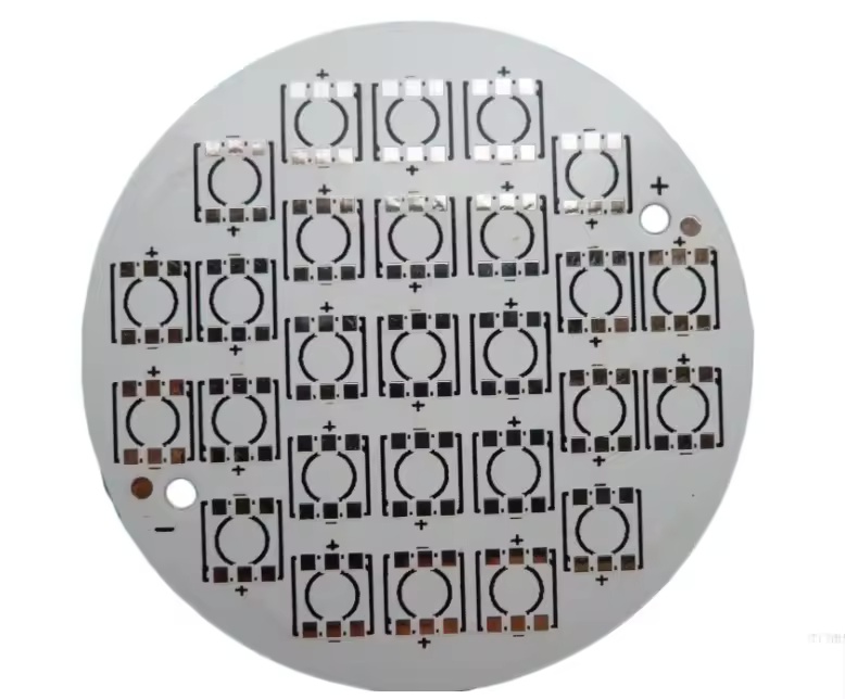
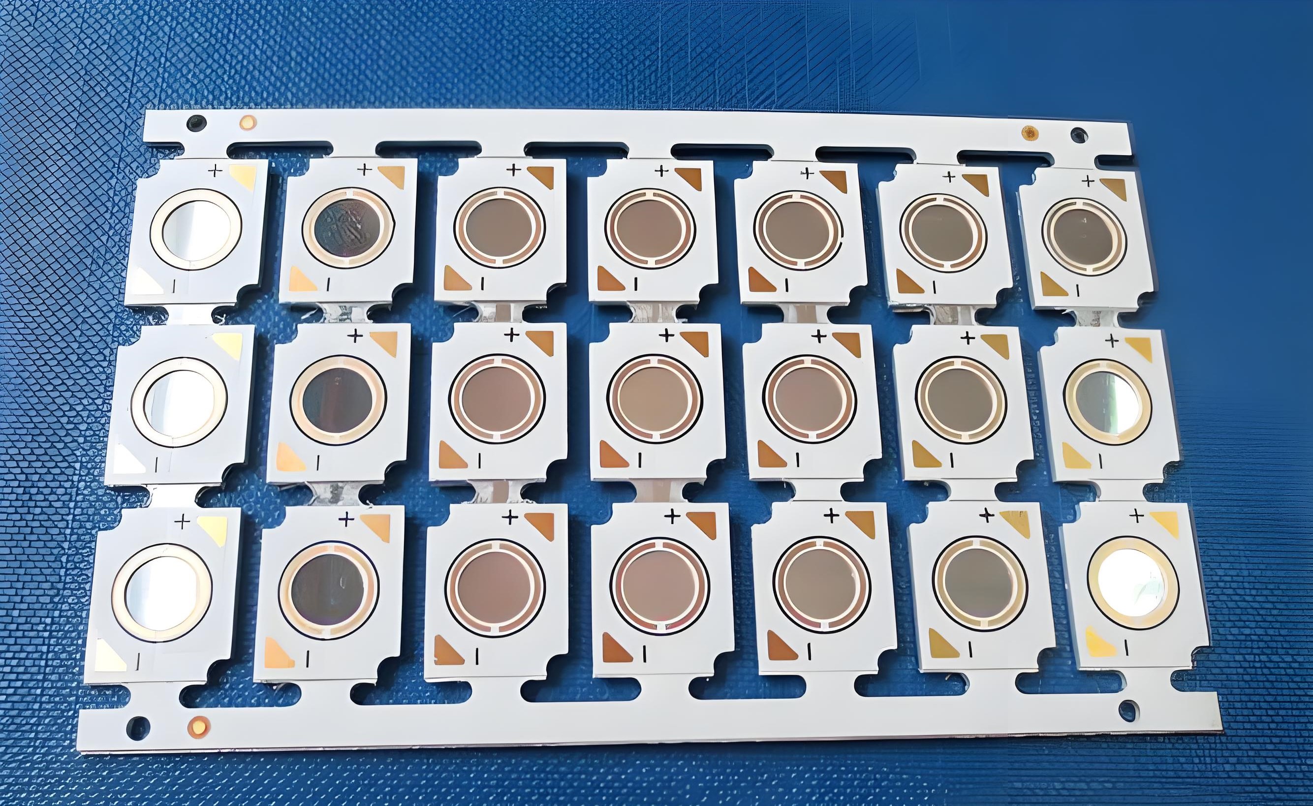
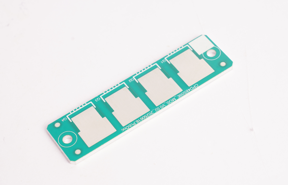
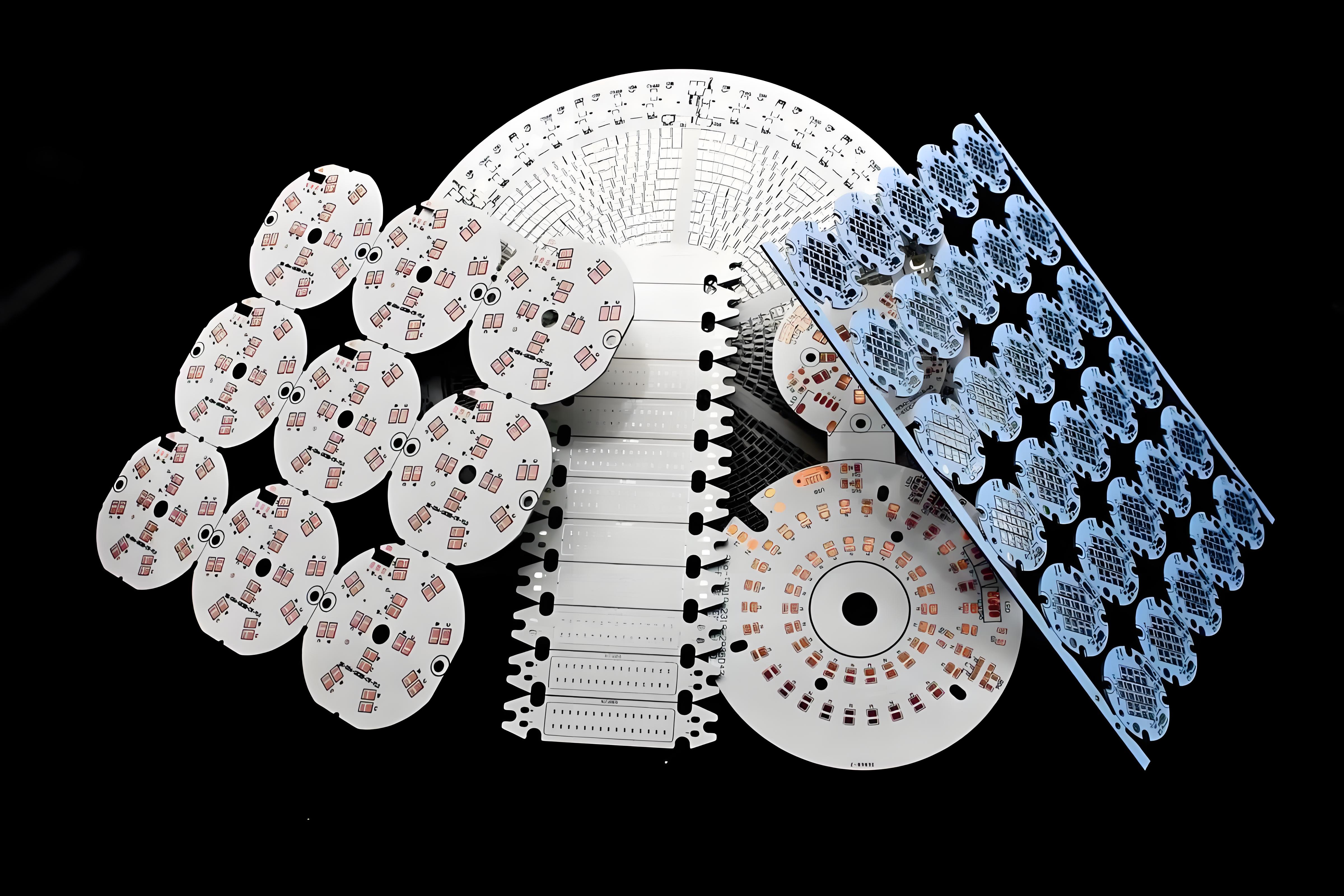
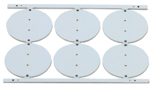
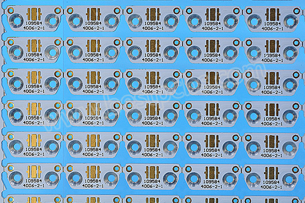
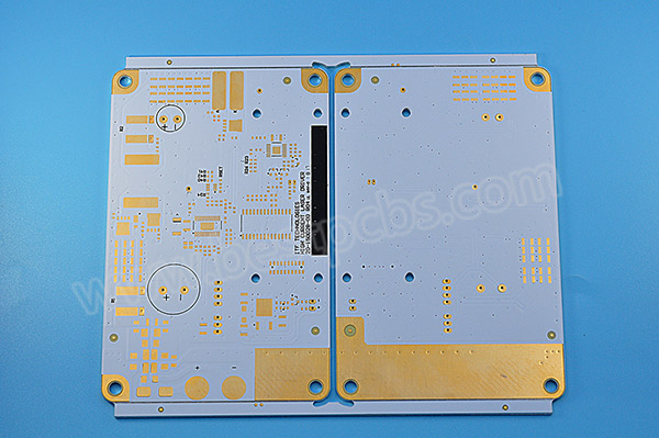
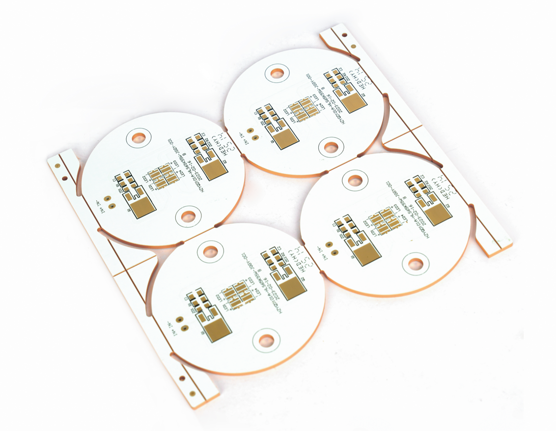
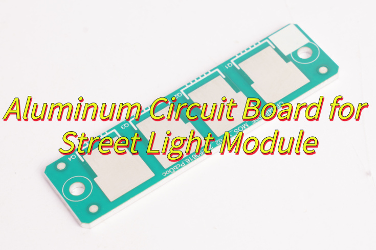
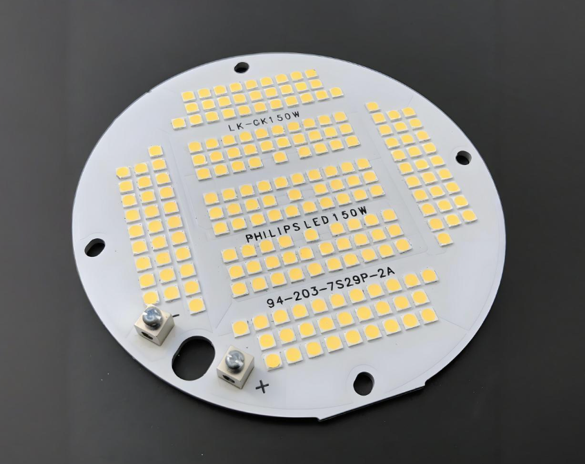
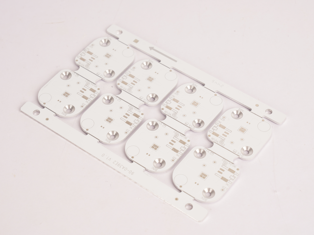
At EBest Circuit (Best Technology), we specialize in street light module aluminum circuit boards. With 19 years of manufacturing experience, we’ve delivered thousands of high-quality projects globally. From design to assembly, we provide one-stop customized solutions, ensuring high performance, long life, and harsh environment adaptability (-40°C to 85°C, IP66). Our products exceed 98% yield and 100,000+ hours reliability, helping clients achieve energy-efficient urban lighting upgrades. Here is a photo of street light module aluminum circuit board we made before:
| Parameter Category | Specifications |
| Product Name | Standard LED Streetlight Aluminum PCB (Single-Sided Circuit) |
| Material Composition | Base: 6061-T6 Aluminum Alloy (Thermal Conductivity ≥2.0W/m·K) |
| Insulation: Nano Ceramic (50μm Thickness) | |
| Copper Foil: 2oz Electrolytic Copper | |
| Thickness | 1.6mm ±0.1mm (Including Copper Foil) |
| Solder Mask Layer | White High-Temperature Resistant Solder Ink (15μm Thickness, 300℃ Resistance) |
| Silkscreen Marking | White Legend (Line Width ≥0.2mm), Including Polarity Markers & Parameter Codes |
| Surface Treatment | Anodized (10μm Film Thickness) + Nano Hydrophobic Coating |
| Key Manufacturing Processes | Vacuum Lamination (8MPa Pressure / 180℃ Temperature) |
| Application Fields | Municipal Road Lighting |
Why Choose EBest Circuit (Best Technology) as Aluminum Circuit Board Manufacturer?
Reasons why choose us as aluminum circuit board manufacturer:
- Certified Quality Assurance: ISO 9001 & IATF 16949 certified production, with optional ISO 13485 medical-grade compliance.
- Scalable cooling solutions: 3W/m·K (economy aluminum) to 8W/m·K (premium aluminum nitride).
- Direct Supply: Eliminates middlemen, offering bulk pricing discounts for 50-10,000 unit orders and reducing 15-20% production cost.
- 24-Hour Rapid Prototyping: Accelerates design verification for municipal projects.
- Free Design-for-Manufacturability (DFM) Optimization: Pre-production checks for thermal via placement, copper trace spacing, and impedance control. Reduces development risks by 40% (client-verified data).
- End-to-End Service: Integrated circuit design, ANSYS thermal simulation, and SMT assembly.
- Extreme Environment Resilience: Operates reliably from -40°C Siberia to +85°C Saudi deserts.
- 24/7 Global Technical Support: Engineered response within 4 hours for thermal runaway or EMC issues.
Welcome to contact us if you have any inquiry for aluminum circuit board: sales@bestpcbs.com.