Looking for PCB Design and fabrication solutions? This guide explores design flaw detection, signal integrity solutions, cost-effective fabrication, and integrated service selection for efficient PCB development.
EBest Circuit (Best Technology) solves these challenges with our reliable one-stop PCB design and fabrication services. We offer free DFM analysis to eliminate 90% of manufacturing issues before production begins, saving you time and money on reworks. For urgent needs, our 24-hour rapid prototyping service delivers with 98% on-time accuracy—no more missed deadlines. Whether you need 1-piece prototypes or high-volume orders, we handle everything from complex HDI and high-speed boards to RF designs, backed by 18+ years of specialized experience. Every PCB undergoes 100% inspection using advanced AOI and flying probe testing, ensuring defect rates below 500ppm. With transparent pricing (typically 15-20% more cost-effective than competitors) and no hidden fees, we make budgeting predictable. Over 1,200 global clients trust us to combine precision engineering with fast turnaround. Submit your design today for a risk-free quote within 24 hours and experience stress-free PCB manufacturing: sales@bestpcbs.com.
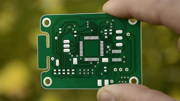
What Is PCB Design?
PCB design is the process of planning and arranging electronic circuits on a board to create functional connections. Engineers begin by drafting a schematic to map out how components should link together, then carefully position each part and draw conductive pathways between them. This stage requires attention to both electrical behavior, like maintaining clean signals and stable power flow, and physical limitations such as board dimensions and layer arrangements. Designers follow specific manufacturing guidelines for trace widths, hole placements, and material choices to guarantee the board can be reliably produced. More complex designs might need specialized techniques for handling fast signals, matching impedance, or managing heat buildup. A well-executed PCB design transforms circuit ideas into practical, manufacturable boards that power devices ranging from everyday gadgets to advanced industrial equipment. For streamlined development, services combining design and fabrication help align creative choices with production realities from the start.
How to Catch PCB Design Flaws Early to Prevent Project Halts?
- Leverage Design Rule Checks (DRC): Run automated DRC tools at every major design milestone. Configure rules to match fabrication capabilities (e.g., minimum trace width, clearance). Address violations immediately to avoid compounding errors.
- Simulate Before Prototyping: Use signal integrity (SI) and power integrity (PI) simulations for high-speed designs. Identify issues like crosstalk or voltage drops early, reducing costly re-spins.
- Cross-Functional Reviews: Organize collaborative reviews with layout engineers, firmware developers, and manufacturers. Fresh perspectives often reveal overlooked gaps (e.g., thermal management, testability).
- Test Point Accessibility: Ensure test points are logically placed and unobstructed. This simplifies debugging and avoids post-production surprises.
- Component Footprint Validation: Double-check footprints against datasheets before finalizing the layout. Mismatched pads or 3D model collisions can halt assembly.
- Thermal Analysis: Model heat dissipation for power components. Poor thermal design leads to field failures, especially in compact layouts.
- DFM/DFA Audits: Partner with fabricators to review design-for-manufacturability (DFM) and assembly (DFA) guidelines. Adjustments like solder mask spacing can prevent yield losses.
- Early Prototyping: Order small-batch prototypes to validate physical performance. Functional testing at this stage exposes flaws masked in simulations.
- Version Control & Documentation: Maintain clear revision logs and annotate design changes. Confusion over file versions often causes delays.
- Supply Chain Alignment: Verify component availability and lifecycle status during design. Last-minute substitutions due to obsolete parts derail timelines.
How to Prevent Signal Integrity and Crosstalk Issues in High-Speed PCB Design?
Methods about how to prevent signal integrity and crosstalk issues in high-speed PCB design:
- Prioritize Controlled Impedance Traces: Maintain consistent impedance across high-speed signal paths by defining precise trace widths, dielectric thicknesses, and copper weights. Use impedance calculation tools during layout planning to align with your PCB stack-up design. Consistent impedance reduces reflections and ringing, which are common causes of signal degradation.
- Optimize Trace Routing and Spacing: Route high-speed signals on dedicated layers with continuous ground planes beneath them to minimize electromagnetic interference (EMI).Increase the spacing between aggressive (aggressor) and victim traces to reduce crosstalk. A rule of thumb is to maintain a gap of at least three times the trace width between parallel runs.
- Implement Differential Pair Routing: Use differential pairs for high-speed differential signals (e.g., USB, HDMI, PCIe) to enhance noise immunity. Route pairs symmetrically with matched lengths and equal spacing to preserve signal balance. Avoid inserting vias or stubs into differential pairs, as these disrupt impedance continuity.
- Limit Parallel Trace Lengths: Minimize the length of parallel trace segments between unrelated signals. Crosstalk severity increases with both parallel length and signal rise time. If parallel routing is unavoidable, use guard traces (connected to ground) between aggressors and victims to absorb unwanted coupling.
- Choose Low-Loss Dielectric Materials: Select PCB laminates with low dielectric constants (Dk) and low dissipation factors (Df) to reduce signal attenuation and phase distortion at high frequencies. Materials like FR4-grade laminates with optimized resin systems strike a balance between cost and performance for mid-range speeds.
- Incorporate Proper Termination Strategies: Apply series or parallel termination resistors at the source or receiver ends of high-speed traces to match impedance and dampen reflections. For multi-drop buses, use AC-coupled termination to accommodate varying voltage levels without signal distortion.
- Validate Designs with Pre-Layout Simulations: Perform SI simulations early in the design cycle to predict issues like overshoot, undershoot, and ringing. Tools like IBIS models or SPICE simulators help evaluate driver/receiver behavior and identify required adjustments before finalizing the layout.
- Use Post-Layout Extraction and Analysis: After routing, extract the PCB’s parasitic elements (e.g., capacitance, inductance) and re-simulate to validate performance under real-world conditions. Address discrepancies by tweaking trace geometry, termination, or topology.
- Isolate Noisy and Sensitive Circuits: Separate high-speed digital circuits from analog or low-noise components (e.g., RF modules, sensors) using ground planes or isolation trenches. This reduces EMI and prevents noise coupling into vulnerable sections.
- Collaborate with Manufacturers for DFM Input: Share your design with your PCB fabricator early to leverage their expertise in high-speed materials and stack-up configurations. They can advise on feasible trace/space tolerances, via structures, and impedance control methods aligned with their production capabilities.
- Test Prototypes with Advanced Validation Tools: During prototyping, use time-domain reflectometry (TDR) or bit-error-rate testing (BERT) to validate signal quality. These tests uncover hidden SI issues like impedance discontinuities or jitter that simulations might miss.
- Document and Enforce Design Guidelines: Create a checklist of SI/crosstalk rules tailored to your project’s speed and complexity. Train your team to follow these guidelines consistently, reducing variability and rework.
How to Handle Frequent Design Changes without Increasing Project Time and Expenses?
Here are ways about how to handle frequent design changes without increasing project time and expenses:
- Design for Consistent Impedance: Calculate and maintain precise impedance values across all high-speed traces. Use impedance calculation tools during layout planning to define trace widths, dielectric thicknesses, and copper weights that align with your PCB stack-up. Consistent impedance minimizes reflections and ringing, which are primary causes of signal degradation.
- Route Traces Strategically: Avoid parallel routing of unrelated signals whenever possible. If parallel traces are unavoidable, limit their length and increase the spacing between them (ideally three times the trace width). Additionally, incorporate guard traces connected to ground between potential aggressor and victim nets to absorb unwanted noise.
- Adopt Differential Pair Routing: For differential signals (e.g., USB 3.0, HDMI, Ethernet), route pairs symmetrically with matched lengths and fixed spacing. This approach enhances noise immunity and reduces susceptibility to common-mode interference. Avoid vias or stubs in differential pairs to preserve signal integrity.
- Choose Low-Loss Dielectric Materials: Select PCB laminates with low dielectric constants (Dk) and dissipation factors (Df) to minimize signal loss at high frequencies. Materials like FR4-grade laminates with optimized resin systems offer a balance between cost and performance for mid-range speed requirements.
- Implement Proper Termination: Apply series or parallel termination resistors at the source or receiver ends of high-speed traces to match impedance and dampen reflections. For multi-drop buses, consider AC-coupled termination to accommodate varying voltage levels without distortion.
- Simulate Early and Iterate: Perform pre-layout SI simulations to predict issues like overshoot, undershoot, and ringing. After routing, extract parasitic elements and re-simulate to validate performance under real-world conditions. Address discrepancies by adjusting trace geometry, termination, or topology.
- Isolate Sensitive Circuits: Separate high-speed digital circuits from analog or low-noise components (e.g., RF modules, sensors) using ground planes or isolation trenches. This reduces electromagnetic interference (EMI) and prevents noise coupling into vulnerable sections.
- Collaborate with Your Fabricator: Share your design with your PCB manufacturer early to align with their production capabilities. They can advise on feasible trace/space tolerances, via structures, and impedance control methods, avoiding costly rework later.
- Validate with Advanced Testing: During prototyping, use tools like time-domain reflectometry (TDR) or bit-error-rate testing (BERT) to uncover hidden SI issues. These tests provide critical insights into impedance discontinuities or jitter that simulations might miss.
- Document and Enforce Design Rules: Create a checklist of SI/crosstalk guidelines tailored to your project’s needs. Train your team to follow these rules consistently, reducing variability and ensuring high-quality outcomes.
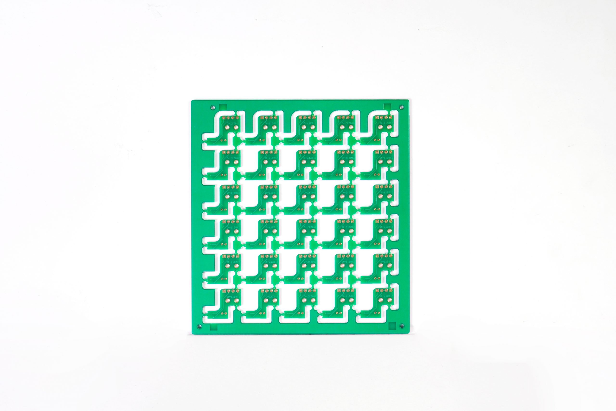
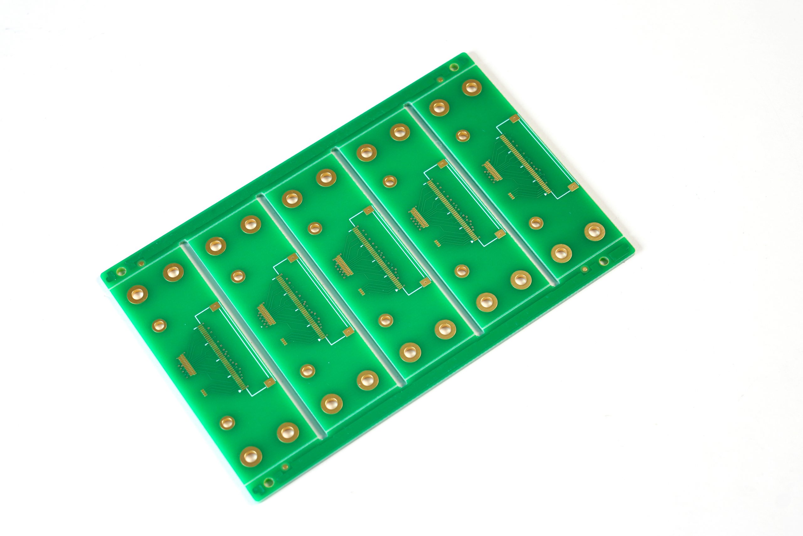
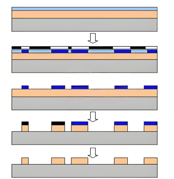
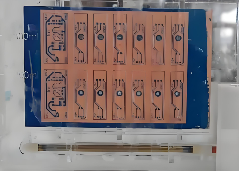
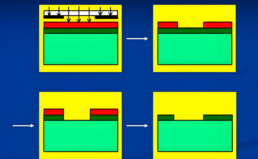
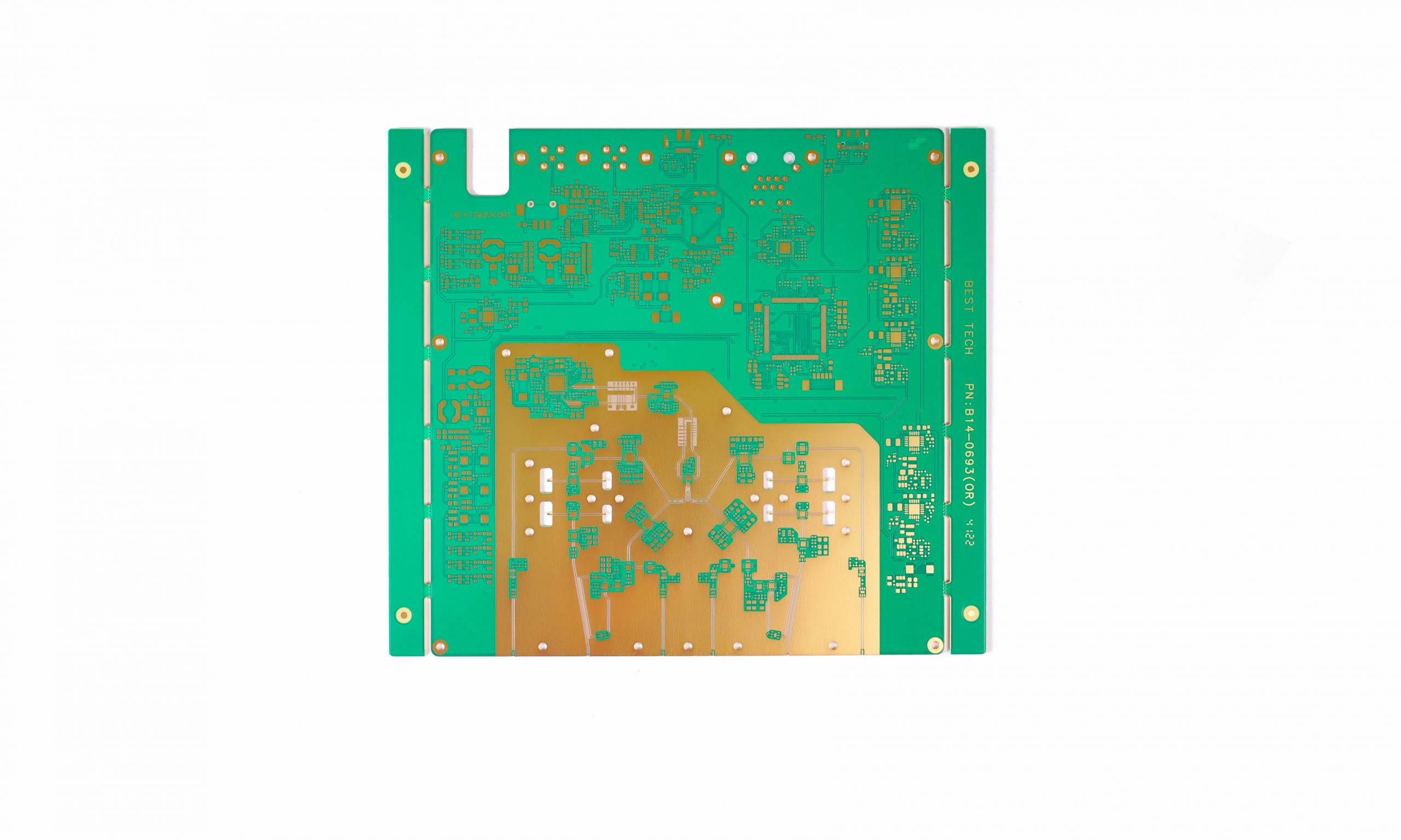
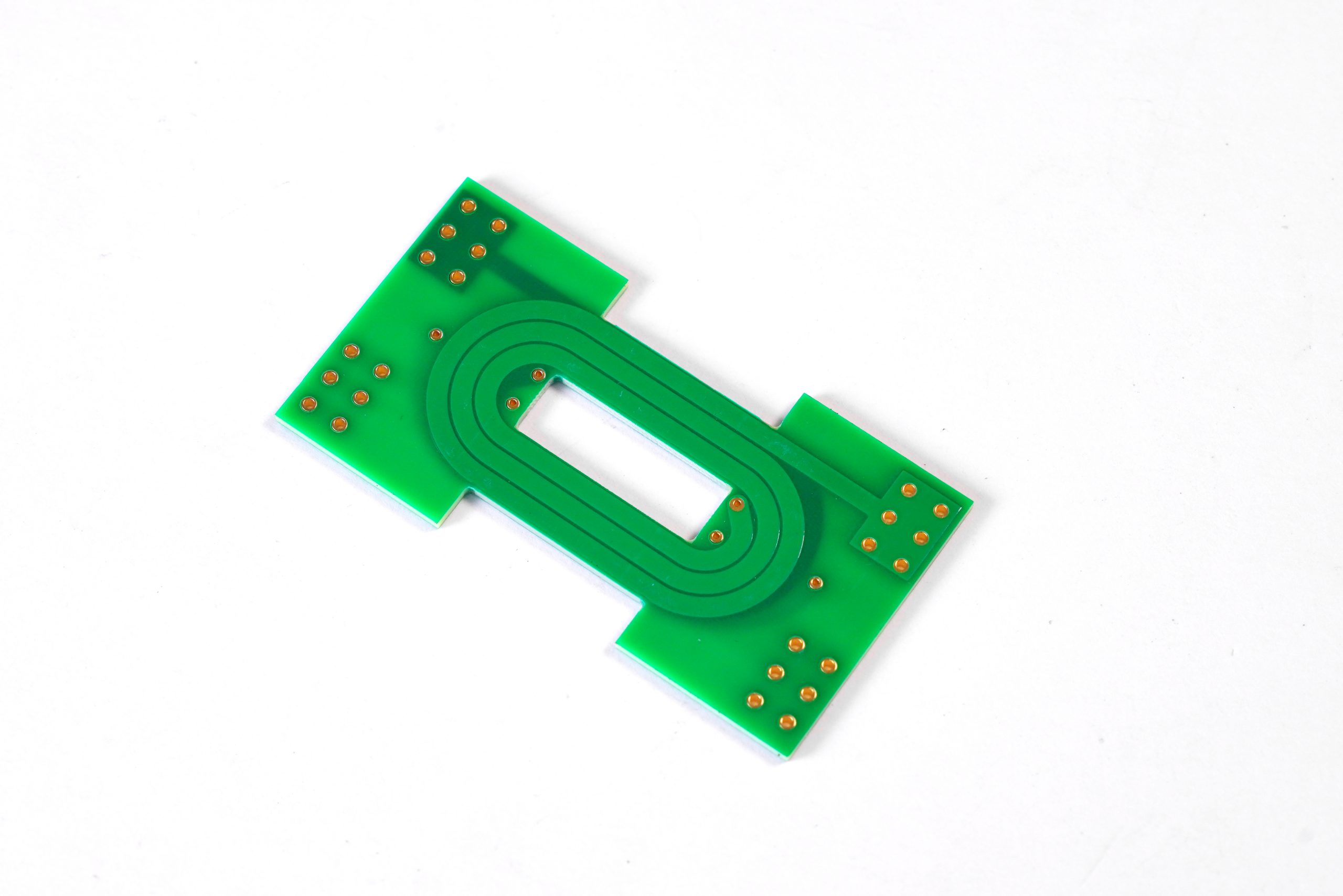
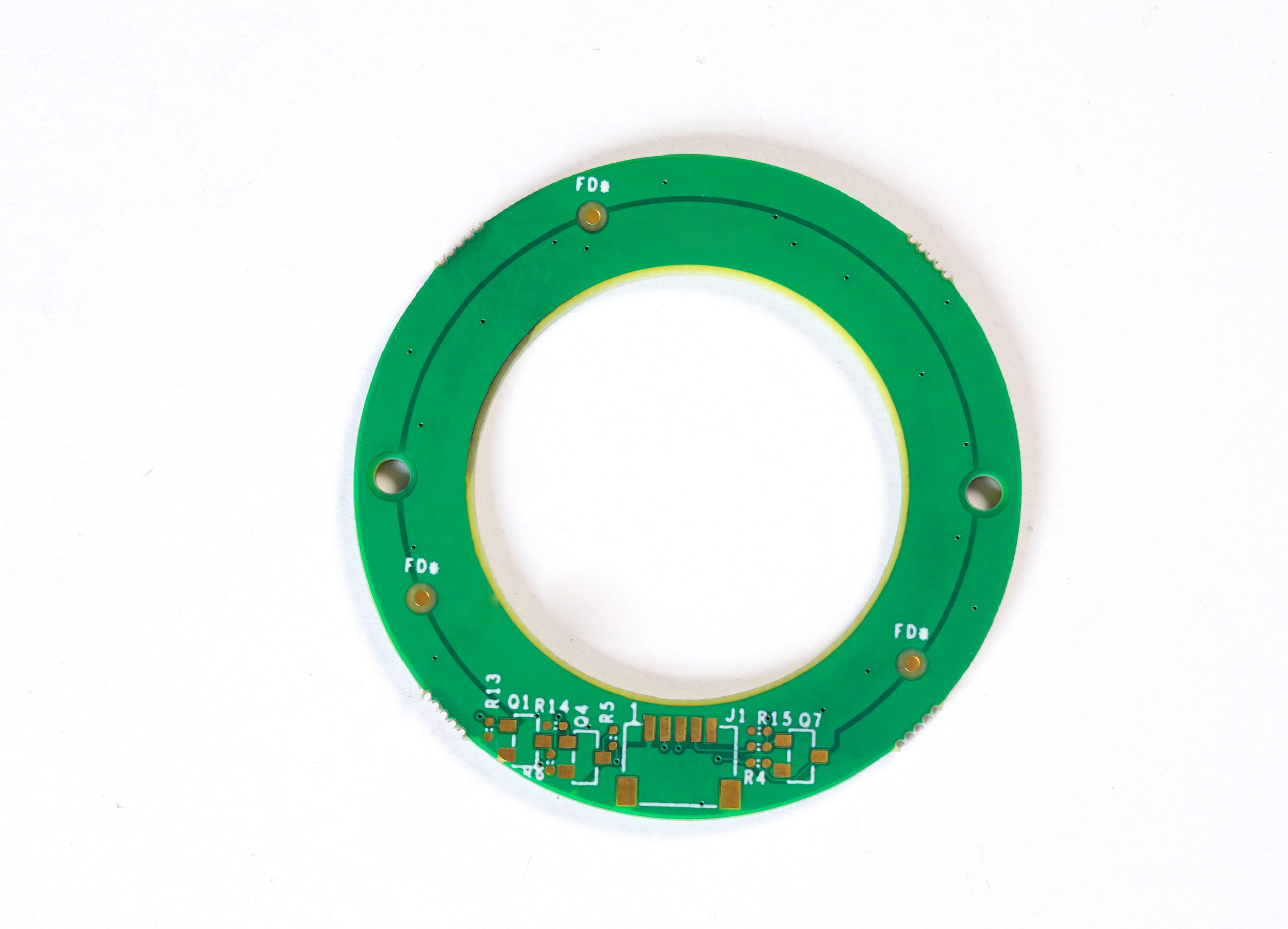
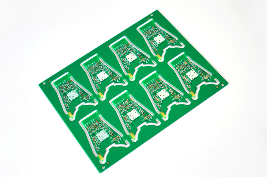
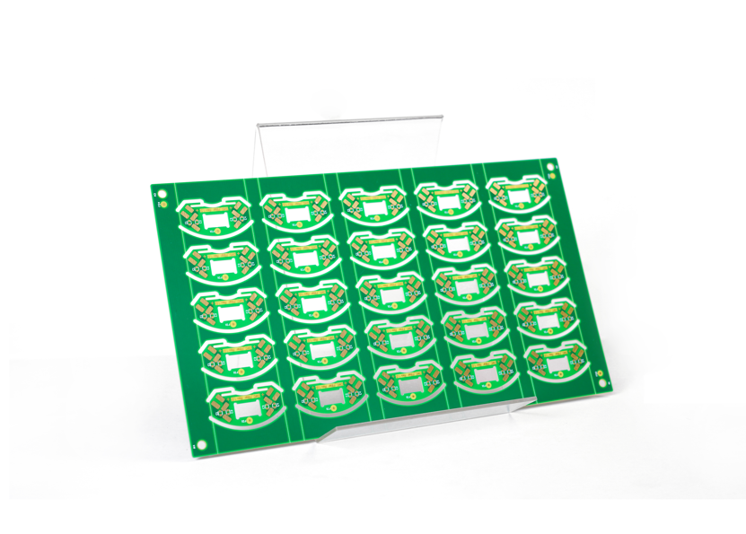
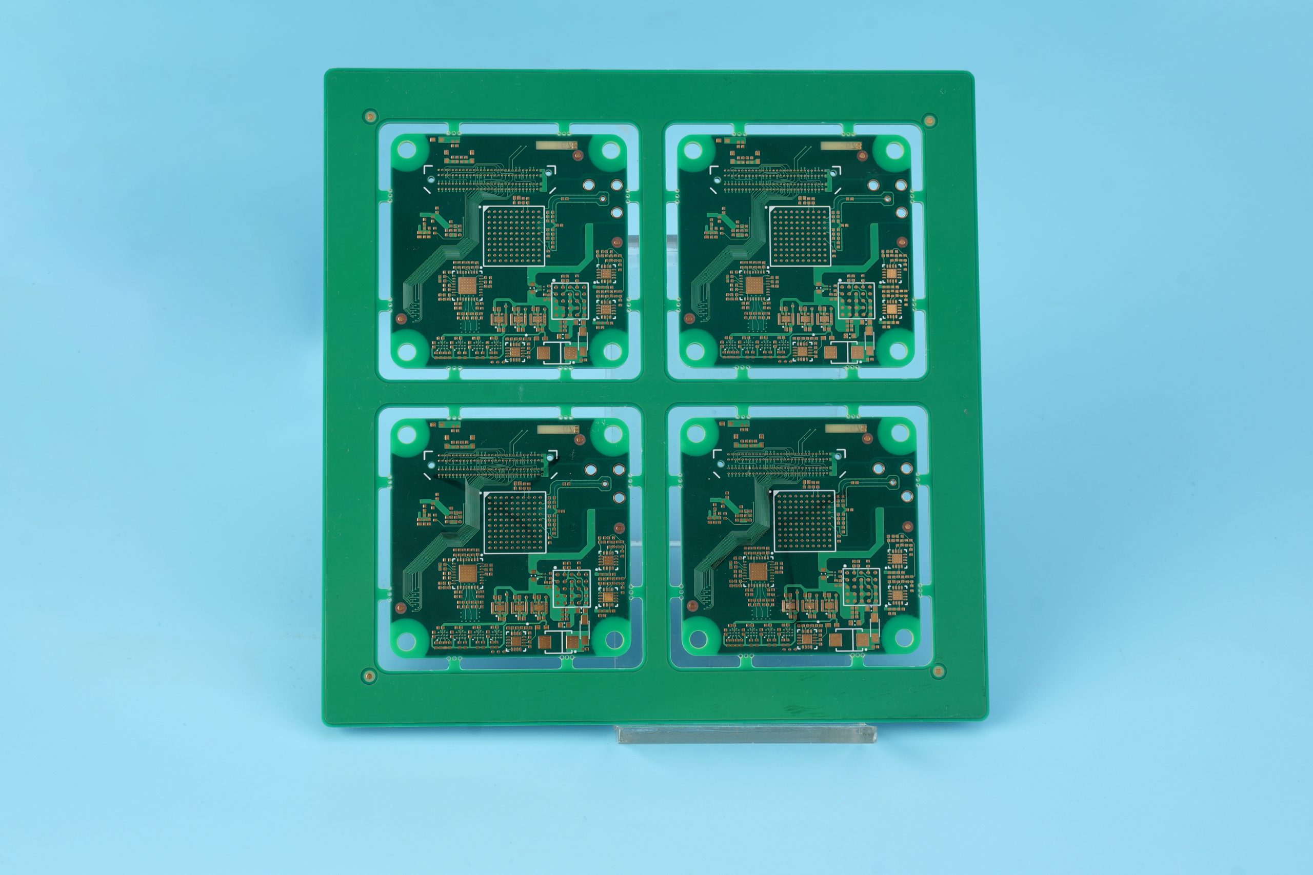
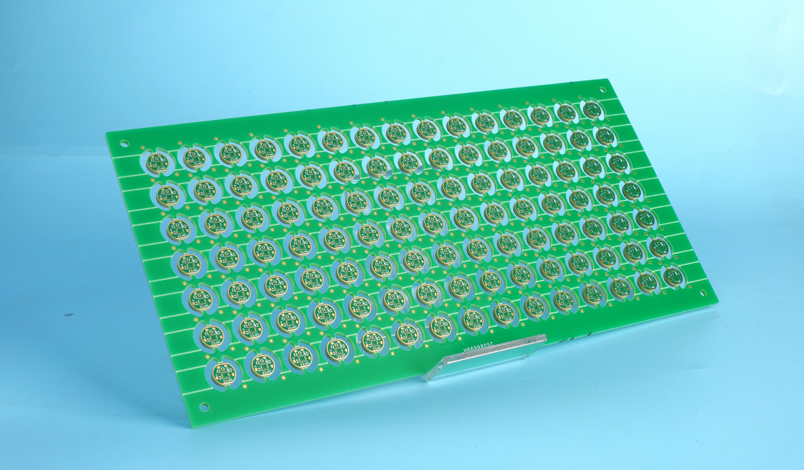
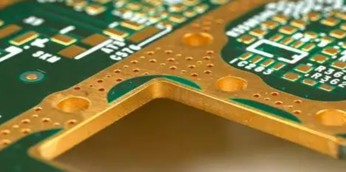
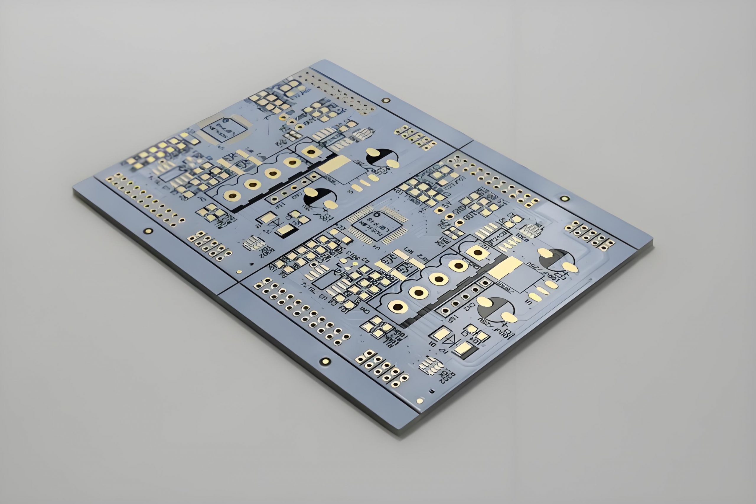
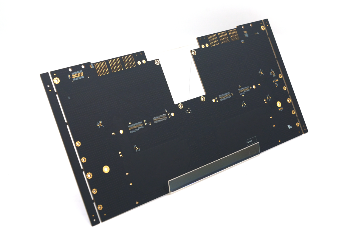
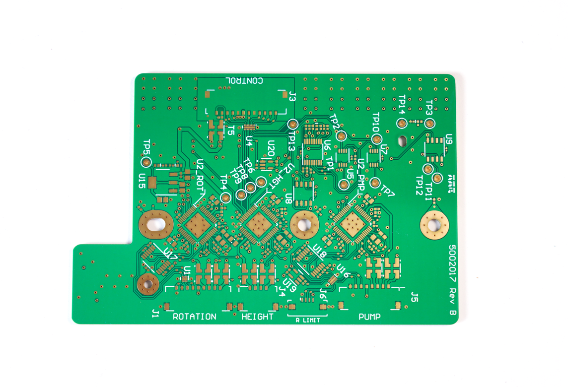
What Is PCB Fabrication?
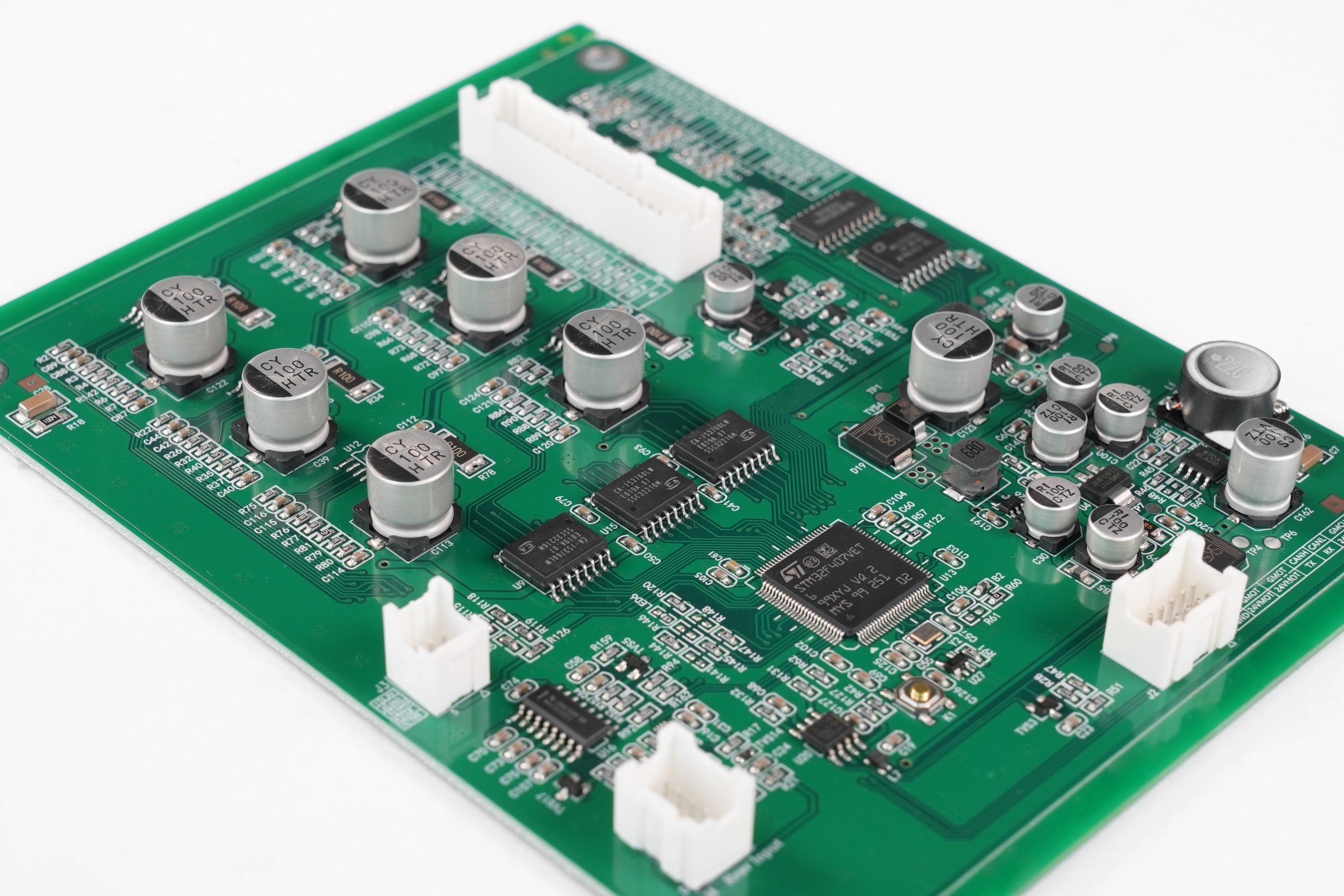
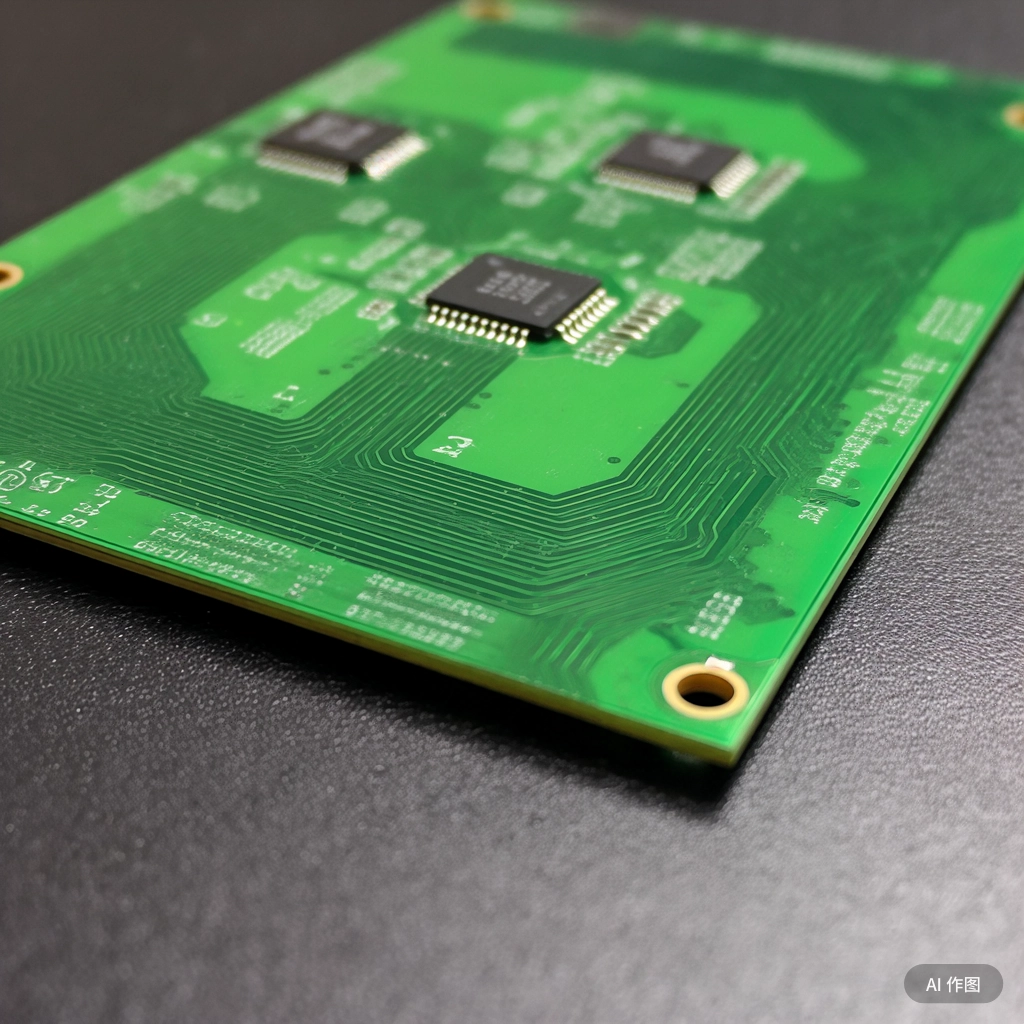
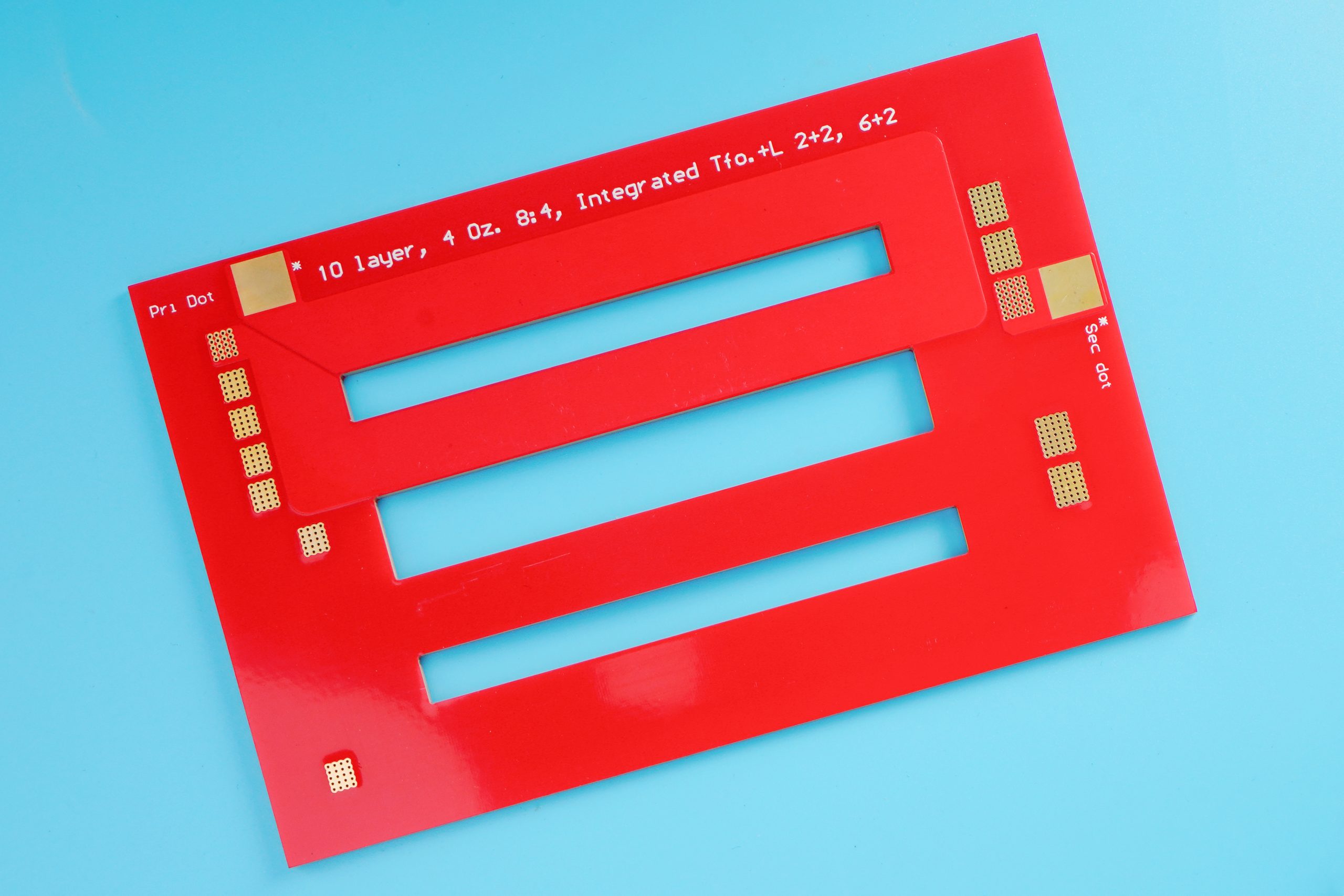
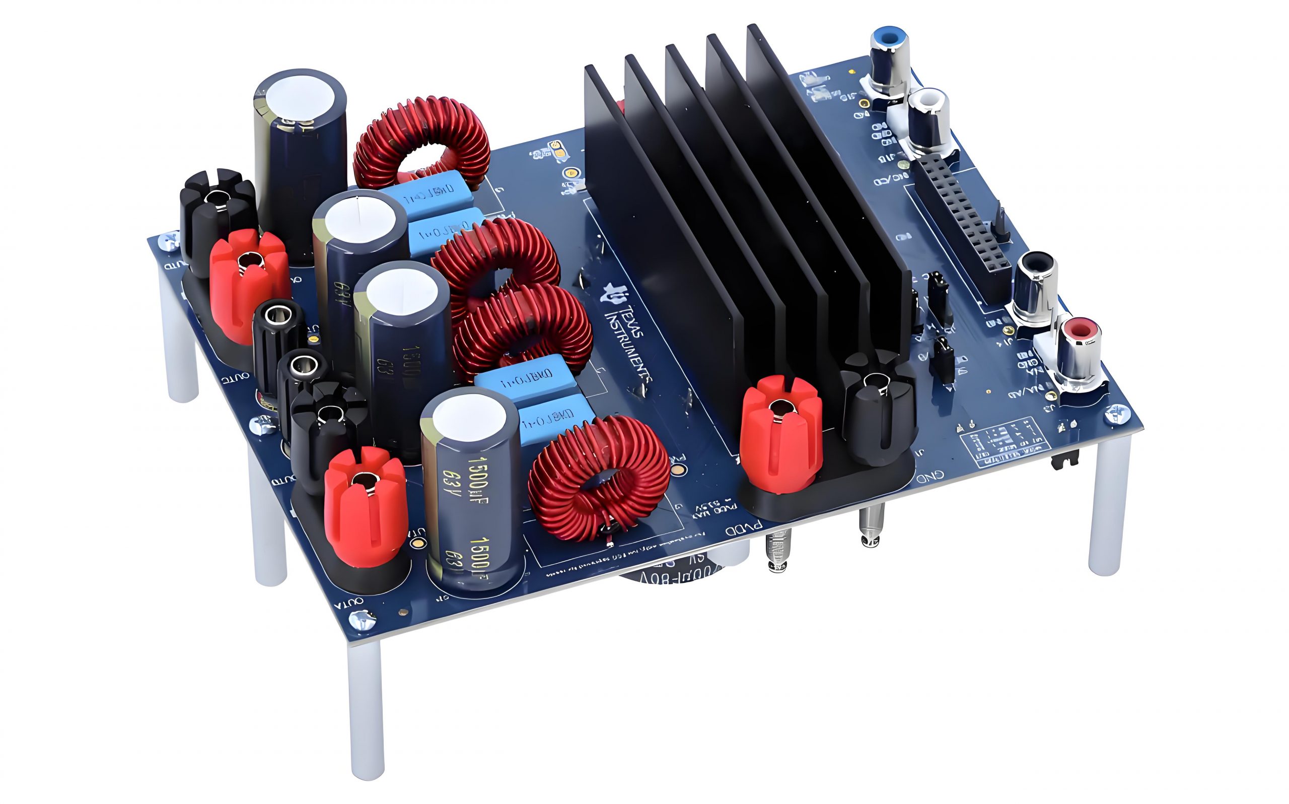
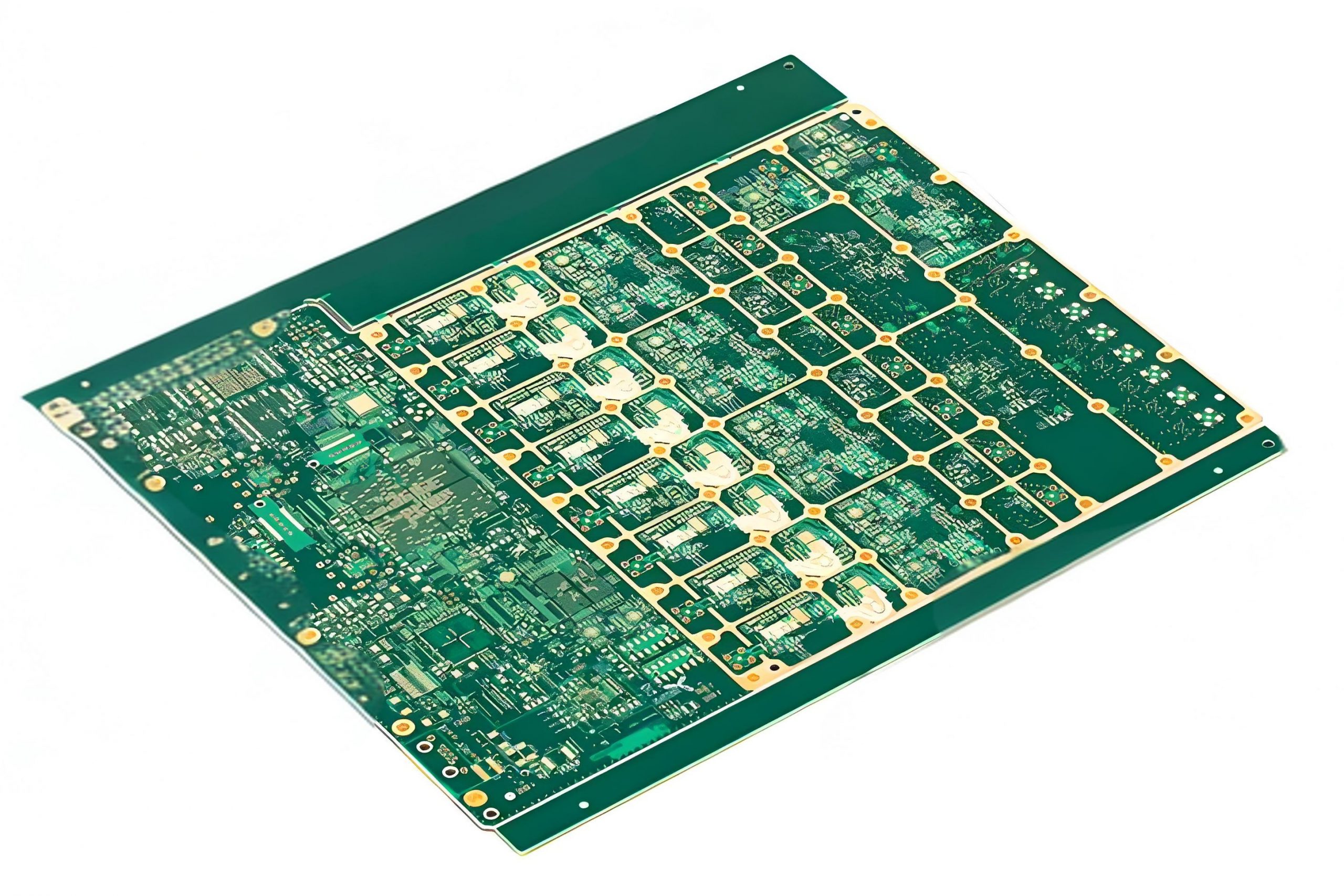
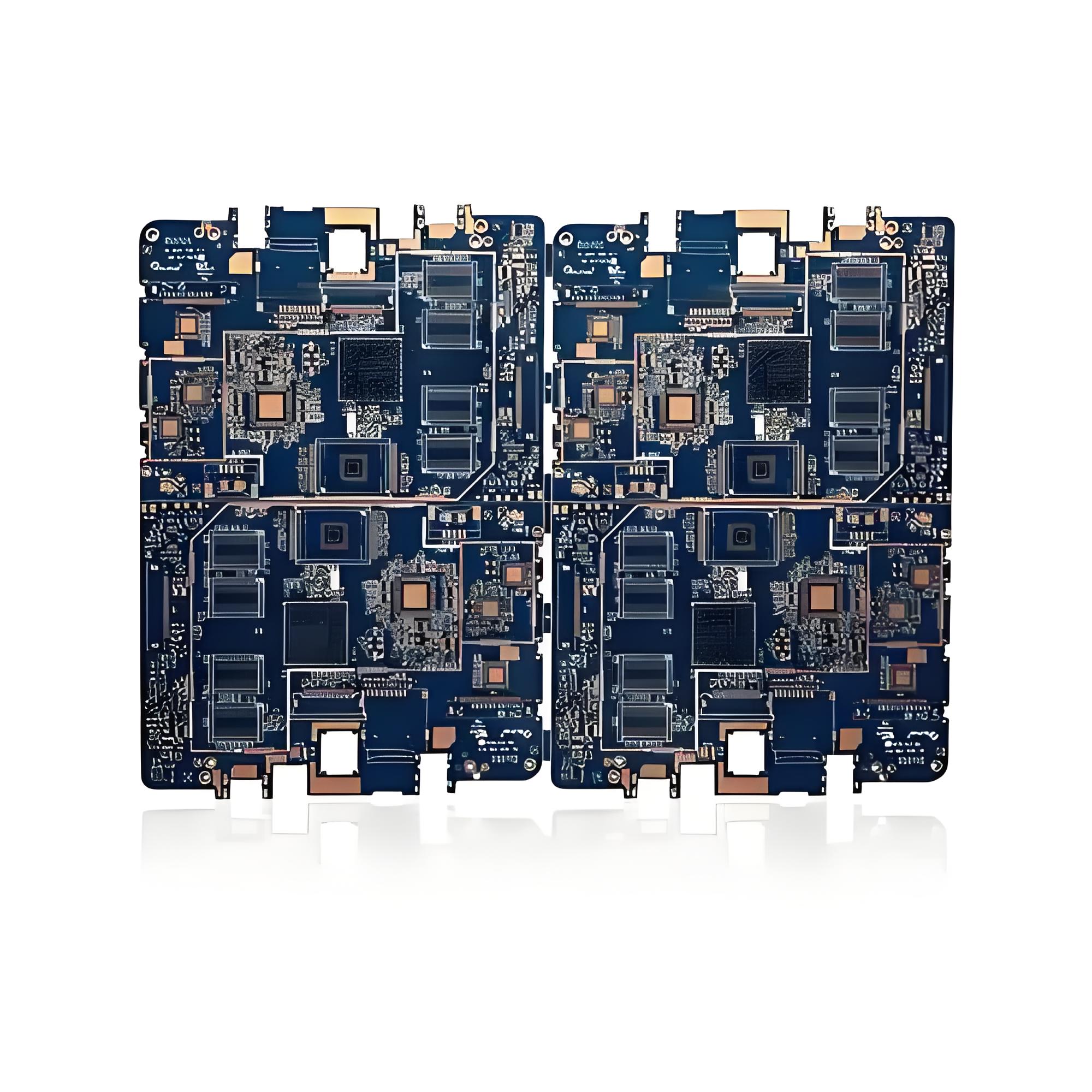
PCB fabrication is the manufacturing process that transforms circuit board designs into physical, functional products ready for component assembly. Beginning with a substrate material, the process involves precise copper patterning to create conductive pathways, followed by laminating insulating layers, drilling holes for vias and component leads, and applying protective solder mask and silkscreen. Each step requires careful attention to design specifications to ensure proper electrical connectivity, thermal management, and mechanical reliability. Advanced fabrication techniques accommodate high-density interconnects, controlled impedance for high-speed signals, and specialized materials for challenging environments. By maintaining strict quality control throughout production, manufacturers deliver boards that perform as intended while meeting cost and timeline expectations – ultimately reducing development risks for engineers and enabling smoother transitions from prototype to mass production.
How to Choose A One-Stop PCB Solution Supplier For Your PCB Fabrication Project?
Tips about one-stop PCB solution supplier selection:
- Evaluate Technical Expertise and Capabilities: Begin by assessing whether the supplier offers end-to-end services, including design assistance, prototyping, fabrication, assembly, and testing. Ensure they support your project’s complexity, whether it involves rigid boards, flex circuits, HDI, or advanced materials. A supplier with in-house engineering teams can preemptively address DFM (Design for Manufacturability) issues, saving you time and rework costs.
- Verify Quality Certifications and Standards: Prioritize suppliers with certifications like ISO 9001, IPC-A-600, and UL recognition. These certifications demonstrate adherence to global quality and safety standards, reducing the risk of defects or compliance issues. Request samples or case studies to evaluate their workmanship, especially for high-speed or high-reliability applications.
- Assess Production Capacity and Flexibility: Confirm the supplier’s ability to scale production to meet your volume needs, from prototypes to mass production. Inquire about their equipment’s precision (e.g., laser drilling for microvias) and material inventory to handle lead-free RoHS-compliant processes or specialized laminates. Flexibility in accommodating rush orders or design changes can prevent project delays.
- Compare Pricing and Transparency: Request detailed quotes that break down costs for design, materials, fabrication, assembly, and testing. Beware of hidden fees for services like stencils or impedance control. A transparent supplier will explain cost drivers, such as layer count or tight tolerances, helping you optimize design choices without sacrificing performance.
- Review Turnaround Time and Logistics: Shorten your time-to-market by choosing a supplier with fast prototyping lead times (e.g., 24–48 hours for bare boards). Inquire about their global shipping capabilities, customs clearance support, and inventory management for consigned components. A supplier with local facilities can reduce shipping costs and delivery times.
- Seek Customer References and Reviews: Contact the supplier’s existing clients to gauge their reliability, communication, and problem-solving efficiency. Look for testimonials highlighting their responsiveness during crises, such as component shortages or design emergencies. A supplier with a proven track record in your industry (e.g., automotive, medical) will better understand your regulatory needs.
- Leverage Design Support and DFM Reviews: Prioritize suppliers offering free DFM checks before fabrication. This service identifies issues like impossible trace widths, insufficient solder mask clearance, or panelization inefficiencies, preventing costly re-spins. Some suppliers also provide signal integrity simulations or thermal management guidance, adding value beyond basic manufacturing.
- Ensure Component Sourcing Reliability: If outsourcing assembly, confirm the supplier’s access to authorized component distributors to avoid counterfeit parts. Inquire about their strategies for mitigating obsolescence or supply chain disruptions, such as maintaining safety stock or cross-referencing alternatives.
How to Ensure On-Time Delivery for PCB Fabrication Orders with Complex Specifications?
Here are ways about how to speed up the process of PCB fabrication orders with complex specifications:
- Conduct a Thorough Pre-Production Technical Review: Engage your supplier early to review design files, material specifications, and tolerance requirements. A detailed technical audit identifies potential manufacturing bottlenecks, such as impossible microvia dimensions or incompatible laminate choices, before production begins. Addressing these upfront prevents costly rework later.
- Establish Clear Milestones and Deadlines: Break the project into phases (e.g., design finalization, prototyping, tooling, mass production) with defined deliverables and timelines. Use project management tools to track progress and hold regular check-ins with your supplier. Visibility into each stage ensures accountability and enables swift corrective actions if delays emerge.
- Prioritize Suppliers with Advanced Manufacturing Capabilities: Select a supplier equipped to handle complex specifications, such as HDI boards, rigid-flex designs, or embedded components. Inquire about their machinery precision (e.g., laser drills for microvias), material inventory, and experience with similar projects. A technically capable partner reduces iterations and accelerates production.
- Leverage Parallel Workstreams: Overlap non-dependent tasks to compress schedules. For example, initiate component sourcing or stencil fabrication while awaiting prototype test results. This approach minimizes idle time and keeps the project moving forward.
- Implement Real-Time Communication Channels: Establish direct, frequent communication with your supplier’s project manager via shared platforms (e.g., Slack, Microsoft Teams) or daily stand-up meetings. Immediate access to decision-makers resolves issues like design clarifications or material substitutions quickly, preventing delays from back-and-forth emails.
- Secure Component Availability Early: If outsourcing assembly, confirm component lead times and lock in orders with authorized distributors well in advance. For long-lead-time or obsolete parts, collaborate with your supplier to identify alternatives or pre-book inventory. This proactive step avoids production halts due to missing components.
- Perform Staged Quality Inspections: Schedule interim quality checks during fabrication (e.g., after layer stacking, etching, or solder mask application) rather than waiting for final inspection. Early detection of issues like layer misalignment or impedance deviations allows timely corrections without derailing the timeline.
- Build Flexibility into Logistics: Partner with logistics providers offering expedited shipping options and real-time tracking. For critical orders, negotiate guaranteed delivery windows or use air freight as a backup. Having contingency plans for customs delays or port congestion ensures shipments arrive on schedule.
How to Reduce the Cost of PCB Fabrication without Affecting Quality?
Below are methods about how to reduce the cost of PCB fabrication without affecting quality:
- Start with Layer Count Optimization: Reduce unnecessary layers by consolidating signal routes or using blind/buried vias strategically. For example, a 6-layer board might be redesigned as a 4-layer board with optimized impedance control. Collaborate with your supplier to validate stack-up changes that meet electrical needs without over-engineering.
- Maximize Panel Utilization: Arrange multiple PCB designs or array identical boards to minimize material waste. Standard panel sizes (e.g., 18×24 inches) avoid custom tooling fees. A 10% improvement in panel efficiency can lower per-unit costs by up to 15%.
- Simplify Hole and Trace Specifications: Relax tight tolerances for hole sizes or trace widths unless dictated by performance. Increasing a 0.1mm trace/space to 0.15mm reduces etching costs and improves yield. Replace plated-through holes with via-in-pad only where essential.
- Secure Volume-Based Discounts: Commit to larger batch quantities or annual forecasts to unlock tiered pricing. Suppliers often offer 10–30% discounts for orders exceeding 50–100 panels. Negotiate blanket agreements to lock in rates for recurring needs.
- Adopt Cost-Effective Surface Finishes: Choose HASL or OSP instead of ENIG for non-critical boards. These finishes balance solderability and cost, saving 10–20% per panel. Reserve premium finishes for high-wear areas like connector pins.
- Leverage Supplier DFM Expertise: Share Gerber files early for a free Design for Manufacturability (DFM) review. Suppliers may suggest tweaks like replacing gold immersion with HASL or adjusting pre-preg combinations to reduce lamination cycles.
- Consolidate Component Sourcing: Centralize component procurement with your supplier to leverage their bulk purchasing power. Avoid mixing consigned and turnkey components, which raises administrative fees. For example, consolidating 50+ components can cut sourcing costs by 5–15%.
- Reuse Test Fixtures and Stencils: Retain stencils, test jigs, and fixtures for recurring orders to avoid retooling fees. Proper storage prevents damage and ensures readiness for future runs, saving 50–200 per tool.
Conclusion
From initial PCB design to final fabrication, every phase demands precision to avoid costly delays and ensure optimal performance. Implementing structured design validation, material optimization, and streamlined workflows can significantly enhance both quality and efficiency. For projects requiring integrated solutions from thermal management in metal PCBs to high-frequency signal integrity—EBest Circuit (Best Technology) offers comprehensive expertise in bridging design intent with manufacturing execution. Contact us today for a customized quotation that aligns with your technical specifications and budget constraints. Let’s transform your concepts into reliable PCBs with our end-to-end capabilities, rigorous quality control, and commitment to on-time delivery: sales@bestpcbs.com.