Why choose high dielectric PCB material? Let’s discover its definition, material list and properties, benefits, selection guide, cost and recommend material supplier through this blog.
Are you troubled with these problems?
Is high-frequency signal instability plaguing your designs? Could PCB dielectric constant fluctuations be causing impedance mismatch?
Struggling with cost containment? Has the price surge of high-Dk materials disrupted your inventory planning?
Is sample testing taking too long? Can you receive small-batch verification materials within 72 hours?
As a high dielectric PCB material supplier, EBest Circuit (Best Technology) can provide you service and solutions:
Precise Dk/Df parameter matching: Full Rogers/Taconic inventory with 24-hour parameter traceability to eliminate design validation discrepancies.
Price volatility buffer: Long-term agreements lock in costs, with off-season stock support and peak-season priority allocation.
Sample readiness: 72-hour rapid slicing and delivery with batch-specific COA reports to accelerate design iterations.
Welcome to contact us if you have any inquiry for high dielectric PCB materials: sales@bestpcbs.com.
What is High Dielectric PCB Material?
High Dielectric PCB Material(High Dk PCB) refers to specialized substrate materials engineered for high-frequency circuit applications (typically >1 GHz), characterized by two core attributes: high dielectric constant (Dk > 10) to enable compact signal transmission structures, and low dielectric loss (Df < 0.01) to minimize signal attenuation.
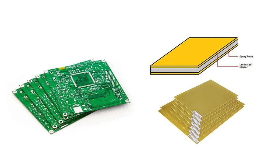
These materials are typically formulated using polytetrafluoroethylene (PTFE)-ceramic composites, hydrocarbon resins, or modified epoxy resins, with ceramic powders (such as barium titanate) incorporated to enhance dielectric performance. Such materials are particularly suitable for applications requiring miniaturization and high-frequency stability, including millimeter-wave radar systems and 5G base stations, where both compact design and signal integrity are critical.
High Dielectric Constant PCB Material List & Properties
Hybrid Laminate: High-frequency signal layers use premium materials (e.g., RO4350B), while inner power/ground planes use FR4 to balance cost/performance.
Thermal Solutions: Metal-core boards + high-frequency dielectric layers, paired with thermal vias (diameter ≥0.3mm) for efficient heat dissipation.
Drilling & Plating: Laser-drilled microvias (≤0.15mm) with electroplated fill avoid burrs and reflections; hole wall roughness ≤20μm.
5. Supply Chain & Cost Considerations
Domestic Material Alternatives: Shengyi S7G series offers Df ≤0.004 at 10GHz, 30% lower cost than imports, suitable for mid-high frequency applications.
Lead Time Management: High-frequency substrates require 3-6 months advance procurement; RO4350B has stable inventory, while PTFE needs custom production (8-12 weeks).
Environmental Compliance: RoHS and halogen-free compliance; ≥20% recycled content aligns with sustainability trends (e.g., ISO 14001-certified materials).
How Much Does High Dielectric PCB Material Cost?
Material Type
Price Range (USD)
Representative Model
Standard FR4
5-8
IS410/IT180A
Modified Epoxy Resin
15-25
Nelco N4000-13
Ceramic Filled Substrate
40-70
Rogers RO4350B
PTFE High Frequency Material
80-180
Rogers RT/duroid 6002
Special Composite Material
200-350
Taconic RF-35A2 (Copper included)
Why Choose EBest Circuit (Best Technology) as High Dielectric PCB Material Supplier?
Material Performance Validation Package: Third-party certified dielectric/loss factor reports ensure precise parameter matching with design specs, eliminating guesswork in high-frequency PCB development.
Eco-Compliance Solutions: RoHS/REACH dual-certified substrates enable seamless EU/NA market entry while boosting green brand value through regulatory compliance.
Cost Optimization Algorithms: Proprietary stack-up design reduces BOM costs by 10-18% without compromising performance, maximizing profit margins.
Failure Analysis Center: SEM/X-ray labs cut pilot production yield loss by 15% through root-cause diagnosis, minimizing trial costs.
RF Application Database: 3000+ proven RF module designs provide turnkey reference from material selection to circuit layout, accelerating time-to-market.
24/7 Technical Support: 4h response/24h solution delivery by senior engineers resolves material application challenges, ensuring project continuity.
Dielectric Constant Calibration: Precision tuning of dielectric properties for 5G/mmWave applications achieves 20% signal loss reduction, enhancing product competitiveness.
Global Logistics Network: 48-hour rapid prototyping delivery supported by strategic inventory minimizes R&D cycle delays.
How to Get a Quote for High Dielectric PCB Material?
High-Dielectric PCB Material Quotation Request Checklist
1. Basic Technical Parameters
Dielectric Constant (Dk) Range: Specify exact range (e.g., Dk=3.0±0.05)
Loss Tangent (Df) Requirement: e.g., Df≤0.003@10GHz
Substrate Model: Include brand/model (e.g., Rogers RO4350B, Taconic RF-35)
What is small PCB board? Let’s explore its definition, benefits, applications, design spec and guide, production process and recommended PCB manufacturer through this blog.
Are you troubled with these problems?
How to fit multi-modules (sensors + 5G) in wearables without compromising performance?
How to ensure stable signals for 5G/AR modules with micro-scale traces?
How to prevent thermal failure in compact devices like drones/medical portables?
As a professional small PCB manufacturer, we can provide you service and solutions:
Space Optimization: Micron-scale HDI routing and 4-layer stackup integrate controller, sensor, and Bluetooth within 20cm² with 40% density improvement.
Signal Stability: Routing simulation and arc transitions reduce 5G module delay by 20% and crosstalk by 15dB.
Thermal Control: High-density thermal vias and heat channels limit temperature rise to ≤30°C with 25% efficiency gain.
Compact PCB challenges solved with three key solutions precise routing, stable signals, optimized thermal management.
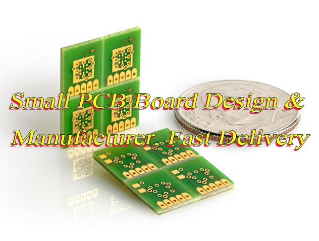
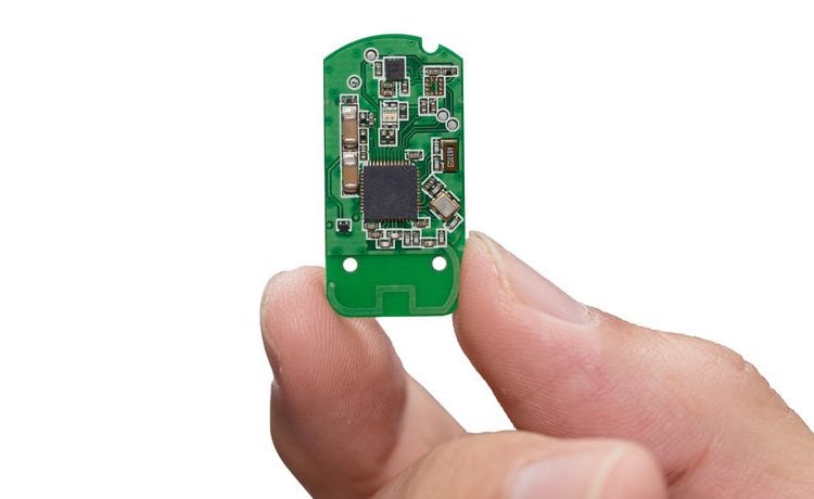
Small PCB Boardrefers to a printed circuit board designed with significantly reduced physical dimensions (typically under 20 cm² in area or with any side ≤50 mm) to fit space-constrained applications, while integrating essential electronic components and conductive pathways to enable specific functionalities within compact devices like wearables, medical implants, or micro-sensors. Its miniaturization necessitates specialized manufacturing techniques, such as high-density interconnect (HDI), laser micro-vias, and precise impedance control to maintain electrical performance despite stringent size limitations.
What Are Benefits of Small Circuit Board?
Space Utilization Optimization
Minimize equipment size to meet rigid compact layout requirements for wearables/IoT modules.
Multi-layer stack design enables complex functions within limited area, reducing overall system footprint.
Signal Integrity Enhancement
Shortened trace length reduces signal delay/crosstalk, ideal for high-frequency circuits (e.g., 5G/RF modules).
1. Precision Dimension Control & Tolerance Verification
Outline Size Standards: Strict adherence to ≤20cm² limits (e.g., 10mm×10mm smartwatch mainboards) with 0.1-1.2mm ultra-thin substrates (FR4-Tg170+), validated by IPC-2221 ±0.1mm tolerance. Case: Medical implants achieve seamless tissue integration via 0.2mm tolerance control.
3D Space Optimization: MCAD tools (SolidWorks) ensure ≥0.5mm clearance between PCB/housing/batteries, preventing assembly stress-induced cracks.
2. Stackup Optimization & Simulation Validation
Stackup Strategy: 4-layer “Signal-GND-Power-Signal” reduces HF crosstalk by 40% (5G module validation data); 8-layer expands to “Signal-GND-Signal-Power-GND-Signal-GND-Signal” for multi-channel radar units.
HDI Microvia Application: 0.1mm/0.08mm trace/space via laser-drilled 0.1mm microvias, paired with blind/buried vias to enhance routing density. Example: AR glasses driver boards achieve 3× density increase and 20% latency reduction via HDI.
3. Impedance & Signal Integrity Refinement
Control Standards: 50Ω±10%@900MHz (TDR error ≤5%), differential 100Ω±5%; length matching ≤5mil (0.127mm) prevents timing skew. Case: UHF RFID read range improved by 30% via impedance tuning.
Mounting Holes: ±0.1mm tolerance, IEC 60068-2-27 shock test (500g/1ms); -40℃~125℃ range with 85℃/85%RH/1000h and -55℃~125℃/500-cycle tests.
Certifications: ISO 13485 (medical), AEC-Q100 Grade 1 (automotive), IEC 60947 (industrial). Example: ADAS modules achieve decade-long fault-free operation via AEC-Q100.
How to Make a Small Printed Circuit Board?
1. Circuit Design and File Generation
Using EDA software (e.g., Altium Designer 23, KiCad) to complete schematic design and PCB layout, generating Gerber files containing circuit, drilling, and solder mask information. DFM review ensures compliance with IPC-A-600 standards, including minimum trace width (6mil/0.153mm), spacing (8mil/0.2mm), and hole size tolerance (±0.05mm).
2. Substrate Preparation and Cutting
Select FR-4 epoxy glass cloth substrate (IPC-4101 certified) based on application requirements. Cut large copper-clad laminate to design size using precision shearing machines. Perform mechanical/chemical cleaning (e.g., pumice scrubbing) to remove oxidation and ensure surface adhesion for subsequent processes.
3. Inner Layer Circuit Formation
Apply dry film photoresist on copper-clad board, transfer design patterns via UV exposure (365nm wavelength, 10-20mJ/cm? energy). Develop to remove unexposed areas, etch unprotected copper using ferric chloride solution, then strip residual film. AOI inspection detects defects like shorts/opens with 5μm resolution.
4. Lamination and Stacking
After browning treatment (copper surface oxidation to enhance bonding), alternate core boards and prepreg (PP) sheets. Stack with copper foil outer layers, press under vacuum/hot-press (180-200℃, 300-500psi pressure) to achieve layer bonding and curing. Semi-cured epoxy resin forms insulated interlayer connections.
5. Drilling and Hole Metallization
Mechanical/laser drilling creates through-holes/blind vias (diameter down to 0.1mm). Hole wall metallization involves chemical copper deposition (0.3-1μm thin layer) followed by electroplating to 20-25μm thickness. X-ray drilling ensures positional accuracy ±0.05mm.
Apply epoxy ink (e.g., green solder mask) via screen printing, expose/develop to open pad windows. Surface finishes include HASL (tin/lead), ENIG (immersion gold), or OSP (organic solderability preservative) to enhance solderability and corrosion resistance.
8. Silkscreen and Profiling
Screen-print component markings/logos using UV-curable ink (≥6mil/0.153mm line width). Profile cutting via CNC routing or V-scoring (depth control ±0.1mm) ensures panel separation with smooth edges.
9. Electrical Testing and Inspection
Conduct continuity/insulation testing using flying probe/ICT fixtures. AOI/AXI detects defects like missing pads/solder bridges. Final checks include dimensional verification (calipers/CMM), impedance testing (±10% tolerance), and thermal shock testing per IPC-TM-650.
10. Packaging and Shipping
After ultrasonic cleaning and baking, boards undergo vacuum packaging with desiccant and humidity indicator cards. Labels include batch number, production date, and QA certification. Ships in ESD-safe containers compliant with RoHS/REACH standards.
Why Choose EBest Circuit (Best Technology) as Small PCB Board Manufacturer?
Cost Optimization Solution: By optimizing material selection and process pathways, we reduce production costs for small and medium batch orders by 12%-18%. Combined with a dynamic cost accounting system, we deliver cost-sensitive design solutions for clients. This has helped over 300 customers achieve an average annual manufacturing cost savings of 15%.
Rapid Prototyping System: Urgent orders support 24-hour rapid prototyping. Leveraging dual-shift production lines and intelligent scheduling systems, we compress the industry-average 48-hour prototyping cycle by 50%. 2024 data shows over 85% of expedited orders complete prototype verification on the same day, accelerating product iteration efficiency.
On-Time Delivery Guarantee: 99.2% on-time delivery rate, verified by ISO 22483 supply chain management certification, significantly outperforms the industry average of 95%. Through AI-driven production forecasting and dynamic inventory allocation, Q3 2025 data indicates over 98% of orders are delivered ahead of schedule or on time, enhancing client supply chain stability by 40%.
Full-Inspection Quality Control: Batch orders undergo 100% full inspection using AOI and X-ray dual inspection systems, achieving a defect detection rate of 99.2%. Compared to manual sampling, efficiency improves by 300%. 2024 customer return rates remain below 0.03%, far below the industry average of 0.5%.
Authoritative Certification System: Certifications include ISO 9001:2015, IATF 16949:2016 automotive-grade, medical ISO 13485, and RoHS 2.0 lead-free compliance. Covering high-compliance sectors like automotive electronics, medical devices, and industrial control, we added EU CE-RED wireless device certification in 2025 to meet global market access requirements.
Experience-Based Knowledge System: Built on 19 years of PCB production data, our error database contains over 200,000 process defect cases and solutions. AI-driven analysis identifies 85% of design risks in advance, reducing client trial-stage problem-solving time by 40% and minimizing repeated trial costs.
Free DFM Analysis: Complimentary Design for Manufacturability (DFM) analysis combines EDA tools with engineering expertise to identify design flaws like trace width/spacing violations and impedance mismatches early. 2024 data shows DFM reduces client design revisions by 45% and shortens product launch cycles by an average of 21 days.
End-to-End Service Chain: Integrating design consulting, prototyping, SMT assembly, functional testing, and logistics through an ERP system for real-time order tracking. Clients reduce supply chain management costs by 25% and improve coordination efficiency by 30%, ideal for multi-SKU small-batch orders.
Welcome to contact us if you have any inquiry for small PCB board: sales@bestpcbs.com.
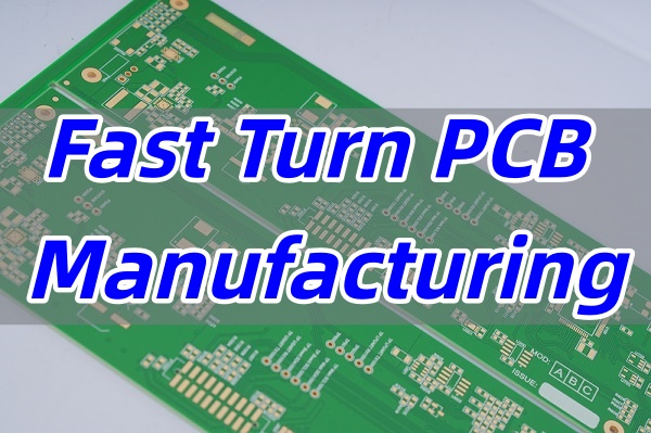
Fast turn PCB manufacturing is at the heart of modern electronics, where speed, precision, and reliability are critical. This blog provides a comprehensive guide on fast-turn PCB, covering its definition, cost structure, quality assurance, testing methods, production lead time, manufacturer selection, and turnkey PCB services in China, helping readers understand how to efficiently obtain high-quality PCBs.
Do you encounter any of the following challenges in fast turn PCB manufacturing?
Signal Integrity Control: Precision routing and multilayer design for stable performance.
High-Quality Materials & Processes: Premium substrates and efficient workflows.
Cost & Efficiency Optimization: MES system enables fast iteration with controlled costs.
As a leading quick turn PCB manufacturer in China, EBest Circuit (Best Technology) excels in delivering high-quality, fast-turn PCB solutions. We offer comprehensive services including rapid prototyping, PCB fabrication, assembly, and turnkey solutions across a wide range of boards such as FR4, flexible circuits, rigid-flex, aluminum, and ceramic substrates. For professional consultation or inquiries, please contact us at +86-755-2909-1601 or sales@bestpcbs.com, and our team will be happy to assist you.
What is a Fast Turn PCB Manufacturing?
Fast turn PCB manufacturing is fundamentally a PCB production service that prioritizes lead time above all else. It focuses on rapid fabrication, quick assembly, and prompt delivery while maintaining strict standards for performance and reliability. Its main goal is to provide time assurance for R&D, urgent production needs, and small-batch pilot runs, helping companies gain an edge in product development and market responsiveness.
Why Fast Turn Services Are Needed — Three Core Values
Accelerating R&D Iteration: Engineers can quickly obtain prototypes to validate circuit design, component layout, and functionality. This rapid iteration reduces waiting time for revisions and accelerates product optimization.
Meeting Urgent Market Demands: Whether for sample demonstrations, production replenishment, or seizing market opportunities, fast turn PCBs deliver quickly, ensuring companies do not miss critical windows.
Controlling Project Risk and Cost: Small-batch pilot runs help identify design flaws before large-scale production, reducing expensive rework. Early validation also optimizes material usage and manufacturing processes, lowering overall project cost.
Fast turn PCB lead times generally fall into several common ranges:
24 hours: Suitable for single-sided or simple double-sided prototypes.
48 hours: Medium complexity, multi-layer prototypes.
72 hours: Complex multi-layer boards for small batch pilot production.
5 days: High-density, multi-layer boards for small batch production.
Note: Lead time starts after order confirmation and data review. Actual timing may vary depending on layer count, board material, and complexity.
Difference Between Fast Turn and Standard PCBs
Feature
Fast Turn PCB
Standard PCB
Purpose
Short lead time, rapid iteration
Cost optimization, stable production
Lead Time
1-5 days
7-20 days
Application Stage
Prototyping, small batch pilot
Mass production
Ultimately, fast turn does not mean compromising standards. Through optimized processes, advanced equipment, and strict quality systems, every board maintains high reliability. Even under the fastest turnaround, PCBs undergo essential electrical and reliability testing. Fast turn PCB manufacturing is not only a tool to speed production but a strategic asset for product development.
What is Fast Turn PCB Manufacturing Cost?
Fast turn PCB costs are not fixed numbers—they fluctuate dynamically based on multiple factors. Understanding what drives pricing is key for making informed decisions. This section breaks down the seven core cost drivers and provides practical tips to control expenses, helping you plan your budget wisely. A simple way to think about the total cost is:
Total Cost = Material Cost + Process Complexity Cost + Expedited Fee + Quality Assurance Cost ± Order Scale Effect
Each component reflects a specific investment in time, precision, and reliability.
a) Material and Base Parameters (“Ingredients”)
Board Size and Quantity: Larger boards generally cost more per piece, but increasing quantity can reduce unit cost due to economies of scale. Understanding the non-linear relationship helps optimize orders.
Number of Layers: Each additional layer significantly increases cost, due to alignment and lamination complexity.
Board Material: FR-4, high-frequency materials (Rogers), aluminum, and flexible substrates have different price ranges. Selection depends on performance requirements and application.
b) Process Complexity (“Cooking Difficulty”)
Trace Width and Spacing: Finer traces demand higher precision and specialized equipment, raising costs.
Minimum Hole Size and Number of Holes: Drilling is labor and time-intensive. Smaller and more numerous holes increase manufacturing expense.
Surface Finish: HASL, ENIG, ENEPIG, and gold plating have varying costs and suit different applications.
Special Processes: Blind/buried vias, impedance control, and other advanced techniques add cost due to extra steps and testing requirements.
c) Expedited Fee (“Speed Premium”)
Expedited fees are not arbitrary—they cover:
Dedicated Production Capacity: Orders may interrupt or bypass standard queues.
Extra Labor: Overtime for engineering review, manufacturing, and inspection.
Express Logistics: Air shipping is often necessary for 24-48 hour delivery instead of standard sea or land transport.
Example: A 48-hour delivery can be 30%-50% more expensive than a standard 7-day lead time. This provides a tangible perspective for clients.
d) Quality Assurance Cost (“Insurance Premium”)
Standard fast turn PCBs include AOI and flying probe tests. More rigorous full-process electrical testing may add cost but prevents costly failures later. Investing in QA protects both product reliability and brand reputation.
How to Control Costs Effectively?
Optimize Design: Use standard hole sizes, slightly increase trace width and spacing, and minimize via count where possible.
Select Appropriate Processes: Stick to standard FR-4 and ENIG finishes unless higher-spec materials are necessary.
Plan Lead Times Strategically: Longer but still fast lead times (e.g., 5-7 days) are significantly cheaper than 24-48 hour rush orders.
Consolidate Orders: Place multiple small prototypes on one panel and cut after production. This approach lowers unit cost and reduces waste.
In essence, understanding the structure behind fast turn PCB costs gives you three advantages:
Clarity: You know where your money goes.
Control: You can adjust design or lead time to influence costs.
Trust: Transparent cost breakdown demonstrates professionalism and reliability.
How to Ensure Quality During Manufacturing PCB Process?
Implementing these tests allows EBest Circuit (Best Technology) to ensure high reliability and minimize post-production failures, addressing critical concerns for clients in high-stakes industries.
How to Find Fast Turn Printed Circuit Board Manufacturers?
Finding a reliable fast turn PCB manufacturer requires more than browsing a list of suppliers. The right choice ensures your project meets deadlines, maintains quality, and avoids costly rework. This guide outlines efficient channels and actionable evaluation tips to help you locate genuine fast-turn partners.
1. Online Channels – Fastest and Most Direct
Search Engines (Google, Bing, etc.)
Use targeted keyword combinations instead of generic searches like “PCB manufacturer”:
"fast turn PCB"
"quick turn PCB prototype"
"24 hour PCB assembly"
"China PCB quickturn" (for sourcing from China)
Pro tip: Check the first few pages of search results. Top-ranking websites often reflect strong online presence and operational professionalism.
Professional B2B Platforms & Industry Directories
Global B2B platforms like ThomasNet or Alibaba can provide verified company listings.
Electronics forums (e.g., EEVblog, Electro-Tech-Online) often feature engineer discussions and recommendations—valuable for real-world supplier feedback.
Professional Social Networks (LinkedIn, Industry Groups)
Search "PCB manufacturing" to find company pages and sales contacts.
Join industry-specific LinkedIn groups to observe active suppliers and post inquiry requests.
2. Offline & Indirect Channels – Cross-Verification for Premium Suppliers
Industry Trade Shows
Attend large electronics events such as NEPCON or APEX. This allows face-to-face evaluation of multiple suppliers’ technical capabilities and team professionalism.
Peer Recommendations
Ask colleagues or industry contacts about fast-turn PCB suppliers they’ve successfully worked with. Recommendations from trusted professionals are often the most reliable.
Once you have a list of potential companies, use these criteria to assess professionalism:
Website & Digital Presence
Does the manufacturer offer online quoting/order systems? Automated systems typically indicate faster internal processes.
Are fast-turn options clearly listed (24h, 48h, 72h)?
Is the website professional, transparent, and informative?
Communication & Responsiveness
Conduct a test inquiry: send your Gerber files to 2-3 shortlisted suppliers.
Evaluate their responses:
Speed: How quickly do they reply? Top fast-turn manufacturers respond rapidly.
Professionalism: Are replies clear, structured, and helpful? Do they provide preliminary DFM suggestions?
Technical Questions: Suppliers asking insightful questions about your design often indicate high expertise.
4. Recommended Sourcing Workflow
First Round (Online Search): Compile 5–10 potential suppliers via search engines, B2B platforms, and LinkedIn.
Second Round (Website Screening): Visit their websites and apply the core evaluation points to narrow down to 3–5 candidates.
Third Round (Test Inquiry): Send the same Gerber file to these 3–5 suppliers, request quotes, lead times, and DFM feedback.
Final Decision: Compare pricing, communication quality, technical professionalism, and trust feeling to select your ideal partner.
By following this structured approach, you not only identify suppliers capable of fast turn PCB production but also reduce risk and gain confidence in their ability to deliver high-quality prototypes or urgent orders.
How Long Does It Take to Manufacture PCB?
PCB manufacturing time is not a fixed number. From 24-hour rapid prototypes to multi-layer boards requiring several weeks, the production cycle is dynamically determined by design complexity, chosen processes, order quantity, and supplier capability. As a manufacturer, we aim to give you transparency into the production workflow and show how we compress lead times while maintaining quality.
1. Full Breakdown: The PCB Production Flow
Pre-Engineering (6–24h) – Design review, DFM analysis, and MI creation; urgent orders prioritized for 2–4h completion.
Material Preparation (1–3d) – Boards and chemicals sourced from stock to eliminate waiting.
Electrical Testing (4–8h) – Flying probe and bed-of-nails tests prioritized.
Final Inspection (2–4h) – Appearance and dimension checks in fast-turn lane.
Board Profiling (4–8h) – CNC routing or V-Cut done first for urgent orders.
Fast-turn efficiency comes from dedicated lines, priority scheduling, and material readiness, not by compromising quality.
2. Four Key Factors That Affect PCB Lead Time
Design Complexity
Number of layers: 4-layer boards take longer than 2-layer boards.
Special features: Blind/buried vias, impedance control, or HDI structures increase processing steps and time.
Supplier Operational Model
Dedicated fast-turn production lines prevent urgent orders from waiting behind mass production.
Automated engineering review and efficient material management shorten internal delays.
Order Quantity
Small prototypes (1–10 boards) are mostly limited by setup and process time.
Large batches (hundreds or thousands) naturally take longer due to repeat processes and equipment capacity.
Logistics Time
Total time = manufacturing cycle + shipping
Air shipping vs. express vs. standard courier will significantly affect when the board reaches you.
3. How to Reduce Lead Time
During Design: Ensure DFM compliance; provide complete, accurate files to avoid rework.
During Communication: Respond promptly to the engineering queries; faster feedback shortens production delays.
When Ordering: Confirm with the supplier if they have dedicated fast-turn lines and whether your order might be queued behind mass production.
Where to Get Turnkey PCB Manufacturing in China?
Finding a reliable turnkey PCB manufacturer in China can be challenging due to the abundance of suppliers with varying capabilities. At EBest Circuit (Best Technology), we specialize in delivering complete PCB solutions that cover design support, prototyping, volume production, assembly, and testing. Here’s why partnering with us ensures a smooth, efficient, and high-quality turnkey experience.
1. Comprehensive Turnkey Services
We provide full-service PCB manufacturing, from sourcing components to final assembly and testing. Our team handles all aspects of the process, ensuring seamless integration between PCB fabrication and assembly. Clients can focus on product development while we manage the production chain efficiently.
Quality is embedded in every stage of our process. From incoming material inspection to in-line AOI, flying probe tests, and final functional testing, we maintain strict standards to deliver reliable, high-performance PCBs. Our ISO 9001, IATF 16949, ISO13485, and AS9100D certifications reflect our commitment to excellence across industries.
4. Transparent and Efficient Project Management
Clients enjoy real-time updates on production status through our MES system. Our engineers provide professional DFM reviews, risk assessment, and proactive communication to prevent delays or quality issues. This transparency builds trust and minimizes surprises throughout the project lifecycle.
5. Competitive Lead Times and Cost Efficiency
With dedicated fast-turn production lines and intelligent material management, we can deliver rapid prototypes in as little as 24–48 hours. Additionally, our ability to consolidate orders, optimize layouts, and manage supply chains reduces costs without compromising quality.
In conclusion, at EBest Circuit (Best Technology), turnkey PCB manufacturing is not just a service—it’s a complete solution designed to streamline production, ensure quality, and meet your project timelines. By choosing us, you gain a partner that combines advanced capabilities, stringent quality standards, transparent project management, and competitive lead times to help you succeed in the global market.
Cases of Fast PCB Manufacturing in EBest Circuit (Best Technology)
In the field of motion analysis and biomechanics research, precision electronic walkway systems require highly specialized printed circuit boards to ensure accurate data acquisition. EBest Circuit (Best Technology) had the privilege of providing critical PCB solutions for a leading motion analysis equipment manufacturer, supporting the performance optimization of their high-end electronic walkway products.
Technical Challenges and Solutions
Challenge: The walkway system needs to monitor and record the status of hundreds of pressure sensors in real time, placing stringent demands on PCB signal integrity, stability, and precision.
Solution:
High-Density Interconnect Design: Precision routing ensures accurate transmission of data from densely packed sensor arrays.
Impedance Control: Strictly controlled impedance matching guarantees high-speed signal integrity.
Multi-Layer Board Structure: Complex power and ground plane designs reduce signal interference.
High-Quality Materials: Premium substrates and surface finishes ensure long-term reliability.
Application Outcomes
With EBest Circuit (Best Technology)’s fast-turn PCB manufacturing services, the client’s electronic walkway system achieved:
Accurate sampling rate up to 120Hz
Spatial resolution precision of 0.5 inches
Precise detection across 16 pressure levels
Stable long-term operational performance
Excellent electromagnetic interference resistance
This case demonstrates EBest Circuit (Best Technology)’s expertise in manufacturing PCBs for high-end medical and research devices. Our solutions not only met the client’s strict requirements for precision and reliability but also provided robust technical support to enhance their competitive advantage in the motion analysis market.
All in all, fast turn PCB manufacturing is critical for businesses navigating tight deadlines, complex designs, and high-quality expectations. EBest Circuit (Best Technology) addresses common customer pain points by offering rapid prototyping, turnkey solutions, rigorous testing, and MES-enabled traceability. Pls contact us at sales@bestpcbs.com for inquiries or further details.
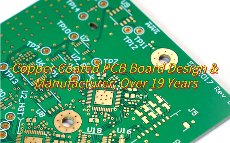
What is copper coated PCB board? Let’s explore its meaning, benefits, applications, design guide and consideration, production process through this blog.
Are you worried about these problems?
Copper Oxidation in Standard PCBs: How to ensure long-term conductivity stability?
High-Frequency Signal Loss: How to enhance copper foil adhesion and reduce impedance?
High Cost for Small-Batch Customization: Can cost-effectiveness and fast delivery coexist?
As a copper coated PCB manufacturer, EBest Circuit (Best Technology) can provide service and solutions:
Anti-Oxidation Copper Coating: Nano-scale sealing process improves oxidation resistance by 300%, with conductivity decay <2% over 5 years.
Dynamic Lamination Technology: Gradient temperature control achieves 1.5N/mm² copper-to-substrate adhesion, reducing high-frequency signal loss by 40%.
Flexible Supply Chain: 24 hours rapid prototyping + tiered pricing model; minimum order quantity reduced by 60% to 10㎡ compared with industry standard.
A Copper Coated PCB Board is a printed circuit board where a uniform copper layer, typically 17 to 105 micrometers thick, is applied to the surface of an insulating substrate. This copper layer forms conductive pathways for transmitting electronic signals, distributing power, and dissipating heat. Manufactured through precision processes like etching, drilling, and plating, the copper adheres firmly to the substrate, ensuring high electrical conductivity, thermal conductivity, and mechanical strength.
What Are Advantages of Copper Coated PCB?
High-fidelity signal transmission: Ultra-high electrical conductivity minimizes signal attenuation, enabling precise signal routing in high-frequency/high-speed designs while reducing EMI and crosstalk.
Enhanced thermal management efficiency: High thermal conductivity (380-401 W/(m·K)) achieves efficient heat dissipation without requiring additional cooling modules, extending device lifespan and mitigating thermal failure risks.
Robust mechanical reliability: Strong peel strength (≥1.4 N/cm) ensures secure bonding between copper layers and substrates, withstanding harsh environmental stresses like industrial vibration and automotive impacts.
Expanded design freedom: Supports fine-line processes (line width/spacing ≤50μm) to meet miniaturization demands in consumer electronics and 5G devices, enabling higher routing density and space utilization.
Optimized cost efficiency: Copper’s cost advantage (1/100 of silver, 1/1000 of gold) combined with mature plating/etching processes balances BOM costs while ensuring stable mass production supply.
Broad process compatibility: Adapts to diverse substrates (FR-4, ceramic, metal-based) and surface treatments (OSP/ENIG), compatible with lead-free soldering and seamless multi-scenario application.
Strengthened EMI shielding: Natural copper shielding effect reduces external interference, ideal for sensitive equipment like medical and aerospace systems requiring ultra-stable signal performance.
Outstanding environmental compliance: Meets RoHS/REACH standards with >95% copper recovery rate, lowering waste disposal costs and enhancing sustainability credentials.
What Are Applications of Copper Coated PCB Board?
5G base station antenna board
Data center server backplane
Electric vehicle inverter module
Supercharging pile power distribution board
Deep space probe control board
Downhole high-temperature sensing circuit
Hydrogen fuel cell stack bipolar plate
Solid-state battery lithium metal deposition substrate
Match copper thickness to actual current needs: use 0.5oz (18μm) for RF circuits ≤3A/mm² and 2oz (70μm) for high-temperature zones like automotive ECUs. Localized thickening saves 20-30% copper costs while maintaining conductivity.
2. Cost-Effective Surface Finishes
Choose between low-cost HASL (100-500μm, 40-60% cheaper than ENIG) for consumer electronics and high-performance ENIG (2-6μm gold, 99.9% purity) for 5G/high-frequency areas.
3. Layout Optimization for Material Efficiency
Achieve ≥85% material utilization through compact routing. Replace 90° traces with 45° angles to reduce etching defects and signal loss. Use buried vias instead of through-holes to cut drilling costs by 30%.
4. DFM Rules for Manufacturing Yield
Standardize trace width/spacing ≥50μm for conventional processes and ≥30μm for HDI. Enforce 3W rule (minimum spacing ≥3× line width) to prevent shorts, reducing defect rates by 50%. Avoid sharp angles ≥90° to minimize etching errors.
5. Balanced Substrate and Layer Count
Use FR-4 for digital circuits ($0.5/㎡) and high-speed materials like FR-408 only where necessary. Reduce layer count from 6 to 4 layers through optimized ground plane partitioning, saving 25% lamination costs while maintaining signal integrity.
6. Panelization and Process Scaling
Maximize panel utilization to ≥90% using V-cut or tab routing. For small boards, adopt 2×2/3×3 matrix paneling to reduce per-unit costs by 10-15%. Source locally to cut logistics costs by 20%.
7. Targeted Testing and Validation
Use flying probe testing for small batches, saving 30% on fixtures. Limit impedance testing to high-frequency zones. Pre-validate designs with tools like Altium/Cadence to reduce prototype iterations and rework costs by 40%.
8. Standardization and Modular Design
Build libraries of standard footprints and routing rules to cut design time by 30%. Reuse modules (power/interface blocks) to reduce NRE costs by 25%. Collaborate with manufacturers on process parameters like etch times and lamination temperatures.
How to Make Copper Coated on PCB Board?
1. Pre-Cleaning & Surface Preparation
Deburring: Remove drilling residues/mechanical burrs using abrasive brushes or chemical agents.
Alkaline Degreasing: Immerse PCB in alkaline solution (e.g., NaOH) to eliminate oils, fingerprints, and oxides.
Desmear: Apply potassium permanganate (KMnO₄) to etch epoxy resin residues from hole walls, enhancing surface adhesion.
Micro-Etching: Use sulfuric acid/hydrogen peroxide (H₂SO₄ + H₂O₂) to create micro-roughness (5-15μin Ra) for optimal copper adhesion.
2. Electroless Copper Plating (Seed Layer)
Activation: Coat hole walls/PCB surface with palladium (Pd) catalyst via immersion in Pd-Sn colloid solution.
Chemical Bath: Submerge PCB in alkaline copper bath (CuSO₄ + formaldehyde/reducing agent) at 50-70°C for 15-30 min.
Deposition: A uniform 0.2-0.8μm copper layer forms through redox reaction, enabling electrical conductivity for through-holes.
19-Year Copper Plating Expertise: Leveraging 19 years of specialized copper plating technology, we achieve 0.2mm fine-line processing and ±10% hole copper thickness uniformity control, reducing rework costs caused by process defects.
Customized Multi-Type Copper Plating: Offering chemical plating, electroplating, pulse plating, and other processes tailored to scenarios like EV chargers and solar inverters, enhancing product performance compatibility.
24-Hour Rapid Prototyping: Utilizing MES intelligent systems and local supply chains to deliver prototypes within 24 hours, accelerating R&D cycles and market entry.
Transparent Full-Process Quality Control: Adhering to IPC Class 2 standards with 36 inspection steps (including X-ray copper thickness testing and 100A load aging tests), ensuring batch-level quality traceability and stable delivery performance.
100% Batch Inspection Guarantee: Implementing full-batch inspection with SPC statistical control and 8D problem-solving, preventing bulk defects and minimizing after-sales risks.
Thick Copper Foil Thermal Optimization: Using ≥2oz thick copper foil and 8W/(m·K) thermal conductivity embedded blocks to cut DC resistance by 50% and outperform industry-standard temperature rise control, ensuring reliable high-power operation.
Multi-Layer Copper Design Flexibility: Supporting 12-layer thick copper stack-ups and stepped copper layer designs (e.g., 3oz outer/2oz inner layers) for specialized needs like BMS systems and 5G base stations, optimizing space utilization and electrical performance.
Welcome to contact us if you have any request for copper coated PCB:sales@bestpcbs.com.
PCB in manufacturing plays a critical role in today’s electronic industry. This blog provides a comprehensive guide to PCB manufacturing, covering materials, technologies, machinery, step-by-step production processes, testing methods, and practical tips for selecting and sourcing reliable PCB manufacturers in China.
Are you facing any of the following challenges when looking for a reliable PCB manufacturer?
Attractive low quotes, but inconsistent quality leads to rework or scrap.
Poor communication with suppliers, making design or production issues hard to resolve promptly.
Insufficient technical support, making complex boards or high-frequency PCBs difficult to produce.
Lack of transparency in materials, processes, and testing, making it hard to control total cost of ownership (TCO).
High risk when placing large orders without verifying quality and lead times first.
Here’s how EBest Circuit (Best Technology) addresses these common challenges:
Transparent and reasonable quotes that cover high-quality materials, complete processes, thorough testing, and reliable service to ensure long-term stability.
Dedicated project managers provide full-process support and English communication, proactively giving DFM feedback and optimization suggestions.
Technical expertise and design support for high-frequency, HDI, blind/buried vias, and other complex PCB manufacturing.
Full transparency in materials, processes, and test reports, allowing customers to control TCO and make informed decisions.
Support for small-batch sample validation and third-party testing, allowing gradual scale-up to full production with minimal risk.
Printed Circuit Board, or PCB, is the backbone of modern electronics. When people ask what PCB stands for, the answer is straightforward—Printed Circuit Board. But in manufacturing, it means much more than just a name. It is the essential platform that connects and supports components in nearly every electronic product we use today. Without PCBs, manufacturing electronics would still rely on bulky wiring and manual assembly, which is slow, costly, and unreliable.
Understanding PCBs in Simple Terms
In the simplest sense, a PCB is a thin board made from insulating materials, usually fiberglass or ceramic, with copper layers that form conductive pathways. These copper tracks replace the need for traditional wiring. Components like resistors, capacitors, and chips are mounted directly on the board, and the copper routes connect them into a functioning system.
This simplicity is the reason why PCBs became so popular. They make electronic designs smaller, lighter, and more efficient. That is why you can hold a smartphone in one hand instead of carrying a box full of circuits and wires.
The Key Types of PCBs in Manufacturing
In manufacturing, PCBs are not one-size-fits-all. They come in different structures to serve different needs. Generally, there are three primary types:
Single-sided PCBs – They have copper traces on one side only. Simple and cost-effective, used in calculators, LED lights, and low-complexity devices.
Double-sided PCBs – Copper patterns exist on both sides, connected by vias. They support more components in a compact size, common in control systems and consumer electronics.
Multilayer PCBs – These are stacks of multiple copper and insulating layers, laminated together. They handle complex, high-speed, and high-density designs used in servers, medical devices, and aerospace systems.
This variety shows how PCBs can adapt to both simple gadgets and cutting-edge equipment.
Why PCBs Became the Standard in Manufacturing
The widespread adoption of PCBs in manufacturing was not accidental. There are at least four strong reasons:
Miniaturization: They reduced the size of electronic products dramatically.
Reliability: Consistent copper pathways mean fewer connection failures compared to hand-soldered wiring.
Mass Production: PCBs can be produced in bulk with high accuracy, lowering costs.
Design Flexibility: Engineers can create intricate circuits that would be impossible with loose wires.
These advantages explain why PCBs moved from laboratories into mass production and became a universal standard.
Everyday Products That Contain PCBs
It’s hard to name a modern product without a PCB inside. Consumer electronics such as smartphones, laptops, and TVs all rely on them. Cars use them for engine control, safety systems, and infotainment units. Medical equipment, from diagnostic tools to life-support systems, depends on PCB reliability. Even household appliances like washing machines and microwaves contain small but critical boards.
This universal presence highlights the importance of PCBs in manufacturing—no matter if the device is simple or complex, a PCB is likely powering it.
Why PCBs Matter in Manufacturing
To sum up, PCB in manufacturing is not just a circuit board; it is the foundation of modern electronic innovation. From single-sided boards in basic products to multilayer structures in advanced systems, PCBs make production practical, scalable, and reliable. They replaced traditional wiring with something faster, more compact, and easier to reproduce. Their popularity lies in simplicity, flexibility, and the ability to serve almost every industry.
Electronics without PCBs would still be large, fragile, and inconsistent. With them, manufacturers create everything from affordable gadgets to mission-critical aerospace systems. This is why PCBs are the true silent force behind our connected world.
What are the Technologies Used in PCB Manufacturing?
Modern PCB fabrication has advanced far beyond simple copper patterning. Today, manufacturers leverage a suite of cutting-edge technologies to meet the demands of high-density, high-speed, and high-reliability electronic systems.
1. Photolithography and Laser Direct Imaging (LDI)
Photolithography remains a cornerstone in PCB production. It transfers circuit patterns from CAD files to copper-clad laminates using UV light and photoresist. To achieve finer lines and spaces for high-density interconnect (HDI) boards, laser direct imaging (LDI) is increasingly employed. LDI provides superior precision, reduces alignment errors, and shortens production cycles, particularly for line widths below 50 μm, which is critical for HDI/BUM and chip-scale packaging PCBs.
2. Microvia and Laser Drilling Technologies
The trend toward smaller vias is driven by the integration density of modern ICs. Mechanical drilling has limits, typically above 100 μm. For microvias and blind/embedded vias, CO₂ and UV laser drilling are widely used. UV lasers can create vias smaller than 50 μm with minimal thermal damage, while CO₂ lasers are effective for slightly larger microvias and high-throughput production. Hybrid laser systems combine the advantages of both to improve efficiency and accuracy.
3. High-Density Multilayer Lamination
As IC complexity grows, PCBs have evolved from simple single-layer boards to multilayer HDI structures. Modern lamination integrates multiple copper-clad laminates, often using sequential lamination for buried and blind vias. Layer-to-layer registration precision has become crucial, with tolerances controlled to a few microns to ensure signal integrity and reliable interconnects. Advanced dielectric materials with low coefficient of thermal expansion (CTE) and tailored Tg values help maintain layer alignment under thermal stress.
4. Fine Line and Conductor Technology
Conductor miniaturization is essential for high-speed and high-frequency designs. Line widths have evolved from 100 μm to as narrow as 8–10 μm. Achieving such precision requires ultra-thin copper foils, improved etching techniques, and strict surface treatments. Uniform copper distribution, high-resolution photoresists, and vacuum or rapid etching systems ensure line width tolerance and prevent defects such as over-etching or rough edges, which can cause signal degradation.
5. Surface Finish and Pad Coating Technologies
Surface finishing technologies ensure solderability and long-term reliability of PCBs. Traditional HASL (Hot Air Solder Leveling) has given way to more precise techniques like OSP (Organic Solderability Preservatives), chemical Ni/Au, and Pd/Au coatings. These coatings protect copper pads from oxidation, provide flat surfaces for fine-pitch SMT assembly, and enable high-temperature soldering required for lead-free processes. Pd and Au layers also support wire bonding and fine-pitch connections.
6. Advanced CCL Materials
Copper-clad laminate (CCL) materials have evolved to support HDI and high-performance applications. High Tg, low CTE, and uniform dielectric layers help manage thermal expansion and prevent CAF (Conductive Anodic Filament) formation. Special CCLs, including flat E-glass fabrics and metal-core laminates, improve laser drilling performance, reduce surface roughness, and support high-density fine-line PCB fabrication. Low and high dielectric constants are tailored for RF/microwave applications and embedded passive components.
7. Automation and Robotics in PCB Manufacturing
Automation plays a critical role in modern PCB production. Automated assembly lines, robotic drilling, and pick-and-place machines ensure consistent quality and reduce human error. High-density SMT assembly, precise component placement, and in-line inspection systems allow manufacturers to handle complex boards efficiently while meeting tight tolerances for HDI and multilayer PCBs.
8. Trends Driving PCB Technology
PCB technology development is closely tied to IC integration and system miniaturization. Microvia adoption, ultrafine lines, multilayer HDI structures, and embedded components address high-density requirements. Materials science advances, including high Tg, low CTE laminates, and improved surface finishes, support higher frequency, higher power, and higher reliability applications. Laser-based processes and LDI enable precise manufacturing for emerging electronics in telecommunications, aerospace, automotive, and medical devices.
What are the PCB Manufacturing Machines?
Modern PCB factories are equipped with a comprehensive set of machines, covering every stage from raw material processing to final inspection. Each machine plays a crucial role in ensuring precision, efficiency, and product reliability.
1. CNC Drilling Machines
Used to drill through-holes and vias on PCBs. CNC drilling machines provide precise control over hole size and placement, ensuring reliable interconnections for multilayer boards. Modern high-precision CNC machines can handle microvias with diameters smaller than 100 μm.
2. Laser Drilling Machines
Used for microvias and high-density boards. UV lasers can create vias smaller than 50 μm with minimal thermal damage, making them ideal for HDI and chip-scale package PCBs. CO₂ lasers are effective for slightly larger microvias and high-throughput production.
3. Imaging / LDI Machines
Include traditional photolithography and Laser Direct Imaging (LDI) systems that transfer circuit patterns to copper-clad laminates. LDI offers higher precision and is particularly suited for ultrafine lines and high-density interconnect boards.
4. Etching Machines
Remove excess copper to reveal the circuit pattern. Modern etching machines use chemical or vacuum etching to maintain line width tolerance, prevent over-etching, and ensure smooth edges, which is critical for high-speed signal integrity.
5. Solder Paste Printers
Accurately apply solder paste to PCB pads for SMT assembly. High-precision printers can handle ultra-fine pitch components, as small as 0.3 mm.
6. Dispensing Machines
Apply localized coatings such as protective varnish, conductive adhesives, or thermal interface materials (TIM) to specific PCB areas to enhance reliability.
7. Pick-and-Place Machines
Rapidly and precisely place SMD components on the PCB, forming the core of modern SMT production lines.
8. Reflow Ovens
Used to solder SMD components by melting solder paste uniformly and cooling it properly, ensuring strong and reliable joints.
9. Wave Soldering Machines
Mainly used for through-hole components, especially in mixed-technology boards that combine SMT and PTH components.
10. Automated Optical Inspection (AOI) Machines
Detect defects such as opens, shorts, misaligned components, or solder issues to improve yield and product quality.
11. Solder Paste Inspection (SPI) Machines
Check solder paste printing quality, including volume, position, and shape, to prevent placement defects in later assembly steps.
12. Flying Probe Testers
Used for small-volume or prototype PCBs to verify electrical connectivity and detect shorts without requiring a custom test fixture.
13. In-Circuit Test (ICT) Machines
Test electrical performance in mass production, verifying component placement, solder quality, and circuit integrity.
14. Surface Finish Equipment
Includes chemical Ni/Au plating, OSP, chemical Sn/Pb, and other finishes to protect pads from oxidation and ensure long-term reliability.
15. Solder Mask Printers
Apply protective coatings on PCB surfaces, preventing shorts and oxidation while leaving precise pads exposed for SMT assembly.
16. Cleaning Machines
Remove flux residues, chemical contaminants, or dust to ensure clean PCB surfaces and enhance product reliability.
AXI complements AOI by inspecting hidden joints, such as BGA or embedded components, to ensure internal soldering quality.
18. Routing, V-Cut, and Laser Cutting Machines
Separate panels into individual boards, providing smooth edges and burr-free cuts.
19. Automated Storage and Handling Systems
Connect production stages, enabling automated PCB transport, stacking, and sorting, improving overall factory efficiency.
What is the Difference Between FR-4, High-Tg, and High-Frequency PCB Materials?
At EBest Circuit (Best Technology), we often get asked: “Which PCB material should I choose?” To answer this, we like to start with a simple analogy that makes the differences crystal clear.
Think of PCB materials as vehicles on a road:
FR-4 is like a family sedan. Reliable, affordable, and perfectly adequate for most everyday needs. It’s our default recommendation unless your design has special demands.
High-Tg FR-4 is like a high-performance SUV or off-road vehicle. Tougher, more heat-resistant, and designed to handle extreme environments. Ideal when your PCB faces high temperatures or long-term heavy loads, such as in automotive engine compartments or high-power power supplies.
High-frequency materials are like a race car or optical fiber. Optimized for speed and precision, minimizing signal loss. They are essential for RF, microwave, or high-speed digital circuits where signal integrity cannot be compromised.
Material Comparison Table
To help you decide, here’s a direct comparison of the key parameters:
Key Parameters
Standard FR-4
High-Tg FR-4
High-Frequency Materials
Glass Transition Temperature (Tg)
~130–140°C
>170°C
Varies, generally high
Dielectric Constant (Dk)
~4.5
~4.5
2.5–3.5 (lower and more stable)
Loss Tangent (Df)
~0.02
~0.02
<0.004 (much lower)
Material Cost
Low
Medium
High
How to Choose the Right Material?
At EBest Circuit (Best Technology), we advise our customers based on the specific environment, electrical requirements, and cost constraints.
1. When FR-4 is sufficient:
Product examples: Household electronics, toys, phone chargers, internal test boards.
Reasoning: Operating temperature is below 100°C, signal frequency is low (<1GHz), and cost is the main consideration.
2. When you must upgrade to High-Tg FR-4:
Product examples: Automotive engine control units, high-power LED lighting, high-density servers.
Reasoning: Lead-free soldering requires higher reflow temperatures. Devices may operate in high-temperature environments. Long-term reliability is critical.
3. When high-frequency materials are non-negotiable:
Product examples: 5G base station antennas, microwave and millimeter-wave devices, satellite receivers, high-speed server motherboards.
Reasoning: Extremely high operating frequencies demand excellent signal integrity and low loss. If your design reaches GHz frequencies, this is a must, not an option.
Practical Tips & Cost Considerations
Avoid over-design: Using high-frequency laminates for low-speed circuits dramatically increases cost without benefit.
Mind overall manufacturing cost: High-Tg or high-frequency materials are more expensive, and processing can be more challenging, which may increase total PCB cost.
Consult early with your manufacturer: Sharing your Gerber files and application requirements early helps EBest Circuit (Best Technology) suggest the most appropriate material, balancing performance and budget.
In a nutshell, choosing the right PCB material is like picking the right vehicle for a journey. FR-4 for everyday tasks, High-Tg FR-4 for extreme conditions, and High-Frequency materials for ultra-speed applications. At EBest Circuit (Best Technology), we act as your trusted advisor, guiding you through material selection to optimize performance, cost, and reliability.
How is a PCB Manufactured Step by Step?
At EBest Circuit (Best Technology), PCB manufacturing follows a rigorously controlled process to ensure every board meets design specifications and quality standards. Here is the step-by-step workflow for a typical four-layer PCB:
1. Material Preparation (Cutting the Base Material) We start by cutting copper-clad laminates to precise dimensions. Proper preparation ensures uniform thickness and reduces material waste during the process.
2. Inner Layer Imaging (Exposure → Development → Etching) The inner copper layers are patterned using photolithography. Engineers apply photoresist, expose the design using UV light, develop the pattern, and etch away excess copper to reveal the inner circuitry.
3. Inner Layer Inspection (AOI) Automated Optical Inspection (AOI) is performed to detect defects such as shorts, opens, or pattern misalignment. This early check prevents costly errors in subsequent steps.
4. Lamination Multiple layers are stacked and pressed together under heat and high pressure. For four-layer boards, precise layer alignment is critical to maintain electrical performance and signal integrity.
5. Drilling Holes for vias and component leads are drilled with CNC machines. At EBest Circuit (Best Technology), we use high-precision drilling to achieve exact diameter tolerances and positioning.
6. Copper Plating and Electrical Testing of the Board (Through-Hole Metallization + Panel Electric Test) Drilled holes are plated with copper to electrically connect layers. After plating, a board-level electrical test is performed to verify continuity and detect potential short circuits.
7. Outer Layer Imaging (Exposure → Development → Etching) Outer copper layers are patterned using photolithography, following the same exposure, development, and etching steps as the inner layers. This step defines the complete circuit layout.
8. Outer Layer Inspection (AOI) Another round of AOI ensures the outer layer traces are free from defects, maintaining high yield rates and reliability.
9. Solder Mask Application (Exposure → Development) A protective solder mask is applied to prevent accidental short circuits and oxidation of the copper traces. Precise mask registration is critical for fine-pitch components.
10. Silkscreen (Legend/Character Printing) Component markings, logos, and identification codes are printed on the board. This step facilitates assembly and future maintenance.
11. Pre-Baking (Drying/Board Baking) Boards undergo controlled baking to remove moisture and stabilize the material before surface finishing.
12. Surface Finishing Pads and exposed copper areas are treated with surface finishes such as HASL, ENIG, or OSP to improve solderability and protect against oxidation.
13. Board Profiling and Cutting (V-Scoring/Route Cutting) The panel is cut or scored into individual boards with precise dimensions, ensuring clean edges and proper fit in assemblies.
14. Electrical Testing (E-Test/Flying Probe) Each finished board undergoes a final electrical test to verify connectivity and functionality.
15. Final Quality Control (FQC) Boards are visually inspected and subjected to final checks to ensure they meet all design and quality requirements.
16. Packaging and Storage Completed PCBs are carefully packaged to prevent damage during transportation and stored in controlled conditions until shipment.
This workflow highlights EBest Circuit (Best Technology)’s meticulous approach to PCB manufacturing, combining advanced equipment, stringent quality control, and experienced engineering to ensure every board performs reliably in its intended application.
How to Test PCB in Manufacturing Process?
Testing is a critical step in PCB manufacturing to ensure each board’s electrical performance, physical reliability, and long-term stability. PCB testing is a multi-dimensional, staged quality assurance system, covering everything from bare boards to fully assembled products. The core process and key testing methods are summarized below.
1. Overview of the Testing Process: Four Key Stages
The PCB testing process follows a complete closed-loop workflow, allowing issues to be detected and addressed promptly:
Preparation Stage
Equipment and Program Setup: Determine the testing strategy based on PCB design requirements (layer count, trace density, functionality). Prepare the necessary testing equipment (e.g., AOI, flying probe testers, functional testers) and fixtures. Develop detailed test programs with parameters and acceptance criteria.
PCB Pre-Inspection: Conduct a visual check to ensure no mechanical damage, shorts, opens, or component misplacement/missing. For reliability tests, boards may be pre-baked to remove moisture and prevent delamination during testing.
Testing Execution Stage This stage is the core of quality control and includes multiple types of tests:
Bare Board Testing: Performed before component assembly, using flying probe or bed-of-nails testers to ensure 100% electrical connectivity with no opens or shorts.
Electrical Performance Tests: Measure insulation resistance, dielectric strength, and continuity.
Functional Testing (FCT): Simulate real operating conditions to verify full-board functionality for complex boards.
Reliability Testing: Critical for long-term quality assurance, usually conducted on samples according to standards (IPC). Tests simulate extreme environmental conditions to assess durability and lifespan.
Analysis and Handling Stage
Result Analysis: Review test data to identify defect types and severity, including whether issues are due to materials, processes, or design.
Defect Handling: Mark, isolate, and address non-conforming boards through solder rework, component replacement, or trace adjustment. Feedback is provided to production for process improvement.
Wrap-up and Improvement Stage
Data Archiving: Organize and store all test data, programs, and reports to maintain traceable quality records.
Equipment Maintenance: Clean and calibrate testing equipment to ensure ongoing accuracy.
Continuous Improvement: Review lessons learned to optimize PCB manufacturing and testing processes, enhancing overall quality.
Method: Use a peel tester to remove a copper strip vertically.
Standard: ≥1.1 N/mm to ensure copper adhesion.
Material Property Tests
Tg (Glass Transition Temperature): Measured with DSC to determine substrate thermal stability. High Tg supports high-temperature processes such as lead-free soldering.
CTE (Coefficient of Thermal Expansion): Measured with TMA to evaluate dimensional changes under heat; excessive Z-axis CTE can cause via cracking.
Time-to-Delamination Test: Heat samples to 260℃ and maintain temperature, recording time to delamination; longer times indicate superior thermal reliability.
To conclude, PCB testing in manufacturing is more than a simple pass/fail check; it is a comprehensive quality management system:
100% inspection (electrical tests, AOI) eliminates defective boards from every batch.
Sampled reliability tests monitor process stability and material quality, evaluating long-term lifespan and reliability while preventing batch-level defects.
By combining structured testing workflows with standardized reliability verification, manufacturers like EBest Circuit (Best Technology) ensure not only that boards function correctly at shipment but also maintain stable performance throughout their lifecycle, building customer trust and brand reputation.
How to Select the Suitable PCB Manufacturing in China?
When sourcing PCB manufacturers in China, clients often worry about three things: stable quality, smooth communication, and hidden issues that could increase costs.
1. Total Cost (TCO)
Core idea: Extremely low quotes often mean compromises in materials, processes, or testing. Potential risks include:
Low-grade materials affecting reliability
Reduced testing allowing defective boards to pass
Insufficient after-sales support, leaving you to handle issues
Practical advice: Evaluate quotes alongside process and testing scope, and choose a price that ensures necessary quality safeguards.
2. Certifications and Track Record
Core idea: Claims like “high quality” or “advanced equipment” mean little—verifiable evidence is key.
Review past successful projects, especially for boards similar to your products
Request transparent test reports: electrical tests, impedance logs, AOI inspection records
3. Communication
Core idea: Poor communication is a major cause of failure in overseas projects.
Practical advice:
Confirm the supplier provides a dedicated project manager or a single point of contact
Evaluate DFM feedback capability to identify design issues early
Check frequency and transparency of progress updates to ensure production is under control
4. Technical Expertise & Process Capability
Core idea: A technically strong supplier can help optimize designs and improve yield.
Practical advice:
Verify if the supplier provides materials recommendations and solutions for complex process issues
Ensure your engineering team can communicate directly with their engineers
Confirm support for advanced boards such as high-frequency, HDI, and blind/buried via designs
5. Verification Strategy
Core idea: Avoid placing a large order upfront; validate quality and service first.
Practical advice:
Start with a small sample order to evaluate quality, communication, and lead time
Consider third-party testing: cross-section analysis, thermal stress tests, etc.
Scale production gradually after sample validation
In summary, don’t just focus on price; also consider quality assurance, transparent communication, technical support, and a controlled validation path. Following these principles helps you avoid common pitfalls in overseas procurement and ensures smooth project delivery.
Where to Get PCB Manufacturing in China?
China has become the global hub for PCB production, but not all suppliers can meet strict quality, reliability, and communication requirements. Selecting the right partner is crucial to avoid hidden costs, project delays, and poor-quality boards. Here’s how EBest Circuit (Best Technology) helps customers navigate these challenges.
Transparent Value and Reliable Quality: We understand that cost is important, but we focus on true value. Our quotes are transparent and reasonable, covering high-quality materials, complete manufacturing processes, thorough testing, and reliable service. By choosing us, customers secure long-term reliability and stability, avoiding hidden costs caused by ultra-low-price suppliers.
Verified Certifications and Evidence: We hold ISO 9001, IATF 16949 (automotive), ISO 13485 (medical), and UL safety certifications. Every PCB batch comes with electrical test reports, impedance logs, and AOI inspection records. Customers can directly verify our certifications, test reports, and successful project examples, ensuring that each board meets high-quality standards.
Clear and Responsive Communication: We assign each customer a dedicated, English-fluent project manager who handles the full process—from quotation and engineering confirmation to production follow-up. We provide proactive DFM feedback, highlight potential design issues, offer optimization suggestions, and regularly update production progress, ensuring customers stay informed and in control.
Technical Expertise and Design Support: We act as a technical partner. Our engineering team provides materials selection advice and process solutions for high-frequency, HDI, blind/buried via, and copper thickness challenges. Customers can communicate directly with our engineers to ensure designs are accurately implemented and yields are optimized.
Low-Risk Validation Strategy: We support small batch sample orders and allow third-party reliability verification. Once the samples pass, we help scale production gradually from trial to full-volume runs. This approach lets customers verify our quality, speed, and communication with minimal risk. We earn trust through facts and performance, not empty promises.
To sum up, EBest Circuit (Best Technology) combines transparent pricing, verified quality, clear communication, technical expertise, and low-risk validation strategies to ensure reliable, long-term partnerships. Choosing us helps customers achieve smooth project delivery, reduced risk, and consistent board performance.
Cases of PCB in Manufacturing in EBest Circuit (Best Technology)
In this case, our precision PCB products were successfully deployed in the innovative product line of a leading communication equipment manufacturer, serving as the critical foundation for their cutting-edge indoor and outdoor high-speed wireless connectivity solutions.
Powering Cutting-Edge Technology:
Indoor Li-Fi Solution: Our PCB was utilized as the mainboard in the client’s high-speed Li-Fi access points and USB dongles. This application demanded a board capable of stably supporting high-speed bidirectional data transmission up to 1 Gbps and managing complex signals for multi-user access and seamless handover. Our superior PCB design ensured excellent signal integrity, delivering the low-latency, high-throughput performance required for reliability.
Outdoor Wireless Backhaul System: Within the client’s “High-Speed Backhaul Solution,” our high-frequency PCBs were integrated into the outdoor units. This scenario presented extremely rigorous requirements for stability, interference resistance, and ability to withstand environmental factors, necessitating a PCB that could guarantee consistent 1 Gbps throughput and ultra-low latency of 1-2 ms over long-distance transmissions. Our mature manufacturing processes ensure long-term, stable operation in diverse outdoor conditions.
This case demonstrates that our PCBs fully meet the demanding requirements of next-generation communication equipment for high speed, exceptional stability, high-density integration, and complex signal processing. Whether for indoor Li-Fi devices or backhaul systems built for harsh outdoor environments, our products serve as the reliable, “invisible backbone” of our client’s solutions.
In closing, PCB in manufacturing is more than just circuit boards; it is the backbone of electronics. With evolving technologies, advanced machines, and carefully chosen materials, PCBs keep products reliable and scalable. Testing methods prevent failures before they reach users. Pls send us an email at sales@bestpcbs.com if you are looking for the best PCB manufacturer in China. It is our pleasure to give our full engagement to your projects.
FAQs
Q1: What is routing in PCB manufacturing? A: Routing in PCB has two contexts:
Design stage routing: This refers to drawing the electrical connections on the PCB, determining how components are electrically linked. It is a critical step that affects PCB performance, including stability, signal quality, and interference resistance.
Manufacturing stage routing: This is the process of cutting the PCB outline from a larger production panel, creating the final board shape using CNC machines.
In daily communication, when discussing PCB design and functionality, routing usually refers to the “trace routing” on the board.
Q2: What is a BOM in PCB manufacturing and design? A: A BOM (Bill of Materials) is a detailed list of all components, materials, and specifications required to assemble a PCB, ensuring accurate sourcing and production.
Q3: What is counterbore in PCB manufacturing? A: Counterbore is a mechanical feature in PCB manufacturing that enlarges the top portion of a drilled hole, allowing components, screws, or nuts to sit flush with the PCB surface, ensuring mechanical stability and assembly flatness.
Application scenarios:
When a design includes a counterbore, PCB manufacturers typically perform two drilling steps:
Drill the through-hole using a standard drill bit.
Use a larger flat-bottom drill or end mill to create a cylindrical recess at the top of the hole.
Counterbores ensure screws or nuts are flush with the board, improving stability and reliability of the assembled device.
Key differences from countersink holes:
Purpose: Counterbore allows screws or nuts to sit flush; countersink allows conical screw heads to be level with the board.
Shape: Counterbore is cylindrical; countersink is conical.
Q4: What is a via in PCB manufacturing? A: A via is a plated hole that electrically connects copper layers in a multilayer PCB, enabling signals or power to pass between different layers.
Q5: What is chemical etching in PCB manufacturing? A: Chemical etching is the process of using acid or alkaline solutions to remove unwanted copper from a PCB, leaving only the desired circuit pattern.
Q6: What is edge plating in PCB manufacturing? A: Edge plating involves coating the side edges of a PCB with copper, improving conductivity, grounding, and mechanical strength, often used in high-frequency or connector boards.
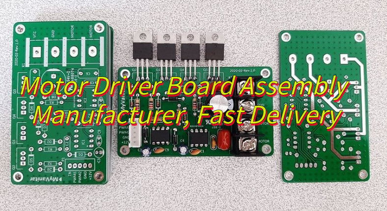
What is amotor driver board? Let’s discover meaning, components, function, application, usage guidelines, design guide and production process for motor driver board.
Are you troubled with these problems?
Slow motor response; need millisecond-level precise control?
Multi-axis signal interference; require stable communication?
Diverse customization needs; standard solutions hard to adapt, need rapid adjustment?
As a motor driver board assembly manufacturer, EBest Circuit (Best Technology) can provide service and solutions:
A motor driver boardis a core hardware module that bridges controllers and motors, converting low-power control signals (e.g., PWM, digital commands) into the precise current and voltage required to regulate motor start/stop, speed, direction, and rotation.
It integrates power switching components (MOSFET/IGBT), current sensors, and protection circuits to support DC, stepper, brushless, and servo motors. motor driver board’s features include overcurrent/overtemperature protection, EMI-resistant design, real-time feedback control, and high-efficiency energy conversion, ensuring stable operation for applications like robotics, automation, electric vehicles, and smart appliances.
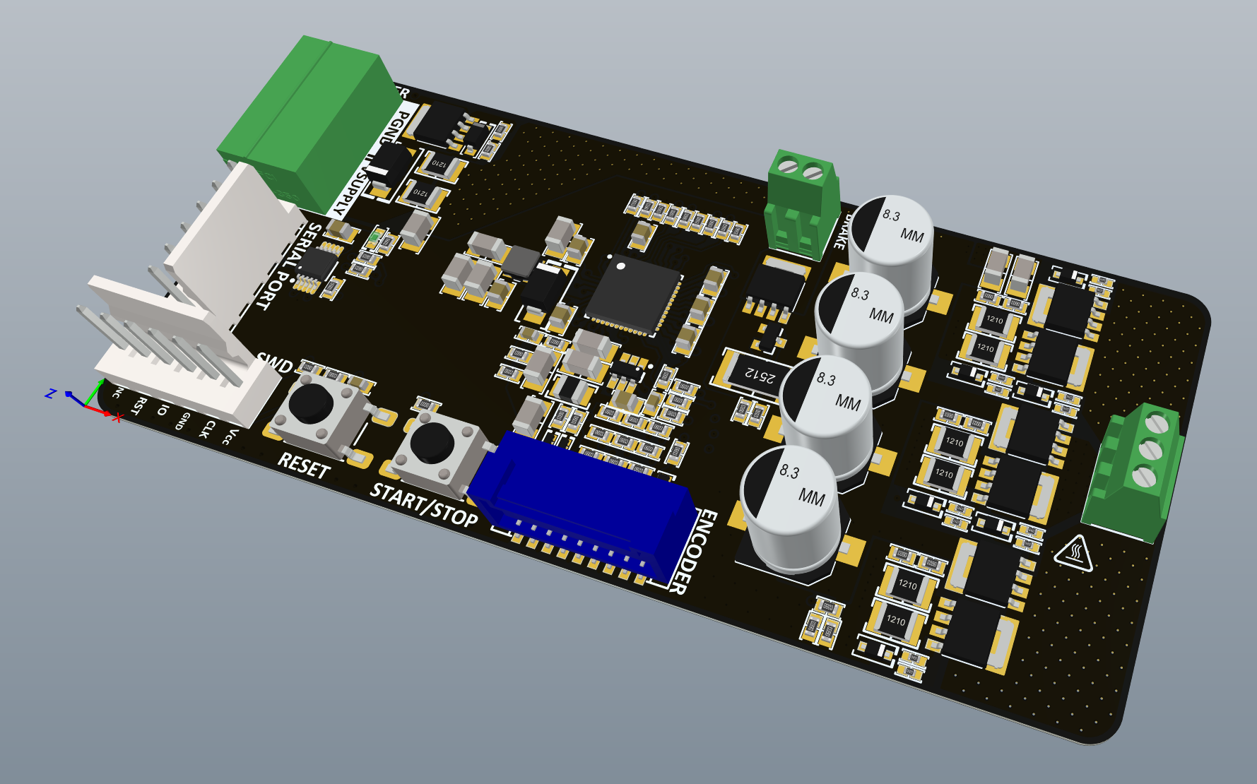
What Are the Components of a Motor Driver PCB?
Components of motor driver PCB:
Power Switches (e.g., MOSFETs): Convert low-voltage signals to high-current output, controlling motor start/stop and rotation direction.
H-Bridge Circuit: Enables bidirectional current flow via four coordinated switches, supporting forward/reverse rotation and braking.
Power Management: Stabilizes power via voltage regulators/filters, reduces EMI with layered design, and supports wide voltage/high current.
Control Circuit (MCU/Driver IC): Generates control signals, executes algorithms (e.g., PID), diagnoses faults, and isolates power/control domains.
Protection Modules: Safeguards against overcurrent, overvoltage, undervoltage, and overtemperature using sensors/TVS diodes.
Signal Processing: Hall sensors capture position/speed, processed via filtering/amplification; shunt resistors enable precise current control.
Interface & Communication: Supports protocols (CAN/SPI), uses shielded/differential pairs with ferrite beads for noise immunity, and includes debug interfaces.
Filtering & Energy Storage: Capacitors/inductors filter power ripple; RC networks reduce signal noise for accuracy.
Logic & Isolation: Optocouplers/digital isolators separate high/low-voltage domains, ensuring signal integrity and timing accuracy.
What Is the Use of a Motor Driver Board?
Functions of motor driver board:
Signal Conversion & Bridging: Serves as the core interface between controller and motor, converting low-power control signals into high current/voltage for precise driving.
Motion Control: Precisely regulates motor start/stop, speed, direction, and rotation angle, supporting forward/reverse rotation and braking modes.
Multi-Motor Compatibility: Compatible with DC, stepper, brushless, and servo motors to meet diverse application requirements.
Safety Protection: Integrates overcurrent, overvoltage, undervoltage, and overtemperature protection circuits/sensors to monitor and block abnormalities, preventing equipment damage.
Closed-Loop Feedback: Collects motor position/speed signals via Hall sensors/encoders, dynamically adjusts using algorithms (PID/FOC) to enhance control accuracy.
EMC Optimization: Uses layered PCB design, filtering circuits, and shielding to reduce EMI, ensuring stable signal transmission and system immunity.
What Are Applications of Motor Driver Circuit Board?
Applications of motor driver circuit board:
Electric wheelchair (including eye-controlled/smart wheelchair).
Robotic arm, CNC machine tool, engraving machine, 3D printer, material handling robot.
Electric car, electric scooter, drone, model aircraft, electric bicycle.
Robotic vacuum cleaner, smart home appliances, smart wristband.
Electric bed, electric height-adjustable desk, accessible elevator.
How to Use a Motor Driver Board?
1. Standardized Hardware Connection
Power connection: Use a power supply matching the motor’s rated voltage (e.g., 24V motor with 24V±10% regulated supply), connect with red-positive/black-negative standard wiring, secure with alligator clips or screw terminals.
Motor wiring: DC motor—positive to A+, negative to A-; stepper motor—phase wires in order to A-B-C-D terminals; brushless motor—connect three-phase power wires and Hall sensor signals with consistent phase.
Control signal wiring: Use physical switches/rotary potentiometers for control, e.g., rotate potentiometer clockwise to increase PWM duty cycle (accelerate motor), toggle switch to change DIR pin state (up for forward, down for reverse).
2. Manual Signal Calibration
Speed adjustment: Adjust PWM duty cycle via driver board’s built-in potentiometer (0-100% scale), each 10% rotation corresponds to stepped speed change (e.g., 20% for low-speed cruise, 80% for high-speed mode).
Direction control: Use DPDT switch for DIR pin, observe motor rotation change to confirm clear forward/reverse/stop states.
Braking: Activate BRAKE by pressing emergency stop button to short motor phases, generate reverse magnetic field for rapid braking, verify stopping time <2 seconds with tachometer.
3. Power & Protection Setup
Voltage monitoring: Use analog multimeter to check input voltage (±5% fluctuation limit), adjust voltage regulator or add filter capacitors if out of range.
Overcurrent protection: Adjust current limit via driver board’s trim pot (e.g., 5A to 10A), test with load simulator to verify protection triggers motor shutdown without burning smell.
Heat management: Apply thermal paste to heatsink, install aluminum bracket, monitor key components (e.g., MOSFET ≤80°C) with infrared thermometer, activate auxiliary fan for high temperatures.
4. Function Verification & Debugging
Basic test: Cycle “forward-reverse-brake” to check response time (≤0.5s), monitor current with clamp meter to ensure within rated range.
Closed-loop test: Connect encoder feedback, rotate motor shaft manually to check pulse proportionality, adjust PID knobs (e.g., increase P for faster response, decrease I for steady-state error) for speed control.
Troubleshooting: If motor jitters, check wiring errors or EMI; if overheating, check cooling or overload, reduce power output if necessary.
5. Safety & Maintenance
Pre-operation check: Inspect all connections before power-up, test insulation resistance (≥20MΩ) with megohmmeter, wear insulated gloves when handling rotating parts.
Emergency handling: Install independent emergency stop button in power circuit, press immediately for abnormalities; keep fire extinguisher nearby for electrical fires.
Regular maintenance: Clean dust quarterly, inspect capacitors for bulging/resistors for discoloration under magnifier, replace aged components; conduct full-function test semi-annually to meet factory standards.
How to Design a Power Wheelchair Motor Driver Board?
1. Core Circuit Module Design Parameters
Driver Circuit
Parameters: Use IR2104 isolated driver chip (gate voltage 10-20V, built-in dead time), matched with Hall sensors for current closed-loop control. Digital ground and power ground connected at a single point; sensitive signal lines filtered with ferrite beads.
Safety and Reliability Enhancements
Parameters: Redundant dual-channel input for critical control signals (e.g., PWM speed control), hardware watchdog circuit with ≤100ms response time. Temperature sensors and voltage monitoring circuits for real-time fault feedback.
2. Design Constraints
Physical Dimensions and Weight: PCB max dimensions must fit the whole vehicle (e.g., 1150x700x950mm), net weight ≤44Kg, payload ≥120Kg; trace spacing ≥10mil to prevent high-voltage breakdown.
Electrical Performance: Overcurrent protection threshold at 1.5x rated current; overtemperature protection using LM35 sensors (-40°C~150°C calibration); stall protection within 10 seconds. EMC compliant with ISO 7176-21, resistance to 26MHz-2.7GHz RF interference (≥20V/m), ESD tolerance ±8kV contact/±15kV air discharge with speed fluctuation ≤20% within 2 seconds.
Safety Standards: Must pass IEC 60601-1-2 medical EMC certification, CE certification, ISO13485:2003 quality certification, and CCC certification. Batteries/controllers/motors must individually pass GB/T 18029.21 testing.
3. PCB Layout and Routing Parameters
Layer Strategy: 4-layer PCB structure, top layer for power traces (copper thickness ≥2oz), bottom layer for control signals (50Ω impedance matching), inner layers for GND and power planes (copper coverage ≥30%).
Thermal Design: Copper foil heat dissipation under power devices, thermal vias in critical areas (thermal resistance ≤7.7°C/W); reserved mounting holes for heat sinks with thermal silicone application.
4. EMC Design Parameters
Filter Circuits: π-type filter at power input (100μH common-mode inductor + 1μF X-capacitor + 100nF Y-capacitor) to suppress conducted emissions (≤47dBμV/3m). Digital and analog grounds isolated via ferrite beads.
Shielding Measures: Metal shielding for control chip areas; critical signal traces routed away from high-frequency interference sources (e.g., wireless modules). Speed deviation ≤10°, steering deviation ≤10° when wireless devices (e.g., phones) are nearby.
5. Prototyping and Testing Parameters
Simulation Verification: SPICE tool for circuit-level simulation to validate power loop stability (loop bandwidth ≥1kHz) and control logic correctness.
Thermal Imaging: Infrared thermography to detect power device temperature rise (≤85°C) for thermal design optimization.
Long-Term Reliability: ≥1000-hour continuous aging test, vibration test per ISO 7176-13, thermal cycling test (-40°C~85°C, 500 cycles). Compliance with IPC-A-610 manufacturability standards and IPC-J-STD-020 soldering standards.
6. Documentation and DFM Parameters
BOM and Assembly: Detailed BOM with component models, parameters, capacitor values), and supplier info. Clear polarity, pad dimensions (e.g., QFN package soldering requirements). 3D models and assembly drawings with critical dimension tolerances (±0.1mm).
Certification Requirements: Mandatory compliance with IEC 60601-1-2, CE, ISO13485:2003, and CCC standards.
7. Design Considerations
Routing and Noise: Trace width ≥20mil to reduce parasitic inductance; Kelvin connections to eliminate ground bounce noise; driver signal traces ≤5cm to avoid signal reflection.
Mechanical and Environmental Protection: Stress relief slots at PCB edges to prevent solder joint fractures from vibration; moisture-resistant coating or potting (IP54 rating).
Manufacturability: Clear assembly guidelines for SMT processes, validated soldering temperature profiles, and compliance with IPC standards for component placement and inspection.
How to Assemble a Mobility Scotter Motor Driver Circuit Board?
Steps to Assemble a Mobility Scooter Motor Driver Board:
1. Component Preparation & Inspection
Verify component quantities and specifications (e.g., MOSFETs, driver ICs, capacitors) against BOM. Pre-tin power device leads and clean PCB pads if oxidized.
2. SMT Component Soldering
Use reflow soldering with temperature profile: 150°C preheat (60s), 180°C/s ramp to 220°C, 240°C reflow (40s), and natural cooling. Inspect solder joints for voids/bridging via microscope; X-ray BGA packages if applicable.
3. Through-Hole Component Installation
Solder through-hole parts (e.g., electrolytic capacitors, terminals) in height order (low to high), ensuring correct polarity for polarized components. Apply thermal grease between MOSFETs and heat sinks.
4. Electrical Verification
Perform static tests: check MOSFET GS/GD impedance, input-to-ground resistance, and signal line integrity.
Conduct dynamic tests: power up gradually, monitor LEDs/MCU status, and validate PWM signal fidelity with an oscilloscope.
5. Functional Module Testing
Configure driver IC parameters (e.g., dead time, current thresholds) via SPI/I2C. Calibrate Hall sensor alignment and test motor startup/stop sequences.
6. Protection Feature Validation
Simulate overcurrent via shunt resistor shorts; verify protection triggers (e.g., PWM disable, alarm LED). Test overtemperature response with localized heating.
7. System Integration & Optimization
Test wireless communication (e.g., Bluetooth) for real-time data exchange. Conduct environmental tests (high temperature, humidity, vibration) and EMC compliance checks.
Perform long-term aging tests and real-world road trials to confirm reliability and safety.
Why Choose EBest Circuit (Best Technology) as Motor Driver Board Assembly Manufacturer?
19-year PCBA expertise: 19 years of deep experience in motor driver board field with over 500 mature solutions, ensuring high technical maturity, reducing trial-and-error costs, and shortening development cycle by 30%+.
Strict quality control: From IQC incoming inspection to OQC final check, 6-step 100% functional testing, achieving ≥99.2% first-pass yield and ≤0.8% failure rate, ensuring equipment long-term stability.
Free DFM analysis: Design for Manufacturability evaluation identifying 20+ potential process risks, optimizing design in advance, cutting rework costs by 50%.
Stable supply chain: Strategic cooperation with 10+ core component suppliers, <7-day inventory turnover, ensuring zero material interruption and fast response to urgent orders.
One-stop service: Full-process coverage from PCB design to SMT assembly, functional testing, and packaging delivery, ensuring 100% on-time delivery and controlled project schedules.
48-hour rapid prototyping: Conventional motor driver boards prototyped within 48 hours, accelerating product validation and meeting agile development needs for robotics/industrial equipment.
Professional engineering support: 10+ senior engineers providing 7×12h technical response, resolving debugging issues within 24 hours, and boosting parameter configuration efficiency by 60%.
Environmental compliance: ISO 14001 and RoHS certified, meeting EU/North American environmental standards, ensuring smooth export and enhancing brand image.
Customized solutions: Support for power density optimization, EMC shielding design, etc., precisely matching product performance to application scenarios for differentiated competitiveness.
Welcome to contact us if you have any inquiry for motor driver board: sales@bestpcbs.com.
Looking for reliable PCB assembly services? This guide covers its benefits, applications, recommended assembly service supplier and how to get a quote to ensure quality and efficiency for your projects.
Are you worried about these issues?
How to handle PCB assembly delivery delays?
How to address hidden cost escalation in batch production?
How to resolve post-sale complaints caused by supplier quality fluctuations?
As a PCB assembly manufacturer, EBest Circuit (Best Technology) can provide service and solutions:
Advanced Production Scheduling System enables 48-hour rapid prototyping and 7-day mass production delivery to resolve delivery delay issues.
Modular design + bulk procurement reduces BOM costs by 15%, while automated production lines cut 30% labor overhead.
PCB Assembly Services refer to the professional manufacturing process of mounting electronic components onto printed circuit boards (PCBs) using surface-mount technology (SMT) or through-hole technology (THT), transforming bare boards into functional modules or semi-finished products. Typically outsourced by OEMs or designers, these services require design documents such as Gerber files and BOM lists. They cater to various production scales, from prototyping to mass production, and are widely used in industries like consumer electronics, automotive, and industrial equipment.
Compliant with ISO/IATF standards, simplifying certification for medical, automotive, and other demanding applications.
Scalable Production Flexibility
Seamless transition from small-batch prototyping (50+ units) to mass production, adapting to product lifecycle needs.
Fast response to urgent orders through capacity allocation, ensuring critical project deadlines.
What Problems Can PCB Assembly Services Solve?
PCB assembly servicesaddress several challenges in electronic manufacturing, including:
Design Implementation Barriers: Overcome physical realization challenges like high-density routing (e.g., 0.2mm BGA pitch) and irregular component layouts through professional CAM engineering.
High Prototyping Costs for Small Batches: Flexible low-minimum-order solutions (from 50 units) eliminate high tooling costs and MOQ barriers during validation.
Special Process Requirements: Enable advanced techniques: blind/buried vias, heavy copper (6oz+), ceramic substrates – surpassing lab fabrication limits.
19 Years of PCBA Expertise: Specialized in PCB assembly for 19 years, handling complex designs from prototypes to mass production with 99.8% yield stability.
Turnkey Solutions: Full-chain solutions from PCB inspection, component sourcing, SMT/DIP assembly, testing to packaging, submit designs, receive ready-to-market PCBAs.
Yamaha High-Speed Equipment: Equipped with Japanese Yamaha SMT lines for 01005-size components and 0.3mm BGA pitch precision, meeting miniaturization demands.
Four Parallel Production Lines: Flexible scheduling for rapid prototyping (48h) and scalable volume production, accelerating time-to-market.
Real-Time Traceability: MES-driven digital tracking for 100% process visibility—monitor progress, test reports, and quality data remotely.
Certified Quality Control: ISO 9001/IPC-A-610 compliant, with AOI/X-ray inspections ensuring zero defects and EU/US market readiness.
Bilingual Engineering Support: Direct technical communication with overseas engineers to minimize design-assembly gaps and rework risks.
24-Hour Rapid Prototyping: Quick-turn prototyping for design iteration, shortening development cycles.
Eco-Friendly Processes: Lead-free soldering and RoHS/REACH compliance for global environmental regulations.
Global Logistics Network: Partnered with DHL/UPS for secure, efficient worldwide delivery of assembled PCBs.
Our PCB Assembly Capabilities
Item
Capabilities
Placer Speed
13,200,000 chips/day
Bare Board Size
0.2 x 0.2 inches – 20 x 20 inches/ 22*47.5 inches
Minimum SMD Component
01005
Minimum BGA Pitch
0.25mm
Maximum Components
50*150mm
Assembly Type
SMT, THT, Mixed assembly
Component Package
Reels, Cut Tape, Tube, Tray, Loose Parts
Lead Time
1 – 5 days
How Are PCB Assembly Services Different from Other Solutions?
In-House Assembly
Features: Requires building a full production line with equipment like SMT machines, AOI inspection systems, and DIP plug-in tools, along with a dedicated engineering team.
Advantages: Full control over production processes, quality standards, and technical confidentiality, ideal for high-security products (e.g., military, medical devices) or large-scale stable mass production.
Challenges: High initial investment (equipment, factory, labor costs) and ongoing maintenance/upgrade expenses; small-batch production leads to significantly higher unit costs compared to outsourcing, with potential technology iteration delays.
Outsourced Assembly
Features: Entrusts professional PCBA manufacturers to handle partial or full assembly processes, leveraging their mature technologies, economies of scale, and supply chain resources.
Advantages: Reduces fixed asset investment and adapts flexibly to small-batch, multi-variety orders; enables quick access to advanced processes (e.g., HDI, micro-BGA packaging); lowers costs through centralized procurement by suppliers, particularly suitable for agile R&D needs of SMEs.
Challenges: Requires rigorous vetting of supplier qualifications (e.g., ISO certification, IPC standards) to avoid quality risks; coordination costs for logistics and communication may cause response delays.
Turnkey Solutions
Features: Offers end-to-end services covering BOM sourcing, PCB fabrication, component placement, functional testing, and logistics delivery. Clients only need to provide design files to receive complete products.
Advantages: Greatly simplifies client management processes and shortens project cycles (e.g., 48-hour rapid prototyping); achieves full traceability via digital systems (e.g., DFM verification, transparent progress dashboards) to minimize human errors; reduces BOM costs by 15%+ through centralized procurement and supply chain optimization, addressing “minimum order quantity” and “hidden cost” issues for small batches.
Application Scenarios: Ideal for rapid prototyping in R&D phases, small-batch trial production, multi-variety agile manufacturing, and innovative projects requiring strict cost control and fast time-to-market.
How to Get a Quote for PCB Assembly Service?
To get a quote for PCB assembly service, you need to submit the following materials list:
Gerber Files: Standard format for PCB design data.
Bill of Materials (BOM): Complete list of components with part numbers, quantities, and reference designators.
Pick-and-Place File: Machine-readable file for component placement (e.g., .csv, .txt).
Assembly Drawings: Visual guides for component placement and orientation.
Special Instruction: Any unique requirements (e.g., conformal coating, testing protocols).
Quantity & Lead Time: Estimated order volume and required turnaround time.
Contact Us Today
If you have any questions about our PCB assembly services or would like to request a quote, feel free to contact us: sales@bestpcbs.com. We are committed to providing the best quality, pricing, and services to meet your PCB assembly needs.
How to remove copper from PCB? This guide compares chemical, mechanical, and eco-friendly removal techniques, plus safety tips to help you choose wisely.
Are you worried about these issues?
Is 5G signal distortion plaguing your circuit?
Is PCB cost overrun eating profits?
Is impedance mismatch ruining RF designs?
As a PCB manufacturer, EBest Circuit (Best Technology) can provide service and solution:
High-Frequency Copper Removal: Laser-etch to eliminate parasitics, boost 5G signal speed by 15%.
Cost Efficiency Surgery: AI-driven copper trimming cuts waste, slashes unit cost by 8%.
Impedance Control Mastery: Micron-level precision + real-time testing ensures ±5Ω tolerance, passes ISO 9001 first try.
Welcome to contact us if you have any request for PCB design and manufacturer: sales@bestpcbs.com.
Surface Cleaning: Clean the copper-clad laminate using fine sandpaper (400-600 grit) or isopropyl alcohol/ultrasonic cleaning to eliminate oil, oxides, and contaminants. Mechanical cleaning involves scrubbing with a brush and mild detergent, followed by rinsing with deionized water. Ensure complete drying to prevent etching unevenness from residual moisture.
Pattern Transfer: Employ photolithography or thermal transfer techniques. For photolithography, apply photoresist (dry film or liquid) and expose it under UV light through a mask film. Develop with a 0.8-1.2% sodium carbonate solution to remove unexposed resist. For thermal transfer, use laser-printed mirrored patterns on transfer paper, heat-press at 150-180°C onto the board, and dissolve the paper in warm water.
Resist Curing: Post-exposure baking at 80-100°C for 10-15 minutes or UV curing (365nm, 50-100mJ/cm²) ensures resist adhesion and chemical resistance.
2. Etchant Selection and Preparation
Acidic Etchant: A mixture of copper chloride (CuCl₂), hydrochloric acid (HCl), and hydrogen peroxide (H₂O₂). The reaction is Cu + H₂O₂ + 2HCl → CuCl₂ + 2H₂O. Optimal conditions: 1-1.5M Cu²⁺, pH 1-2. Add stabilizers (e.g., urea) to prevent H₂O₂ decomposition.
Alkaline Etchant: Ammoniacal copper chloride system (CuCl₂ + NH₃ + NH₄Cl), forming [Cu(NH₃)₄]²⁺ complexes. Maintain pH 8.0-8.8, temperature 45-55°C, and Cu²⁺ concentration 18-22 oz/gallon (7.5-8.5 g/L). Add NH₄Cl at 150-200 g/L for enhanced regeneration.
Preparation Protocol: Use deionized water for mixing. Adjust HCl to 2-3M for acidic etchant; maintain NH₃:NH₄Cl ratio at 3:1 for alkaline etchant. Stir continuously to avoid precipitation.
3. Etching Operation and Control
Method Selection: Spray etching (preferred for uniformity), bubble etching, or immersion etching. Spray systems operate at 0.2-0.4 MPa; immersion tanks require 200-300 rpm stirring.
Time: Adjust based on copper thickness (e.g., 18μm Cu requires 2-5 min). Thick copper (>35μm) may need multiple passes.
Side Etch Control: Use additives (e.g., benzotriazole) to maintain an etch factor ≥3. Reduce spray pressure for fine lines (<75μm) to minimize undercut.
Monitoring: Use inline sensors to track Cu²⁺ concentration, pH, and temperature. Automatic systems replenish etchant via titration or density control.
4. Post-Processing and Quality Inspection
Cleaning and Neutralization: Rinse with deionized water for 2-3 minutes. Neutralize acidic residues with 5-10% Na₂CO₃; acid-wash alkaline residues with 1-2% HCl.
Resist Removal: Dissolve dry film in 3-5% NaOH at 50°C; liquid resist requires acetone or commercial stripper. Gently scrub to avoid damaging copper traces.
Quality Checks:
Microscopic Inspection: Use 50-200X optical microscopy to verify line integrity, width tolerance (±10μm), and absence of pinholes.
Electrical Testing: Perform continuity and isolation tests with a multimeter or flying probe tester.
Repair: Fill gaps with conductive ink or re-plate copper for broken traces.
5. Safety and Environmental Protection
Personal Protection: Wear nitrile gloves, chemical goggles, acid-resistant aprons, and respirators in ventilated fume hoods. Ensure access to emergency eyewash and shower stations.
Waste Management: Collect spent etchant in labeled containers. Acidic waste precipitates Cu(OH)₂ with lime; alkaline waste recovers Cu via electrolysis. Dispose through licensed facilities adhering to EPA/ROHS standards.
Equipment Maintenance: Clean etching tanks weekly with 5% HNO₃ to remove residues. Inspect pumps, nozzles, and heaters monthly to prevent leaks or clogging.
What Chemical Solutions Dissolve Copper from PCBs?
Chemical Solutions for Dissolving Copper from PCBs
Acidic Copper Chloride Etchant
Composition & Principle: Primarily composed of copper chloride (CuCl₂), hydrochloric acid (HCl), and hydrogen peroxide (H₂O₂). The reaction is Cu + H₂O₂ + 2HCl → CuCl₂ + 2H₂O, forming soluble complexes.
Application Scenarios: Suitable for fine-line PCBs (e.g., HDI boards) due to fast and uniform etching rates.
Operation Points: Maintain Cu²⁺ concentration at 1–1.5 M, pH 1–2, and temperature ≤60°C to prevent H₂O₂ decomposition. Regularly monitor ORP (500–600 mV) and specific gravity (1.3 ± 0.03) to avoid excessive side etching.
Alkaline Copper Chloride Etchant
Composition & Principle: Contains copper chloride, ammonia (NH₃), and ammonium chloride (NH₄Cl), forming [Cu(NH₃)₄]²⁺ complexes. Slower etching but high precision.
Application Scenarios: Ideal for multilayer boards, flexible PCBs (FPCs), and scenarios requiring high etch factor (≥3).
Operation Points: Maintain pH 8.0–8.8, temperature 45–55°C, and Cu²⁺ concentration 18–22 oz/gallon (~7.5–8.5 g/L). Add NH₄Cl (150–200 g/L) to enhance regeneration and prevent ammonia volatilization.
Sodium Persulfate Etchant
Composition & Principle: Sodium persulfate (Na₂S₂O₈) reacts with acid (e.g., sulfuric acid) to produce CuSO₄ and Na₂SO₄. Etching rate adjustable via temperature (40–60°C) and pH (2–5).
Application Scenarios: Small-batch production, flexible boards, and inner-layer etching for HDI boards, with environmental advantages (easy copper recovery from waste liquid).
Operation Points: Use activators (e.g., iron powder) to improve efficiency and reduce side etching. Neutralize waste liquid for copper precipitation or recovery via electrolysis.
Ferric Chloride Etchant
Composition & Principle: Ferric chloride (FeCl₃) reacts with copper via redox reaction, generating Cu²⁺ and Fe²⁺. Suitable for screen-printed PCBs and liquid photoresists.
Application Scenarios: Low-cost, widely available, but prone to side etching. Not recommended for nickel/tin-resistant layers.
Operation Points: Regularly replenish the solution. Neutralize waste liquid with lime to precipitate Cu(OH)₂ for disposal.
Fluoroboric Acid Etchant
Composition & Principle: Mixture of fluoroboric acid (HBF₄) and nitric acid, dissolving copper to form fluoride complexes. Used for special alloy etching (e.g., magnesium alloy demolding, IC wafer trenches).
Operation Points: Wear acid-resistant protective gear. Neutralize waste liquid with soda ash to precipitate calcium fluoride, meeting environmental standards.
How Does Mechanical Grinding Remove Copper from PCB Effectively?
1. Pre-Surface Treatment and Assessment
Cleaning and Inspection: Remove surface oils, oxides, and residues using anhydrous ethanol or ultrasonic cleaning to ensure full contact between abrasive media and copper layers. Measure copper thickness (typically 18-70μm), uniformity, and substrate durability (e.g., FR4, polyimide) via optical microscopy or XRF spectroscopy to prevent substrate damage from over-grinding.
Area Marking: Protect critical circuit areas (e.g., pads, traces) with high-temperature tape or solder mask to avoid accidental damage during grinding.
2. Tool and Media Selection
Manual Grinding: Use silicon carbide/alumina sandpaper (80-1200 grit) with handheld blocks or rotary tools (e.g., Dremel) for localized, fine-area grinding.
Automated Grinding: Employ planar grinders, belt sanders, or CNC machines equipped with diamond wheels, ceramic discs, or nylon brushes for large-scale, batch processing. Adjust belt grit (P120-P400) and pressure (0.2-0.5MPa) to control efficiency.
Sandblasting: Utilize compressed air-driven alumina/glass bead blasting with adjustable pressure (0.4-0.8MPa), nozzle distance (10-30cm), and angle (45°-90°) for uniform copper removal on complex surfaces or multi-layer board edges.
3. Precise Parameter Control
Pressure and Speed: Optimize grinding pressure (0.1-0.3MPa) based on copper thickness and substrate hardness to avoid deformation or delamination. Balance speed (e.g., belt linear speed 15-30m/s) with surface quality, excessive speed causes thermal damage, while low speed reduces efficiency.
Cooling and Lubrication: Continuously apply coolant (deionized water or specialized grinding fluid) to reduce friction heat, minimize dust, and extend media life.
Multi-Stage Strategy: For thick copper (>35μm), adopt “coarse-medium-fine” multi-step grinding with progressively finer grits to prevent uneven substrate exposure or burrs.
4. Process Monitoring and Quality Inspection
Real-Time Monitoring: Use inline thickness gauges or laser sensors to track copper removal thickness and uniformity. Inspect surfaces visually or via magnifiers for residual copper, scratches, or substrate damage.
Post-Process Inspection: Clean surfaces with compressed air and ethanol, then verify roughness (Ra ≤1.6μm), copper residue, and substrate integrity using optical/electron microscopy (50-200X) per IPC-A-600 standards.
Electrical Testing: Perform continuity and isolation tests (e.g., flying probe testing) to confirm circuit functionality and rule out shorts/opens caused by grinding.
5. Environmental and Safety Measures
Dust Control: Operate within negative-pressure dust chambers or enclosed systems with HEPA filtration to capture copper particles, preventing environmental contamination and operator exposure.
Personal Protection: Wear dust masks, safety goggles, earplugs, cut-resistant gloves, and anti-static clothing to shield against debris, noise, and electrostatic discharge.
Waste Recovery: Recover copper powder via magnetic separation or chemical precipitation; treat waste fluids through neutralization/sedimentation to meet discharge standards (e.g., GB 8978-1996).
Can Ultrasonic Cleaning Remove Copper from PCB without Damaging Substrates?
No, ultrasonic cleaning alone cannot remove copper from PCBs without damaging substrates. Ultrasonic cleaning primarily utilizes cavitation bubbles to dislodge surface contaminants like oils, oxides, or residues, but it does not chemically or mechanically etch copper. Effective copper removal requires dedicated methods such as chemical etching (e.g., acidic/alkaline solutions) or mechanical grinding, which directly dissolve or abrade the copper layer while substrate protection depends on precise parameter control (e.g., temperature, pressure, time) and protective coatings.
Are There Eco-Friendly Alternatives to Remove Copper from PCB?
Yes, there are eco-friendly alternatives to remove copper from PCB, with several technologies already achieving industrial-scale application. Below is a detailed analysis with enhanced technical specifics:
1. Mechanical Stripping (Physical Eco-Solution)
Technical Enhancement: Utilize precision tools like 80-120 grit sandpaper for coarse removal, followed by 2000-grit polishing for fine finishing. Laser ablation employs 355nm UV lasers at 5-10W power with 100-500mm/s scanning speeds, achieving ±5μm edge precision.
Eco-Advantage: Zero chemical waste generation; copper dust collected via HEPA filters can be smelted into 99.9% pure copper ingots.
Case Example: A prototyping lab reduced chemical waste by 85% using laser stripping for 0.5oz copper layers.
Process Innovation: Electrolytic recovery systems operate at 0.5-2A/dm² current density with pH control between 2-3. Pulse power supply technology reduces energy consumption by 30% compared to DC systems.
Recovery Efficiency: Copper ions precipitate as CuSO₄·5H₂O crystals, achieving 98% purity for direct reuse in PCB plating lines.
Industrial Application: A manufacturer recovered 15 tons of copper annually through closed-loop electrolysis, cutting raw material costs by 40%.
3. Bio-Etching (Cutting-Edge Biotechnology)
Microbial Action: Acidithiobacillus ferrooxidans bacteria oxidize copper at 30-35℃ in nutrient-rich solutions. Laboratory tests show complete dissolution of 20μm copper layers within 48 hours.
Byproduct Handling: Fermentation broth undergoes simple pH adjustment (to 7-8) before discharge, meeting municipal wastewater standards.
Scalability Challenge: Current pilot-scale systems process 100m² PCBs/day at $15/m² cost, 3x higher than chemical methods but decreasing with R&D advances.
4. Dry Etching Technologies (Waste Minimization)
Vacuum Etching: Patented flat-jet nozzles deliver etching solution at 20m/s velocity, reducing liquid usage by 30% while maintaining ±1μm uniformity for ≤30/30μm lines.
Plasma Etching: Inductively coupled plasma (ICP) systems use SF₆/O₂ mixtures to sputter copper at 50-100nm/min rates, ideal for ultra-thin flexible PCBs.
5. Eco-Friendly Etchant Formulations
Sodium Persulfate System: Enhanced with 0.5% sodium dodecyl sulfate for improved wetting, achieving 15% faster etching rates than conventional recipes. Wastewater treatment involves precipitation with 2g/L Na₂S, reducing copper to <0.5mg/L.
Citric Acid Blend: A 15% citric acid solution with 5% H₂O₂ provides biodegradable etching at 40℃, with ozone post-treatment degrading residual organics to CO₂/H₂O.
What PPE is Mandatory When Remove Copper from PCB with Acids?
Necessity: Acidic etching solutions are highly corrosive; direct contact can cause chemical burns or tissue necrosis.
Recommended Standard: Nitrile gloves compliant with EN374 standards, thickness ≥0.5mm, ensuring flexibility for dexterous operations. Inspect gloves for integrity before use; replace immediately if damaged.
Full-Face Protective Goggles (with Facial Shield)
Necessity: Splash hazards pose risks of permanent eye/facial injuries.
Recommended Standard: ANSI Z87.1-certified goggles with anti-splash coating, clear distortion-free vision. Optimize for models with integrated facial shields for 360° protection.
Acid-Resistant Raincoat/Chemical Apron
Necessity: Torso and lower limbs are high-risk areas for accidental acid splashes; regular clothing offers no protection.
Recommended Standard: PVC or neoprene material, covering knee-length with sealed seams. Choose knee-high designs to prevent entanglement during operations.
Dust Mask (for Powder Handling)
Necessity: Powdered reagents like ferric chloride generate inhalable dust, risking respiratory diseases with prolonged exposure.
Recommended Standard: N95/FFP2-certified masks with exhalation valves for reduced breathing resistance. Replace filters regularly to maintain efficiency.
Corrosion-Resistant Boots (Rubber Material)
Necessity: Acid penetration through footwear can cause severe foot burns.
Recommended Standard: Knee-high rubber boots with anti-slip soles, boot height ≥30cm. Must pass acid-resistance tests for prolonged use without leakage.
Emergency Eyewash/Shower Station
Necessity: Immediate rinsing is critical for acid exposure to skin/eyes; delays risk irreversible damage.
Installation Requirements: Eyewash flow ≥1.5L/min, full-body shower accessible within 10 seconds. Regularly inspect equipment functionality and water purity.0
FAQs of Copper from PCB Removal
Q1: How do differences in etchant corrosion to PCB substrates influence process selection? A1: Acidic etchants (e.g., copper chloride systems) exhibit lower corrosion to FR4 epoxy substrates, ideal for fine-pitch circuits. Alkaline ammonia-based etchants are gentler to polyimide flexible substrates but require ammonia volatilization control. Sodium persulfate systems, free of ammonia, suit odor-sensitive environments. Selection depends on substrate type, line precision, and environmental regulations.
Q2: How to adjust grinding parameters to prevent substrate delamination during mechanical removal? A2: For thick copper (>35μm), adopt multi-stage grinding: coarse (80-grit) → medium (240-grit) → fine (400-grit) with progressive grit reduction. Maintain low pressure (0.1-0.3MPa) and belt speed (15-30m/s) to avoid over-grinding. Real-time thickness monitoring ensures uniform removal.
Q3: How to ensure copper ion concentration meets discharge standards during waste liquid treatment? A3: Neutralize waste liquid to pH 6-9 (lime for acids, sulfuric acid for alkalis), then precipitate copper as CuS/Cu(OH)₂ using Na₂S/NaOH. Separate solids via filter press. Further purify filtrate via ion exchange/electrolysis to achieve Cu²⁺ <0.5mg/L, compliant with GB 8978-1996.
Q4: How to control undercut for line precision during acidic etching? A4: Maintain Cu²⁺ at 1-1.5M, pH 1-2, temperature ≤60°C. Monitor ORP (500-600mV) and specific gravity (1.3±0.03). For high precision, alkaline ammonia etchants form [Cu(NH₃)₄]²⁺ complexes to reduce undercut, requiring etching factor ≥3.
Q5: What environmental compliance factors should prioritize when selecting copper removal methods? A5: Evaluate waste treatment costs and copper recovery efficiency (e.g., >99.9% purity via electrolysis). Ensure facilities have negative-pressure dust control, HEPA filtration, and emergency showers. Comply with OSHA/local regulations for chemical exposure and wastewater COD (<100mg/L).
The copper busbar manufacturing process combines heavy-copper PCB techniques with precise metalwork. It begins with careful design to control current and heat. Pure copper sheets or bars are cut, cleaned, and prepared for bonding.
During lamination or bar insertion, the copper forms a solid low-resistance path inside the PCB stack. CNC drilling and routing create exact holes and outlines. Plating with tin, nickel, or silver protects the surface and improves soldering.
Finally, each board is tested for conductivity, flatness, and insulation strength. This streamlined process delivers reliable, high-current PCBs for demanding power-electronics applications.
EBest Circuit (Best Technology) has nearly 19+ years of experience in PCB manufacturing, offering a one-stop service for bus bar PCBs from layout design, diagram evaluation, prototyping and mass production to after-sales service. We are certified by ISO9001, ISO13485, IATF16949, and UL, ensuring high-quality PCBs with fast delivery. As experts in bus bar PCB manufacturing, custom bus bar PCBs are available according to your specific requirements.
What is copper busbar PCB?
Copper busbar PCB is a printed circuit board with thick copper layers or inserted copper bars that move high current. It is different from a normal PCB.
Traditional boards handle small to medium current. A bus bar PCB carries far more power while keeping temperature under control.
Engineers place a solid copper bar or heavy copper layer inside the PCB stack-up. Applications include renewable energy systems, electric vehicles, industrial drives, and telecom power units. These fields need a safe, low-loss path for energy.
What is the raw material of copper busbar?
The key ingredient is pure copper with a high conductivity grade. Most manufacturers use C1100 or equivalent electrolytic tough pitch copper.
This type of copper contains more than 99.9% purity. It resists oxidation and carries current with minimal loss.
For insulation, makers use FR-4, polyimide, or other high-temperature PCB substrates. Epoxy resins with strong bonding power hold the layers together.
Surface finishes such as nickel, tin, or silver plating protect the copper from corrosion. The choice depends on the end use.
BEST Technology sources these materials only from certified producers. Stable raw stock ensures each busbar meets strict electrical and mechanical requirements.
How to make a copper busbar?
The copper busbar manufacturing process blends PCB technology with precision metalwork. Here is a clear view of the main stages:
1. Design and Simulation
Engineers design the current path and thickness. They run thermal and electrical simulations.
2. Copper Cutting and Preparation
High-purity copper sheets or bars are cut to exact size. Any surface oxide is removed.
3. Lamination or Bar Insertion
Two common methods exist.
Heavy copper lamination adds extra copper layers during PCB pressing.
Bar insertion places a pre-machined copper bar inside the board.
Both create a strong, continuous conductor.
4. Drilling and Routing
Precise CNC drilling forms mounting holes and routing channels.
5. Plating and Surface Finish
Nickel, tin, or silver is plated on exposed copper. This guards against oxidation and improves solderability.
6. Solder Mask and Legend
A protective solder mask covers non-conductive areas. Markings identify polarity and connection points.
7. Testing and Inspection
Manufacturers test current capacity, insulation resistance, and thermal rise. Only boards that meet design specs move forward.
Each stage demands strict process control. High-power electronics cannot tolerate flaws. Experienced copper bus bar manufacturers BEST TECHNOLOGY use advanced equipment to keep every parameter consistent.
What matters most in Copper Bar Production for PCBs?
Several factors decide final quality:
Conductivity: Copper purity is critical.
Thickness: Adequate thickness handles the required amperage without excessive heat.
Flatness: Perfectly flat bars ensure tight contact with PCB layers and connectors.
Compact Design: High current moves through smaller space, reducing overall footprint.
High Reliability: Strong copper core resists fatigue and vibration.
Cost Efficiency: Fewer parallel traces and connectors lower assembly time.
These advantages matter in heavy-duty power electronics. Solar inverters, battery systems, and EV chargers need reliable high current flow every day.
Why should you use a bus bar PCB for power electronics?
Power electronics depend on efficient current distribution. A bus bar PCB cuts energy loss and enhances thermal performance.
Instead of routing multiple wide traces, designers integrate a single copper bus. This reduces connection points and lowers risk of loose joints.
The solid copper path also handles sudden current spikes. Equipment stays stable under load changes.
Maintenance becomes simpler. The board lasts longer with fewer hot spots and less stress on components.
What are the applications of Bus Bar PCB?
You will find bus bar PCBs across many industries:
Electric Vehicles: Battery management and drive inverters.
Renewable Energy: Solar power inverters and wind turbines.
Industrial Equipment: High-power motor controls and automation systems.
Telecom and Data Centers: Power distribution units for stable uptime.
Medical Devices: Imaging systems that demand steady high current.
In every case, heavy copper boards secure strong performance and safe operation.
Conclusion:
Copper busbar PCB offers unmatched power handling, heat control, and reliability. From pure copper raw materials to careful plating, every step of the copper busbar manufacturing process must meet strict standards.
EBest Circuit (Best Technology) Co., Ltd. is one of the trusted copper busbar manufacturers with factories in China and Vietnam. We deliver quick lead times, high precision, and competitive pricing. Our team provides a free first sample and 24-hour technical response.
For detailed specifications or a custom quote, reach out to sales@bestpcbs.com
As a LED MCPCB Manufacturer, We are proud to provide a wide variety of MCPCBs for the lighting world. With over 19 years of experience in designing and manufacturing MCPCBs, we take pride in being your one-stop supplier.
As a trusted supplier, we hold certifications including UL, ISO13485, ISO9001, IATF16949 and SGS, enabling us to meet the high standards of clients across Europe, America, Israel, India, and so on. Explore our services and let us help you fulfill your MCPCB needs.
Are you looking for LED MCPCB Manufacturer? Do you have any questions?
What types of MCPCBs do you mainly produce?
Do you support customized designs?
What is the typical delivery time? Do you offer expedited service?
What after-sales service and technical support do you provide?
As a MCPCB manufacturer with 19+ years of experience, BEST Technology can tell you:
Based on metal substrate type, we offer copper, copper-aluminum, aluminum, and steel substrates. Based on product structure, we offer thermal and electrical separation MCPCBs, rigid-flex MCPCBs, and single- and double-sided multilayer MCPCBs.
We offer one-stop customized solutions from design to production.
Standard delivery time is 5-10 business days; we also offer expedited service, and urgent boards can be shipped out within 24 hours!
Quality inspection and returns and exchanges are included. We also provide design-for-manufacturing (DFM) advice, technical consulting, and troubleshooting services.
What is MCPCB LED?
An MCPCB LED is a light-emitting diode mounted on a Metal Core Printed Circuit Board. Unlike a standard circuit board, an MCPCB uses a metal plate as the base. This metal core, usually aluminum or copper, moves heat away from the LEDs fast. Heat is the main reason LEDs fade or fail. A board that spreads heat keeps them bright and strong.
MCPCB LEDs appear in almost every modern lighting product. LED panels for offices, car headlights, medical lamps, and industrial floodlights all rely on this design. The solid metal base creates a powerful thermal path. That means longer life, steady color, and reliable brightness.
Which board is better for LEDs: MCPCB or standard FR-4?
FR-4 is a fiberglass and epoxy laminate. It works for many electronics. But LEDs run hot and need better heat transfer.
As a MCPCB led manufacturer, BEST Technology can tell you the advantages of MCPCB:
Metal base moves heat away quickly.
LEDs stay at a safe operating temperature.
Brightness and color remain stable for years.
FR-4 costs less for simple circuits. Yet for high-power LED lights, it can become a weak link. Over time heat builds up. That can reduce LED life and cause early dimming.
When a product demands long service and high brightness, MCPCB is the better choice. The small extra cost pays back through fewer failures and less maintenance.
What is a Metal Core PCB and why do LEDs need it?
A Metal Core PCB has a solid metal plate inside the board. Most often that plate is aluminum. Some high-performance designs use copper or a mix of alloys.
The structure is simple but powerful. A thin dielectric layer separates the copper circuit from the metal base. This dielectric must be thermally conductive yet electrically insulating.
LEDs convert electricity into light. That process produces heat. If heat stays near the LED chip, performance drops. Light output falls, and lifetime shortens.
The metal core solves this. Heat flows fast from the LED junction through the dielectric into the metal base. From there it moves to a heat sink or the surrounding air. This keeps the LED at an optimal temperature.
With a cooler junction, the LED can handle higher current and stay bright. This is why china mcpcb led board manufacturers focus on precise thermal design.
How does the LED PCB assembly process work for MCPCBs?
Building an LED MCPCB involves several careful steps. Professional led pcb assembly lines follow strict procedures:
Material Preparation: Aluminum or copper base plates are cleaned and coated with a thin dielectric.
Circuit Imaging and Etching: Copper foil is laminated and patterned. Chemical etching forms the circuit traces.
Solder Mask and Surface Finish: A heat-resistant solder mask protects the copper. ENIG or OSP finishes create strong solder joints.
Component Placement: High-speed pick-and-place machines set LEDs and other parts accurately.
Reflow Soldering: Boards pass through a controlled oven. Solder paste melts and bonds components to the pads.
Inspection and Testing: Automated optical inspection checks for alignment and solder quality. Electrical and thermal tests confirm performance.
BEST Technology, a top factory in China, completes these steps using advanced SMT production lines. They deliver high volumes without losing precision. This is key for reliable LED products used in street lights, automotive lamps, and large LED panels.
How does a MCPCB led manufacturer solve LED thermal problems?
LED heat management is critical. BEST Technology, an Skilled led mcpcb manufacturers china, addresses this issue in several ways:
Metal Core Design: Aluminum or copper spreads heat evenly.
High-Conductivity Dielectric: Special materials reduce thermal resistance.
Optimized Pad Layout: Careful spacing prevents hot spots.
Precise Thickness Control: Balances insulation with thermal transfer.
Quality Solder and Mounting: Good solder increases heat flow from the LED to the metal base.
Many manufacturers run thermal simulations during design. We predict how the board will behave in real conditions. This ensures LED panels stay cool even under heavy load.
Better heat management means brighter light and longer life. As a customer, you get a highly efficient product with lower maintenance requirements.
What materials are used in high-performance Metal Core PCBs?
The choice of materials defines the performance of a Metal Core PCB. Reliable mcpcb led manufacturer facilities use:
Base Metal: Aluminum for general use. Copper when very high conductivity is needed.
Dielectric Layer: Thin, thermally conductive polymer. Often 1 to 2 W/m·K for standard boards and up to 8 W/m·K for premium boards.
Copper Circuit Layer: Usually 1 to 3 ounces per square foot for strong current carrying.
Solder Mask: Heat-resistant and protective.
Surface Finish: ENIG, OSP, or Immersion Silver for excellent soldering and corrosion resistance.
Some designs add graphite or special composites to improve heat spreading. These materials keep boards stable even in harsh outdoor or automotive conditions.
Which tests prove an LED MCPCB is safe and durable?
Thermal Cycling: Rapid hot and cold cycles confirm the board can handle temperature changes.
Hi-Pot Testing: Ensures the dielectric insulates properly between copper and metal base.
Vibration and Shock Testing: Checks stability for automotive or industrial uses.
Solderability Testing: Verifies pads accept solder without defects.
Burn-In: LEDs run at high current for hours to reveal hidden issues.
These tests ensure product performance in real-world environments. You can trust this circuit board for applications in LED displays, medical lamps, and automotive lighting.
What certifications must LED MCPCB manufacturers in China have?
Quality and safety certifications show a manufacturer meets international standards. Important approvals include:
ISO 9001:2015: Quality management for consistent production.
UL Certification: Safety standard for PCB materials.
RoHS and REACH: Proof that materials meet environmental rules.
ISO 14001: Environmental management for clean manufacturing.
IATF 16949: Required for automotive LED applications.
BEST Technology holds relevant quality certifications, which proves our ability to provide high-quality products. These certifications are a guarantee of product excellence, ensuring that customers and partners receive good quality assurance.
Conclusion:
LED lighting needs strong thermal control. Metal Core PCBs give that control through fast heat transfer and stable performance. Compared with FR-4, MCPCB boards keep LEDs brighter and longer-lasting.
For dependable LED MCPCBs, EBest Circuit (Best Technology) Co., Ltd. offers proven quality and responsive service. Contact sales@bestpcbs.com for samples or custom quotes.