What are vias in PCB design?
Via hole is one of the important components of multi-layer PCB, and the cost of drilling usually accounts for 30% to 40% of the PCB board cost. Simply put, every hole on the PCB can be called a pass hole. From the function point of view, the hole can be divided into two categories: one is used as an electrical connection between the layers. The second is used as the fixing or positioning of the device.
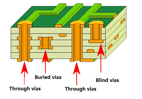
From a manufacturing process perspective, vias can be divided into three types: blind vias, buried vias, and through vias:
- Blind vias: These connect the surface layer to an internal layer, without going through the entire board. Their depth is typically related to the hole diameter.
- Buried vias: Located inside the PCB, they don’t reach the surface.
- Through vias: These pass through the entire board and are the most common due to their lower manufacturing cost and simpler process.
How to make PCB vias?
Typically, PCB vias are produced following the IPC-2 standard, where the copper thickness in the hole is around 0.8 mil to 1 mil. However, in practice, the copper plating might not be uniform, and the thinnest part could be as narrow as 0.7 mil, affecting the current-carrying capacity.
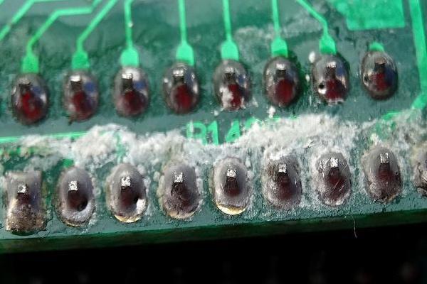
Generally, the conventional PCB board is produced according to IPC-2 standard, where the copper thickness in the hole is around 0.8 mil to 1 mil (you can check the specific content of the IPC-2 standard). The hole that we think is produced during production is this ideal situation (as shown below), the size of the hole is regular, and the thickness of the hole copper is very symmetrical:
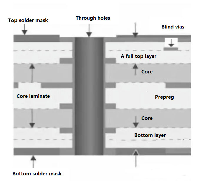
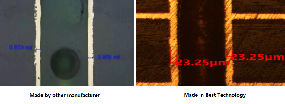
However, in practice, the copper plating might not be uniform. As you can see, the copper plating thickness of the perforated wall of the PCB produced in general may be wide up and down, and narrow in the middle, so the narrowest limit may be 0.7mil. It can be imagined that if the current carrying situation is evaluated, it should be calculated according to the smallest and smallest cross-sectional area, but the smallest cross-sectional area is deviated from the actual design value. But actually, a good PCB manufacturer can help to save much time and money for you, you can see the via holes cross-sectional made by EBest Circuit (Best Technology) and others.
What Is the Current Carrying Capacity of a Via?
The current-carrying capacity of a via refers to the maximum current it can safely handle. In PCB design, vias are essential components that connect traces between layers, and their size and shape directly impact how much current they can carry. Factors affecting current capacity include via diameter, number of vias, and placement.
The current carrying capacity of a via hole refers to the current that can be safely carried by the hole. In PCB design, the hole is a key component connecting the layers of printed wires. Their size and shape directly affect the ability of current to pass through. The current carrying capacity of the hole is not only related to the diameter of the hole, but also affected by the uneven current distribution. That is, when multiple holes are actually placed, the current distribution is not equal, which is related to the distribution, quantity and location of the hole. Therefore, evaluating the current carrying capacity of the holes requires consideration of a variety of factors, including the size and number of holes, and their layout on the board.
For instance, a 12 mil via can safely carry around 1.2A of current. However, increasing the via size (e.g., to 16 mil, 20 mil, or 24 mil) doesn’t necessarily yield a proportional increase in current capacity. A recommended via size for optimal current handling is 10-12 mil.
In some cases, the current carrying capacity of the through hole can be evaluated by DC simulation software, such as using tools such as Allegro’s IR Drop. These tools can help designers more accurately predict and optimize the performance of the board.
How to Calculate Current Carrying Capacity in PCB Via?
The current-carrying capacity of a via can be simplified by using a trace model calculation. The formula is:
I = 0.048 * T^0.44 * A^0.75
Where:
I is the maximum allowable current in amperes (A).
T is the maximum temperature rise in degrees Celsius.
A is the cross-sectional area of the via, measured in square mils.
For the cross-sectional area of the via: A = π * (D + Tk) * Tk
Where:
D is the via’s diameter.
Tk is the copper thickness, typically around 20 μm (0.8 mil) according to IPC-2 or IPC-3 standards.
In high-density interconnect (HDI) boards, due to manufacturing constraints, the copper thickness may be reduced to as low as 10 μm.
PCB Via Current Calculator Per IPC 2152
IPC-2152 replaces the 50-year-old IPC-2221B standard. IPC-2221B identifies in a series of diagrams the connection between the PCB’s temperature rise, the current in the track, and the cross-sectional area of the track without multilayer boards.
IPC-2152 outlines the relationship of thermal conductivity, through hole, board material, and thickness to current, trace cross section, copper weight, and temperature. It can also determine the exact values of external and internal traces. IPC-2152 is not only a real-time protection program, but it also helps PCB designers model safe and appropriate designs. The EBest Circuit (Best Technology) Wire Width and current Capacity calculator is based on this standard. You can calculate the trace area and current capacity for a given temperature rise.
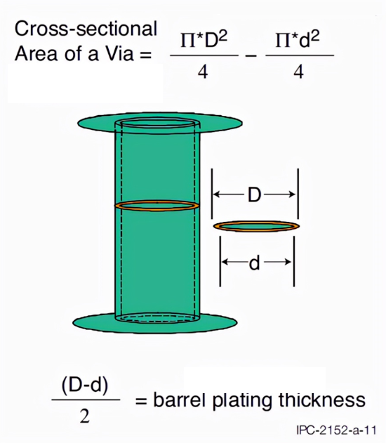
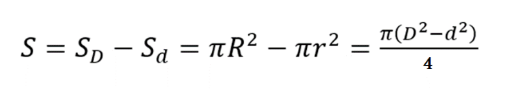
The figure below is the calculation chart of the cross-sectional area of the through-hole given by IPC 2152. The formula of the cross-sectional area of the through-hole wall in the above figure is transformed, where D is the empty outer diameter, D is the inner diameter of the hole, and (d-d)/2 is the thickness of the hole wall, also known as the through-hole copper thickness. Where D is the empty outer diameter, D is the inner diameter of the hole, and (d-d)/2 is the thickness of the hole wall, also known as the thickness of copper through the hole. The copper thickness through the hole is not determined, and the copper thickness of each PCB manufacturer may be different. If you want to pass a larger current through the hole, it may be better to punch several more through the hole.
Then you can get a new formula of calculating cross sectional area of hole wall:
A typical example is calculating the via size based on a 20°C temperature rise and a 1A current.
Given:
Copper thickness of 1 oz (1.38 mil)
Current carrying capacity of 1A
Maximum temperature rise of 20°C
From the IPC-2152 Conservative Chart, the cross-sectional area corresponding to these conditions is 28 mil². Using the equation for the via’s cross-sectional area, you can calculate the via’s diameter.
From the chart, the required cross-sectional area is 28 mil².
The copper thickness is 1.38 mil.
Solving for the via diameter, we get:
d = 7.28 mil (0.185 mm)
Thus, a via with an internal diameter of 0.185 mm will safely carry a 1A current with a 20°C temperature rise.
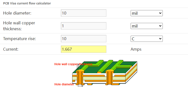
EBest Circuit (Best Technology)’s Via Current Capacity Calculator
EBest Circuit (Best Technology) offers a current capacity calculator for PCB vias to ensure that designs meet specific current-carrying needs. The tool allows designers to input their parameters, such as via diameter and copper thickness, and outputs the current-carrying capacity value. Clik below image to use or click here: via current capacity calculator