What is the capacity of a circuit?
The capacity of a circuit, often referred to as PCB current-carrying capacity, is the maximum amount of electrical current it can handle without overheating or causing a fault. This capacity is crucial for ensuring that the circuit operates safely, powering all connected devices without causing damage. A circuit’s capacity is typically measured in amperes (amps), which shows the flow of electrical current. The capacity of a circuit is determined by its components, such as the wire size, the circuit breaker, and the connected devices.

Circuits need to be designed and maintained within their safe capacity. If you overload a circuit, it could lead to overheating, equipment failure, or even an electrical fire. The circuit breaker is the main defense against this, as it cuts off the current flow if the circuit exceeds its capacity.
How can an electrician predict a circuit’s capacity?
Electricians can predict a circuit’s capacity by analyzing the components of the electrical system. The wire gauge, breaker rating, and the types of devices connected to the circuit are all factors in this determination. The wire gauge (or thickness) is one of the most important factors—thicker wires can carry more current.
Another key element is the circuit breaker or fuse. These devices are rated for a specific current. For example, a typical household circuit breaker may be rated for 15 or 20 amps. Electricians calculate the expected load, considering how many devices are likely to run on that circuit at the same time.
To predict the capacity accurately, electricians follow safety codes and standards like the National Electrical Code (NEC). This ensures that the circuits can handle the loads without risks of overload.
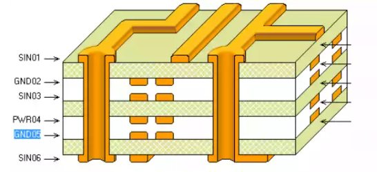
What determines the size of a circuit?
The size of the circuit is mainly determined by the supply voltage and resistance.
The size of the current is affected by a number of factors, of which the power supply voltage and resistance are the most direct and critical factors. The power supply voltage directly determines the driving force of the electron flow in the circuit, and the resistance is the obstacle of the electron flow, and the two work together to determine the size of the current in the circuit. To be specific:
Power supply voltage
The power supply voltage directly affects the size of the current. According to Ohm’s law, current is proportional to voltage. This means that the higher the voltage, the greater the current in the circuit.
Resistance size
The larger the resistance, the less current passes through the circuit. According to Ohm’s law, current is inversely proportional to resistance. This means that the greater the resistance, the smaller the current in the circuit.
In addition, the series-parallel relationship of the circuit and the temperature also affect the size of the current. In a series circuit, the total current is equal to the sum of the currents of each resistor; In a parallel circuit, the total current is also the sum of the individual resistance currents. A change in temperature will affect the value of the resistance and thus the magnitude of the current.
What is the making capacity of the circuit?
The making capacity of a circuit refers to the ability of a breaker or switch to handle the initial surge of current when it is first energized. This initial surge, often called inrush current, can be much higher than the normal operating current. The making capacity is crucial because it ensures that the breaker can handle this brief spike without tripping unnecessarily.
In industrial applications, the making capacity is even more important, as many machines and motors draw a high inrush current when starting up. The breaker must be able to manage this surge without interrupting the power flow. Typically, the making capacity is higher than the breaker’s rated current capacity to account for these surges.
What determines circuit capacity?
The factors that determine the capacity of a circuit mainly include the structure of the capacitor itself, environmental conditions, and application scenarios. The structure of the capacitor is a key factor in determining its capacity, specifically including:
- Distance between the plates
The smaller the distance between the plates, the greater the capacitance. This is because reducing the distance increases the electric field strength, allowing the capacitor to store more charge.
- Relative area of the plates
The larger the relative area of the plates, the greater the capacitance. A larger area makes the electric field more uniform, thus increasing the capacitor’s capacitance.
- Dielectric constant of the insulating material
The higher the dielectric constant of the insulating material, the greater the capacitance of the capacitor. The dielectric constant reflects the material’s ability to influence the electric field, affecting the capacitor’s capacitance.
- Material of the metal plates
The material of the metal plates also affects the capacitance. Factors such as the purity and conductivity of the metal can influence the capacity. Higher purity and better conductivity in the metal plates can increase the electric field strength, thus enhancing the capacitor’s capacitance.
Environmental conditions and application scenarios can also affect the circuit’s capacity, including:
- Ambient temperature
Changes in ambient temperature can affect the resistivity of the metal plates and insulating material, which in turn affects the capacitance. An increase in temperature typically lowers resistivity, which may either increase or decrease capacitance, depending on how temperature influences resistivity.
- Load resistance
In practical applications, when the capacitor works together with load resistance, the size of the load resistance affects the capacitor’s charging and discharging process, thereby influencing its capacitance. The size of the load resistance determines the speed at which the capacitor stores and releases charge, thus impacting the capacitor’s performance.
How do you calculate circuit load capacity?
To calculate circuit load capacity, electricians follow a few simple steps. First, they determine the total wattage of all the devices on the circuit. For example, a room may have several light bulbs, a television, and a computer, each with their own wattage rating.
Once they have the total wattage, they divide this by the voltage (typically 120V in homes). This gives them the total current in amps that the circuit is using. Electricians then compare this value to the circuit breaker’s rating. For safety, the total load should not exceed 80% of the breaker’s capacity. So, on a 20-amp circuit, the maximum continuous load would be 16 amps.
What is the maximum load on a 20-amp breaker?
A standard 20-amp breaker can handle up to 2,400 watts, based on a 120V system (20 amps x 120 volts = 2,400 watts). However, the NEC recommends only using 80% of the breaker’s capacity for continuous loads. That means a 20-amp breaker should typically handle no more than 1,920 watts (80% of 2,400 watts) for ongoing use.
This buffer is important because many appliances and devices draw more power when they first turn on, especially if they have motors or heating elements. By keeping the load below 80%, you avoid overloading the circuit.
In practical terms, a 20-amp breaker is commonly used for kitchen appliances like microwaves, toasters, or coffee makers. It’s also used in rooms where many devices might be connected, like living rooms or offices. By calculating the load and making sure it stays below the maximum, you can safely use your circuit without causing it to trip.