Looking for PCB manufacturer in Bosnia and Herzegovina? This guide covers full-process guarantee, best tech selection, top 10 manufacturers, choosing methods, and evaluating production & delivery time.
When searching for a reliable PCB manufacturer in Bosnia and Herzegovina, many clients face challenges in balancing quality, delivery time, and cost. This blog comprehensively sorts out the top 10 PCB manufacturers in Bosnia and Herzegovina, analyzes core pain points in local PCB prototyping, manufacturing, and design, and provides professional solutions. Whether you are looking for a local manufacturer or an international partner with strong strength, this guide will help you make informed decisions. As a professional PCB Manufacturer in Bosnia and Herzegovina – related service provider, we are committed to solving your PCB production problems with comprehensive strength and thoughtful service.
Are You Facing the Following Problems?
- Is the prototyping cycle too long to meet the urgent project progress requirements?
- Do you face unstable product quality with frequent solder mask peeling and line short-circuit problems?
- Is the lack of professional design technical support leading to repeated modifications and increased costs?
- Are the pricing non-competitive and lack targeted cost-saving solutions for different project scales?
- Does unclear delivery time commitment often cause delayed delivery that affects the overall project schedule?
- Is the incomplete quality inspection process resulting in unqualified products entering the market and causing losses?
Full-Process Guarantee from Requirement to Delivery
- Urgent prototyping service: 24-hour rapid prototyping to solve the problem of tight project progress.
- Strict quality control system: Full inspection for mass production, eliminating quality problems such as solder mask peeling and line short-circuit.
- Professional technical team: Provide one-stop technical support from design to production, avoiding repeated modifications.
- Personalized cost-saving solutions: Formulate competitive pricing strategies according to project scale and requirements.
- Clear delivery commitment: 99.2% on-time delivery rate, with special logistics plans for urgent orders to ensure on-time delivery.
- Comprehensive after-sales service: Track the use of products, and quickly respond to and solve any quality problems that arise.
Why Choose EBest Circuit (Best Technology) for PCB Manufacturer?
Reasons Why Choose EBest Circuit (Best Technology) for PCB Manufacturer:
- Cost-Optimized Solutions: Customize cost-sensitive plans for diverse designs, slashing production costs significantly while maintaining quality to boost your project profitability.
- 24-Hour Urgent Prototyping Guarantee: Accelerate your project cycle with rapid prototyping for urgent orders—get valid samples in just one day to verify designs and seize market opportunities ahead of schedule.
- Reliable Fast Delivery: Boasting a 99.2% on-time delivery rate, we leverage a robust logistics network to ensure every order arrives precisely as scheduled, eliminating project delays caused by late shipments.
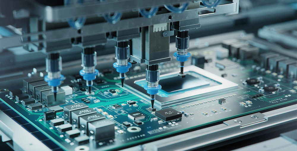
- Premium Quality Assurance: Implement 100% full inspection for mass production, with a strict three-stage quality control process (raw material inspection → in-process monitoring → finished product testing) to ensure zero defective products enter the market.
- 19 Years of Industry Expertise & Error Database: Draw on nearly two decades of production experience; our exclusive error database helps avoid repeated mistakes, reducing rework costs and improving project efficiency.
- Free Professional DFM Analysis: Get complimentary design for manufacturability analysis to optimize layouts, resolve potential production issues in advance, and enhance production yield while cutting modification costs.
- Comprehensive Authoritative Certifications: Hold ISO9001:2015, ISO13485:2016, REACH, RoHS, IATF16949 certifications—our products meet global industry standards, ensuring compliance and reliability for your global market expansion.
- Tailored One-Stop Solutions: Customize end-to-end production plans based on your unique project requirements, perfectly matching diverse production needs from small batches to mass production.
Top 10 PCB Manufacturer in Bosnia and Herzegovina
| Company Name | Main Business | Core Advantages | Process Capability | Delivery Time |
| EBest Circuit (Best Technology) Co.,Ltd | PCB prototyping, mass production, PCB design optimization, DFM analysis | 19 years of production experience, 24-hour rapid prototyping, 99.2% on-time delivery rate, complete international certifications, free DFM analysis | Supports single-sided, double-sided, multi-layer PCB (up to 32 layers), HDI, rigid-flex PCB; min. line width/spacing 3mil/3mil, min. hole diameter 0.1mm | Prototyping: 24-72 hours; Mass production: 5-12 working days |
| Bosna PCB d.o.o. | Single-sided and double-sided PCB manufacturing, PCB assembly | Localized production/service, fast response to local clients, competitive pricing for small/medium batches | Single-sided/double-sided PCB; min. line width/spacing 6mil/6mil, min. hole diameter 0.2mm | Prototyping: 5-7 working days; Mass production: 10-15 working days |
| Sarajevo Electronics Manufacturing d.o.o. | Multi-layer PCB manufacturing, PCB testing, small-batch PCB assembly | Professional testing equipment, strict quality control, good cooperation with local component suppliers | Supports up to 8-layer PCB; min. line width/spacing 4mil/4mil, min. hole diameter 0.15mm | Prototyping: 3-5 working days; Mass production: 7-12 working days |
| Zenica PCB Solutions d.o.o. | PCB prototyping, custom PCB manufacturing, PCB repair | Flexible production, personalized customization, fast after-sales response | Single-sided, double-sided, 4-layer PCB; min. line width/spacing 5mil/5mil, min. hole diameter 0.18mm | Prototyping: 4-6 working days; Mass production: 8-14 working days |
| Tuzla Printed Circuits d.o.o. | Mass production of double-sided/multi-layer PCB, PCB surface treatment | Large-scale production capacity, stable quality, competitive mass order pricing | Supports up to 12-layer PCB; min. line width/spacing 4mil/4mil, min. hole diameter 0.12mm | Prototyping: 5-7 working days; Mass production: 6-10 working days |
| Banja Luka PCB Tech d.o.o. | PCB prototyping, small-batch production, PCB design consulting | Professional design consulting team, technical support for PCB design, high prototyping precision | Single-sided, double-sided, 6-layer PCB; min. line width/spacing 3.5mil/3.5mil, min. hole diameter 0.1mm | Prototyping: 2-4 working days; Mass production: 9-13 working days |
| Mostar Electronics Components d.o.o. | PCB manufacturing, PCB assembly, supply of supporting electronic components | One-stop PCB manufacturing/assembly service, convenient component sourcing | Single-sided, double-sided, 8-layer PCB; min. line width/spacing 5mil/5mil, min. hole diameter 0.16mm | Prototyping: 5-6 working days; Mass production: 10-15 working days |
| Cazin PCB Manufacturing d.o.o. | Customized PCB manufacturing, high-temperature resistant PCB production, PCB testing | Specialized in high-temperature PCB, strong technical strength in special materials, strict testing standards | Double-sided/multi-layer high-temperature PCB (up to 10 layers); min. line width/spacing 4mil/4mil, min. hole diameter 0.14mm | Prototyping: 6-8 working days; Mass production: 12-16 working days |
| Brcko PCB Services d.o.o. | PCB prototyping, small/medium batch production, PCB maintenance/modification | Low small-batch order threshold, flexible pricing, fast maintenance response | Single-sided/double-sided PCB; min. line width/spacing 6mil/6mil, min. hole diameter 0.2mm | Prototyping: 3-5 working days; Mass production: 11-16 working days |
| Trebinje Advanced Circuits d.o.o. | HDI PCB manufacturing, multi-layer high-precision PCB production, PCB design optimization | Advanced equipment, strong high-precision PCB capability, professional design optimization team | HDI PCB, up to 16-layer high-precision PCB; min. line width/spacing 2.5mil/2.5mil, min. hole diameter 0.08mm | Prototyping: 4-7 working days; Mass production: 8-13 working days |
How to Choose a PCB Manufacturer in Bosnia and Herzegovina?
Selection Guide to PCB Manufacturer in Bosnia and Herzegovina:
1. Verify technical and process capabilities: Confirm if the manufacturer’s PCB layer support, minimum line width/line spacing, and hole diameter specifications match your project requirements; it’s recommended to request sample verification for key processes.
2. Inspect quality control systems and certifications: Check if the manufacturer has complete quality management systems (such as ISO9001, IATF16949) and valid certification documents; review their quality inspection reports and defect rate data.
3. Clarify delivery commitments and reliability: Confirm the official on-time delivery rate, standard delivery cycles for different order types (prototyping, mass production), and emergency response plans for urgent orders.
4. Evaluate pricing rationality and cost-saving potential: Understand the pricing structure to avoid hidden costs; confirm if personalized cost-saving solutions can be provided based on project scale and design requirements.
5. Assess after-sales service level: Investigate the response speed to quality problems, the effectiveness of solution implementation, and whether there is a complete after-sales tracking mechanism.
6. Verify industry experience and market reputation: Check the manufacturer’s years of production experience, typical project cases, and client feedback to ensure reliable cooperation performance.
7. Confirm technical support capabilities: Ensure the manufacturer can provide value-added services such as free DFM analysis and design optimization to reduce modification costs and improve production yield.
8. Evaluate production flexibility and scalability: Confirm if the manufacturer can adapt to changes in order quantity (from small batches to mass production) and meet potential future project expansion needs.
How to Evaluate the Production Capacity of Bosnia and Herzegovina PCB Manufacturer?
Evaluation Guide to the Production Capacity of Bosnia and Herzegovina PCB Manufacturer:
- Check the manufacturer’s production equipment configuration, including whether it has advanced PCB manufacturing and testing equipment.
- Understand the manufacturer’s maximum production capacity and monthly output to confirm whether it can meet the demand for mass orders.
- Evaluate the manufacturer’s process coverage, such as whether it can produce single-sided, double-sided, multi-layer, HDI and other types of PCB.
- Investigate the manufacturer’s raw material supply chain stability to ensure the continuous supply of production materials.
- Check the manufacturer’s quality inspection reports and defect rate data to reflect its production quality control level.
- Understand the manufacturer’s technical team strength, including the number of professional and technical personnel and their experience.
- Confirm whether the manufacturer has the ability to handle special requirements, such as high-temperature resistant, waterproof and other special PCB production.
How to Evaluate the Delivery Time of PCB Manufacturer in Bosnia and Herzegovina?
Evaluation Guide to the Production Capacity of PCB Manufacturer in Bosnia and Herzegovina:
- Obtain the manufacturer’s official delivery time commitment for different types of orders (prototyping, small batch, mass production).
- Investigate the manufacturer’s historical on-time delivery rate data to verify the credibility of the delivery time commitment.
- Understand the manufacturer’s production scheduling system and whether it has a special plan for urgent orders.
- Check the manufacturer’s logistics and distribution partners to confirm the efficiency and stability of the logistics link.
- Evaluate the manufacturer’s ability to respond to unexpected situations, such as whether it can adjust the production schedule in time when encountering raw material shortages.
- Confirm whether the manufacturer has a clear compensation mechanism for delayed delivery.
- Communicate with the manufacturer to understand the key links affecting the delivery time and their control measures.
FAQs About Bosnia and Herzegovina PCB Manufacturing
Q1: What is the preferred solution for PCB prototyping in Bosnia and Herzegovina?
A1: FabLab BiH’s rapid prototyping lab is the local top choice. It integrates 3D printing, CNC machining, and PCB design capabilities, completing complex multi-layer board prototypes within 1-2 months. Specialized in mechanical-electronic system integration, it has provided rapid verification services for European research projects.
Q2: What are the core challenges facing Bosnia and Herzegovina’s PCB manufacturing industry?
A2: Key challenges include logistics time fluctuations (3-5 days for overland transport to Western Europe), incomplete local supply chains (reliance on imported high-end substrates), and varying process standardization levels. Advantages include 30%-40% lower labor costs than Western Europe and compliance with EU environmental standards, making it suitable for small-to-medium batch orders.
Q3: Which PCB manufacturers in Bosnia and Herzegovina are worth noting?
A3: Any PCBA and H.C.C. INTERNATIONAL LIMITED are active local players. The former offers end-to-end solutions from design to assembly, while the latter holds patents in metal substrate technology. Note that some “local companies” are subcontractors for international brands, so verify production locations.
Q4: How to ensure quality stability in Bosnia and Herzegovina PCB manufacturing?
A4: Prioritize factories certified to ISO 9001/14001 standards. Focus on surface treatment processes (e.g., ENIG plating thickness test reports) and interlayer alignment accuracy. Request IPC-A-600 standard test reports and consider X-ray inspection for first orders to verify quality.
Q5: What emerging trends exist in the country’s PCB industry?
A5: Green manufacturing is rising, with multiple factories adopting lead-free soldering and recyclable substrates. High-frequency substrate processing capabilities are improving amid growing 5G equipment demand. Local research institutions are collaborating with German firms to develop smart factory systems, predicting an automation line upgrade wave post-2026.