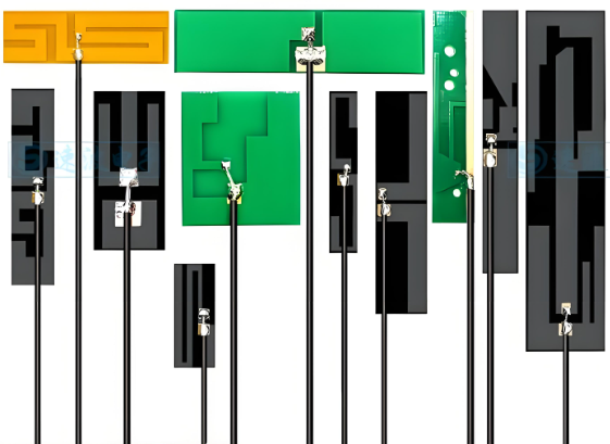
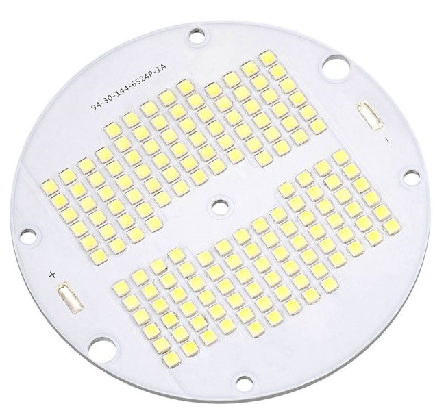
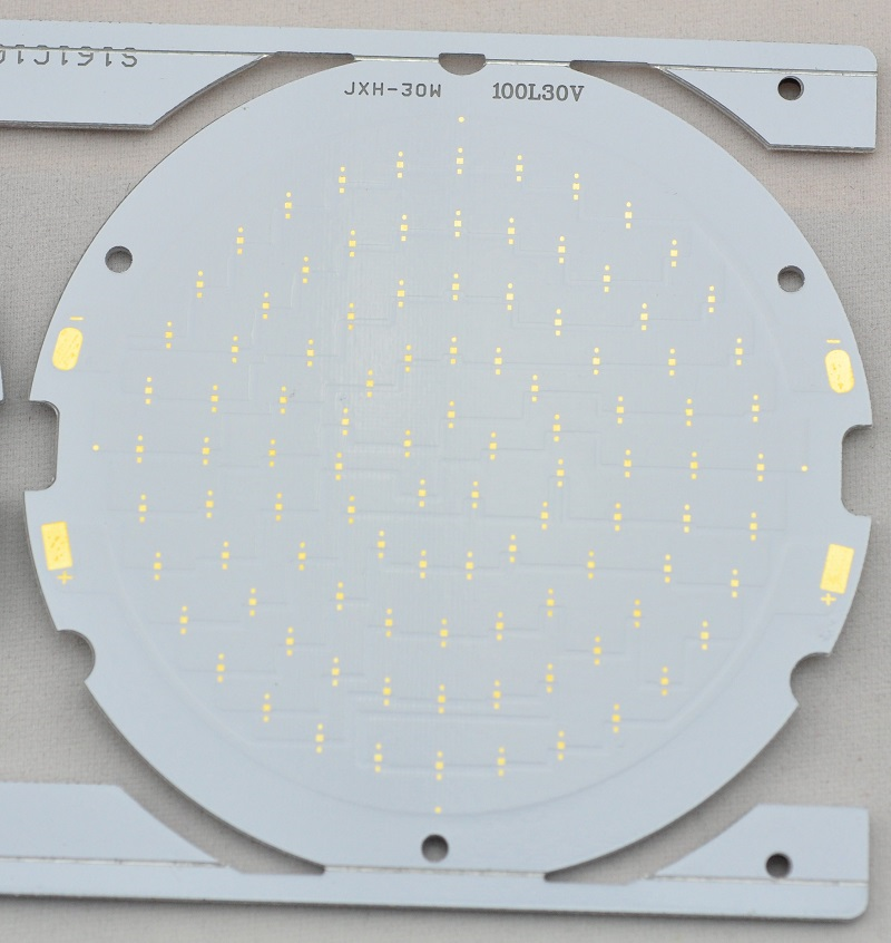
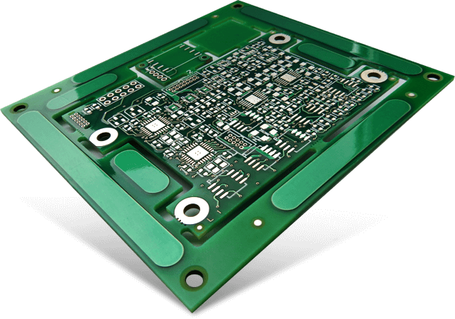
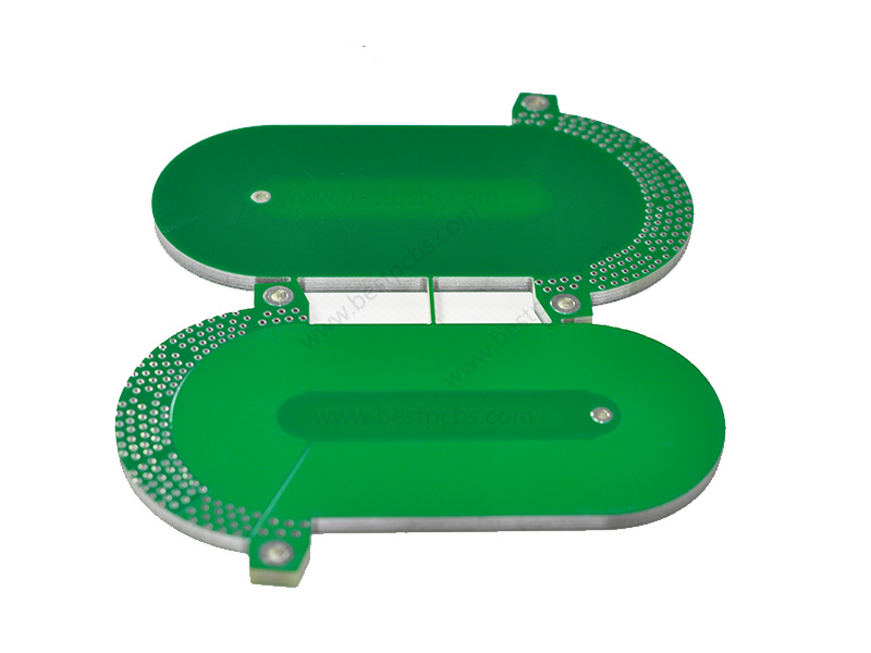
Special PCB is a customized circuit board designed for unique applications where standard PCBs do not meet the required performance, durability, or environmental conditions. These PCBs are used in industries such as aerospace, medical, telecommunications, and automotive, where factors like heat dissipation, high frequency, and miniaturization are crucial. Whether it’s a high-speed PCB, HDI PCB, or heavy copper PCB, each type serves a specific purpose to enhance electronic performance.
EBest Circuit (Best Technology) excel in providing customer-centric support in PCB industry. The team offers special PCB design optimization, material selection guidance, and manufacturing feasibility analysis to the customers. Whether you need a special PCB prototype or full-scale special PCB manufacturing, just feel free to reach out to us at sales@bestpcbs.com, we work closely with you to meet your exact specifications.
What is Special PCB?
A special PCB is a customized printed circuit board that differs from standard PCBs in design, materials, or functionality. It is engineered to meet specific requirements such as high power handling, extreme temperatures, or unique form factors. These boards ensure stability, reliability, and efficiency in demanding applications.
What Are the Different Types of Special PCBs?
Special PCBs can be classified into three main categories based on their materials, functionality, and structure.
1) Material-Based Special PCBs
These PCBs are defined by the materials used to enhance their performance under specific conditions.
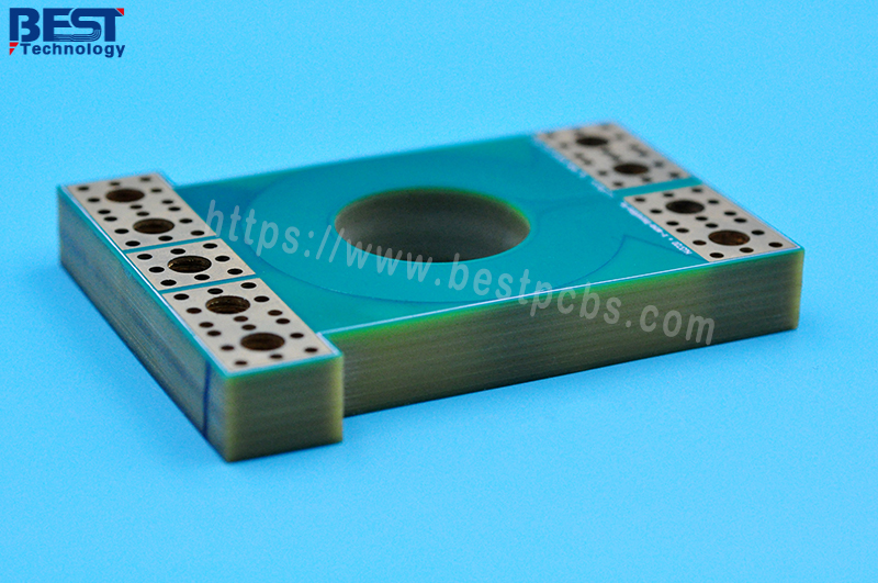
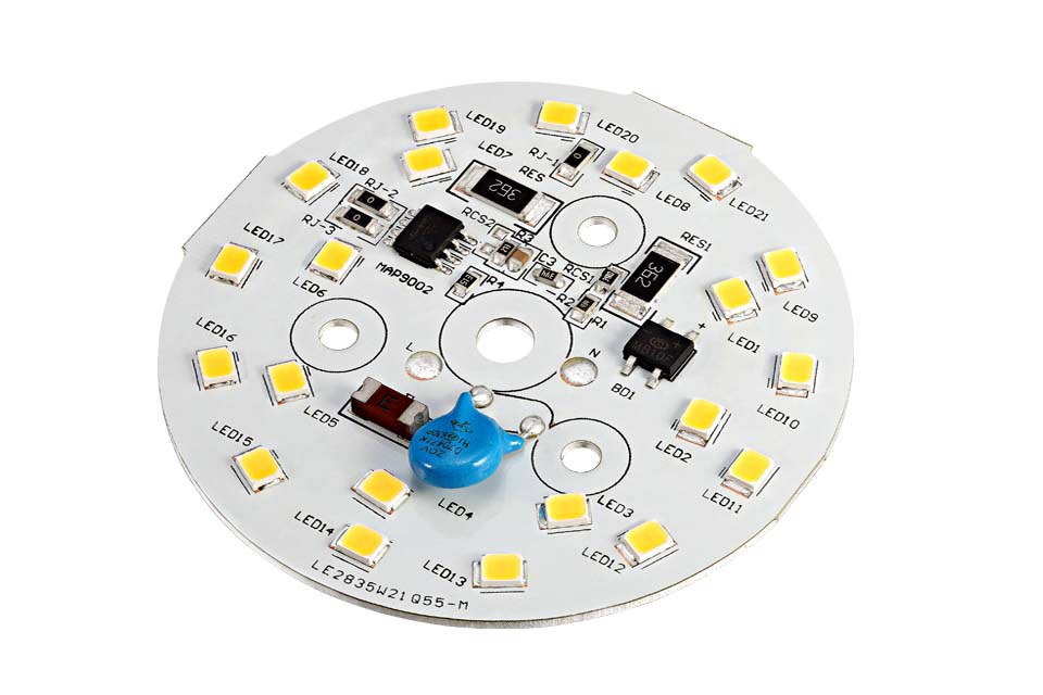
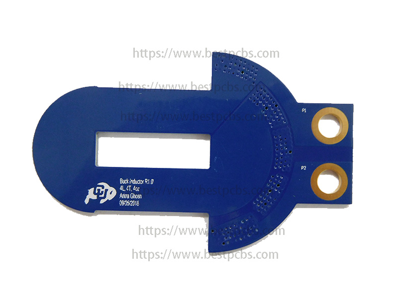
Heavy Copper PCB – Uses thick copper layers (≥3 oz) for high current applications and improved thermal management.
High Tg PCB – Made with high glass transition temperature (Tg) materials to withstand extreme heat and mechanical stress.
2) Function-Based Special PCBs
This category includes PCBs designed for specific electrical or performance characteristics.
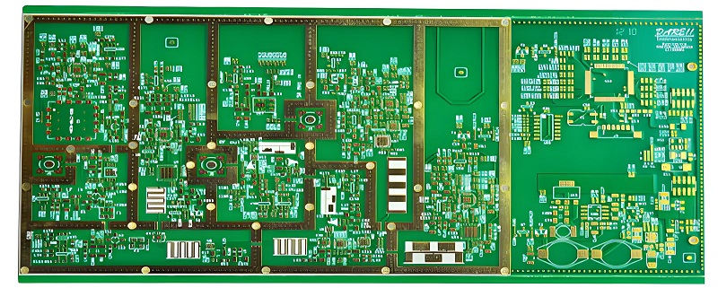
High-Speed PCB – Designed with low-loss materials and controlled impedance for fast signal transmission in networking and computing.
Impedance Control PCB – Maintains precise impedance levels for RF, microwave, and high-frequency circuits.
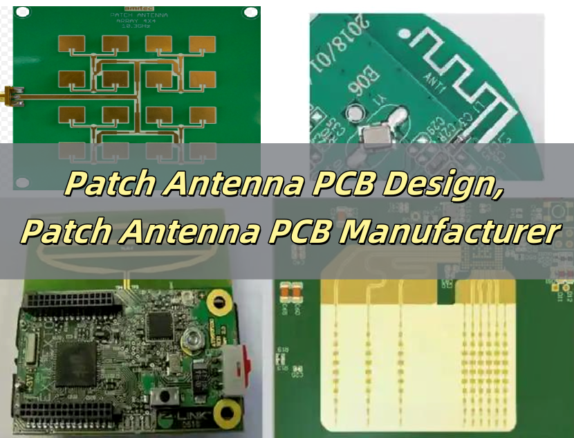
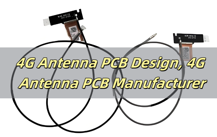
RF Board – Uses low-loss materials to minimize signal interference in wireless communication, radar, and satellite applications.
Bus Bar PCB – Incorporates embedded copper bars for high current carrying capacity in power distribution systems.
3) Structure-Based Special PCBs
These PCBs are categorized based on their physical design and layout innovations.
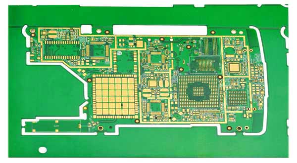
HDI PCB – Features microvias, fine traces, and multiple layers for compact, high-density applications like smartphones and laptops.
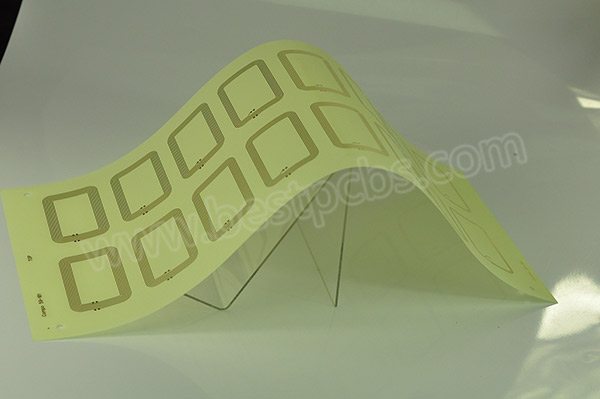
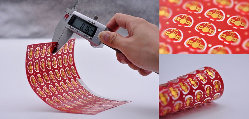
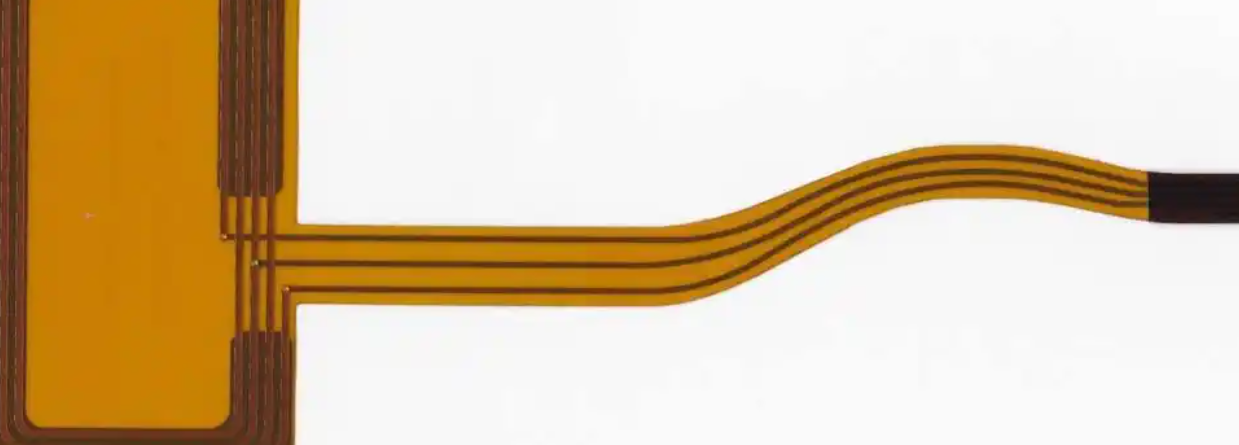
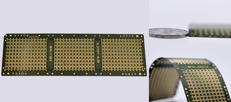
Extra Thin PCB – Ultra-thin boards designed for compact and flexible electronic devices.
IC Substrate – Specialized interconnects used to bridge semiconductor chips with larger PCB assemblies.
What Materials Are Used to Make Special PCBs?
The choice of materials in special PCBs determines their electrical performance, heat resistance, and mechanical durability. Here are the key materials used:
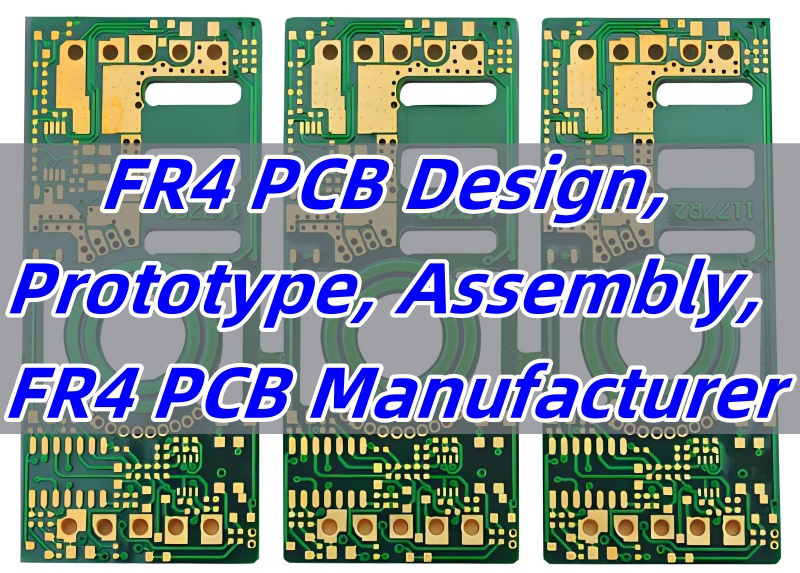
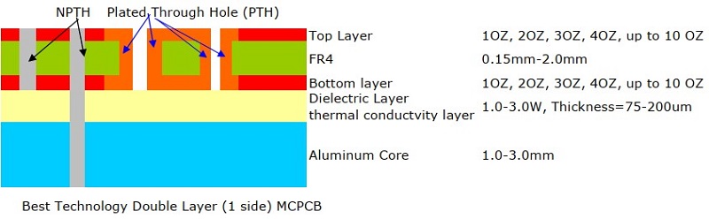
1) FR-4
A fiberglass-reinforced epoxy laminate that offers a balance of cost, durability, and electrical insulation. It is commonly used in High Tg PCBs, HDI PCBs, and Impedance Control PCBs where thermal resistance and signal integrity are crucial.
2) High-Tg FR-4
An advanced version of FR-4 with a higher glass transition temperature (Tg), making it suitable for High Tg PCBs and High-Speed PCBs that operate under extreme thermal conditions.
3) Polyimide
This material provides exceptional thermal stability and flexibility. It is widely used in Extra Thin PCBs and HDI PCBs, where space-saving and durability under heat are essential.
4) PTFE (Teflon)
A low-loss, high-frequency material that is ideal for RF Boards and High-Speed PCBs. Its excellent dielectric properties help maintain signal integrity in wireless and microwave applications.
5) Copper
- Heavy Copper PCB – Uses thick copper layers (≥3 oz) to support high current loads and enhance heat dissipation.
- Bus Bar PCB – Features embedded copper bars for efficient power distribution in industrial and automotive applications.
6) BT (Bismaleimide Triazine) Epoxy Resin
This material is used in IC Substrates for its excellent electrical insulation, high-temperature resistance, and mechanical strength. It ensures reliable connections in semiconductor packaging.
7) Low-Dk (Low Dielectric Constant) and Low-Df (Low Dissipation Factor) Materials
These are specialized dielectric materials used in Impedance Control PCBs and High-Speed PCBs to reduce signal loss and maintain consistent impedance for high-frequency applications.
How to Design a Special PCB?
1) Define Requirements
Start by determining the electrical, thermal, and mechanical specifications needed for the application.
2) Select Materials
Choose the right substrate, copper thickness, and surface finish based on operating conditions and performance needs.
3) Create a Schematic
Develop a circuit diagram to define component placement and electrical connections.
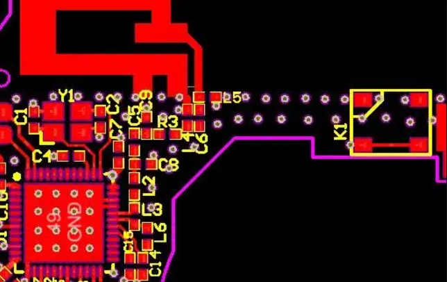
4) Layout Design
Optimize routing, layer stack-up, and impedance matching to ensure signal integrity and manufacturability.
5) Prototyping & Testing
Before mass production, test a prototype to validate functionality, thermal management, and reliability.
What Are the Benefits of a Special PCB?
1) High Performance
Custom designs ensure superior electrical and thermal efficiency.
2) Enhanced Durability
Robust materials and specialized coatings increase lifespan, even in harsh environments.
3) Miniaturization
Advanced designs, such as HDI and extra thin PCBs, enable compact, lightweight devices.
4) Reduced Signal Loss
Impedance control and RF materials enhance signal integrity, crucial for high-speed and wireless applications.
What Are the Applications of Special PCBs?
1) Aerospace & Defense
Used in satellite systems, avionics, and military-grade electronics that require reliability under extreme conditions.
2) Automotive Electronics
Essential for EV power systems, engine control units, and ADAS (Advanced Driver Assistance Systems).
3) Medical Devices
Supports high-precision diagnostic equipment, wearable health monitors, and implantable devices.
4) Telecommunications
Used in 5G infrastructure, networking hardware, and high-speed data transmission systems.
Why Choose EBest Circuit (Best Technology) as Your Special PCB Manufacturer?
1) Industry Expertise
With 18 years of experience, EBest Circuit (Best Technology) specializes in manufacturing high-quality special PCBs tailored to unique requirements.
2) Multi-Variety PCB Manufacturing
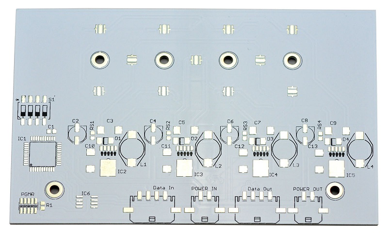
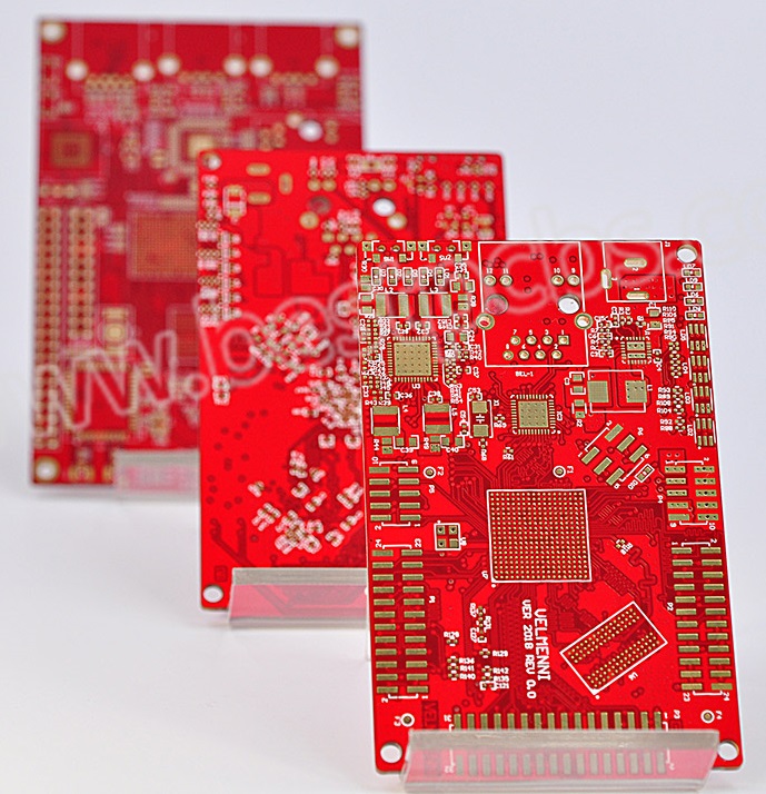
Electronics manufacturers often require diverse PCB types within a single project. EBest Circuit (Best Technology) offers a wide range of special PCBs, including Heavy Copper, Bus Bar, High-Speed, IC Substrate, Impedance Control, Extra Thin, High Tg, HDI, and RF Boards. Our ability to handle multiple PCB types under one roof simplifies the supply chain, reduces lead times, and ensures consistency across different PCB designs.
3) High Quality
Each special PCB undergoes rigorous testing to meet international quality and reliability standards.
4) Custom Solutions
As a leading special PCB manufacturer, we offer complete customization based on your project needs from special PCB design to special PCB assembly. Not only provide top quality requirements of Special Printed circuit Board and PCBA service for the market but also meet customer special customized requests.
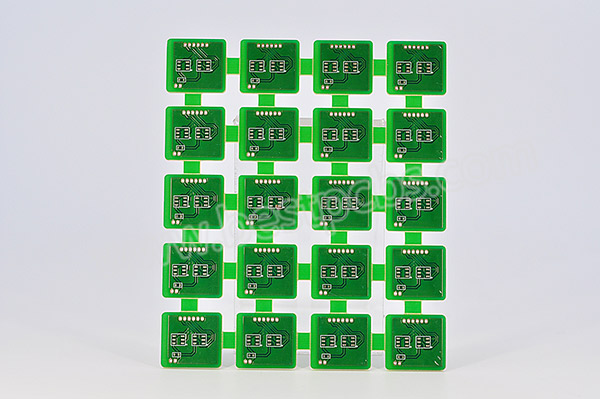
Small-Batch Production
At EBest Circuit (Best Technology), we specialize in low-volume special PCB manufacturing, ensuring that even small orders receive the same level of precision and quality as mass production. This allows customers to test new designs, reduce risks, and accelerate product development.
FAQs Of Special PCB
1. What is the maximum operating temperature for PCBs?
Typically, the working temperature for standard PCB materials is 105-130°C. For high-temperature materials, such as those made with 7316D, the working temperature can reach 150-170°C. However, this material requires a higher MOQ.
2. Is the smallest copper trace width you can do 4mil?
Yes.
3. What PCB material brands do you use?
We use brands like Shengyi, KB, ITTEQ, GDM, and etc.
4. What is the maximum board size you can produce?
The maximum size we can produce is 610mm x 610mm.
5. What is the maximum copper thickness for a PCB?
We can produce a maximum copper thickness of 30oz (1050um).
In conclusion, special PCBs are essential for high-performance, reliable, and efficient electronic applications. Whether you need heavy copper PCBs for power applications or HDI boards for miniaturized devices, selecting the right manufacturer is crucial. EBest Circuit (Best Technology) provides industry-leading expertise, top-notch quality, and tailored solutions to ensure your project’s success. Pls feel free to contact us at sales@bestpcbs.com to get started on your special PCB requirements!