In our daily life, the electronics has been gradually infiltrated our lives. Between them, the PCB board plays an important role in it, and we must say, PCB is the foundational element of electronics. From the simplest gadgets to the most complex machinery, PCBs play a crucial role.
What is a PCB Board?
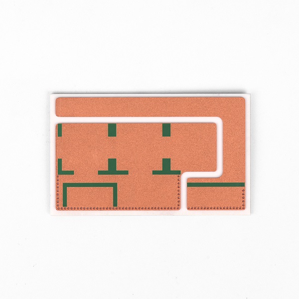
A printed circuit board (PCB) is an electronic that uses metal conductors to create electrical connections between components. Generally, a PCB is a flat, laminated composite made of non-conductive substrate materials with conductive pathways etched or printed onto it. These pathways, also known as traces, enable the electronic components mounted on the board to communicate with each other.
PCBs are designed to support and electrically connect various components such as resistors, capacitors, diodes, and integrated circuits. The intricate network of copper tracks forms circuits that dictate the device’s functionality. PCBs can range from simple single-sided boards used in basic electronics to complex multi-layered structures found in advanced applications.
Common PCB Structure
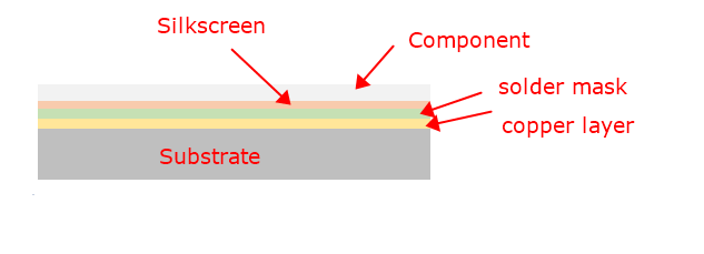
A PCB’s structure is composed of several key layers, each serving a distinct purpose. Here is a detailed breakdown of these layers:
Substrate (Base Material)
The substrate, usually made of fiberglass (FR4), provides the board with its rigidity and thickness. It is the foundational layer upon which all other materials are built.
Copper Layer
This conductive layer is typically made of copper foil. For single-sided PCBs, the copper layer is only on one side of the substrate, whereas double-sided and multi-layer PCBs have copper layers on both sides or between multiple layers of substrate.
Solder Mask
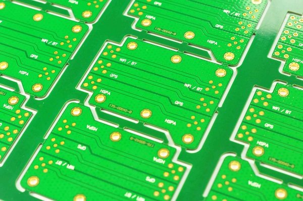
The solder mask is a protective layer applied over the copper traces to prevent oxidation and accidental short-circuiting. It insulates the copper traces and leaves the component pads exposed for soldering. The green color commonly associated with PCBs comes from this layer, though it can also be found in other colors like red, blue, black, and white.
Silkscreen
The silkscreen layer is used to add labels, symbols, logos, and other markings to the PCB. This layer helps in identifying component locations and orientations during assembly and troubleshooting.
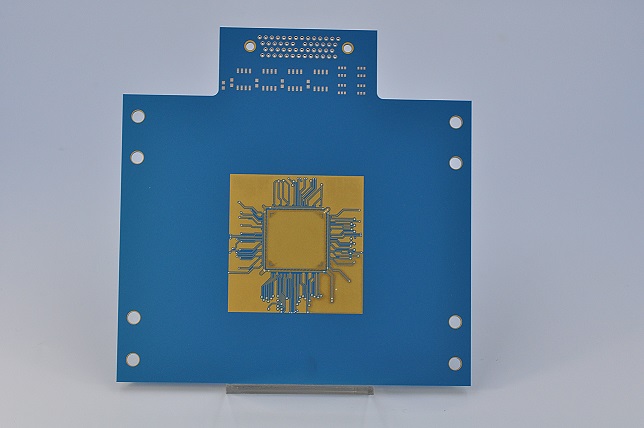
Components and Connectors (PCBA)
Components such as resistors, capacitors, diodes, and integrated circuits are soldered onto the PCB. Connectors allow the PCB to interface with other boards, power supplies, and external devices.
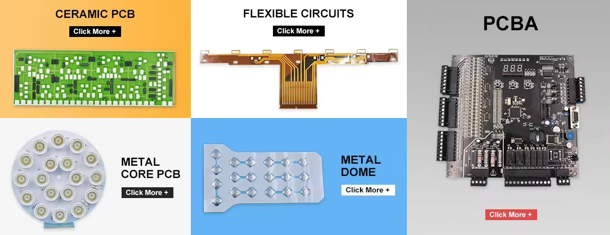
How Many Types of PCB?
Single-Sided PCBs
These are the simplest types of PCBs, with copper on only one side of the board. You’ll find them in basic, low-cost electronics like calculators, radios, and power supplies. They’re easy to design and manufacture, which keeps costs down and makes them great for straightforward applications.
Double-Sided PCBs
These boards have copper layers on both sides, allowing for more complex circuits. They’re common in more sophisticated electronics like amplifiers, power monitoring systems, and HVAC systems. With increased circuit density and flexible design options, they can handle more complex tasks.
Multi-Layer PCBs
When you need to pack in a lot of circuits, multi-layer PCBs are the way to go. They consist of three or more layers of copper, separated by insulating layers. You’ll see these in high-tech devices like computers, servers, medical equipment, and aerospace electronics. They offer high circuit density, reduced size and weight, and better signal integrity.
Rigid PCBs
Made from solid, inflexible materials like fiberglass, rigid PCBs keep their shape and provide strong support for components. They’re durable and used in everything from simple toys to complex industrial equipment.
Flexible PCBs
These are made from flexible plastic materials like polyimide, allowing them to bend and flex. Perfect for wearable electronics, flexible displays, and compact devices where space is tight. They’re lightweight, can fit into small, irregular spaces, and can handle being bent repeatedly.
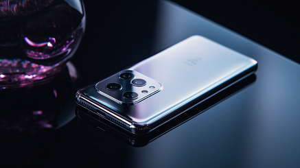
Rigid-Flex PCBs
Combining the best of both rigid and flexible PCBs, these are great for devices that need both stability and flexibility, like smartphones, cameras, and medical devices. They save space, reduce the need for connectors and interconnections, and improve reliability.
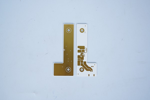
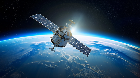
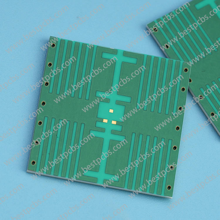
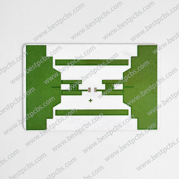
High-Frequency PCBs
Designed to operate at frequencies above 1 GHz, these are used in communication systems, microwave technology, and high-speed devices. They provide low signal loss and high performance, making them crucial for advanced communication technologies.
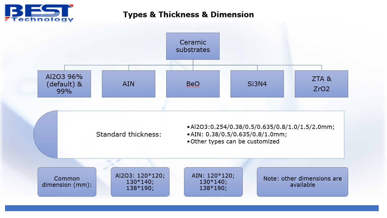
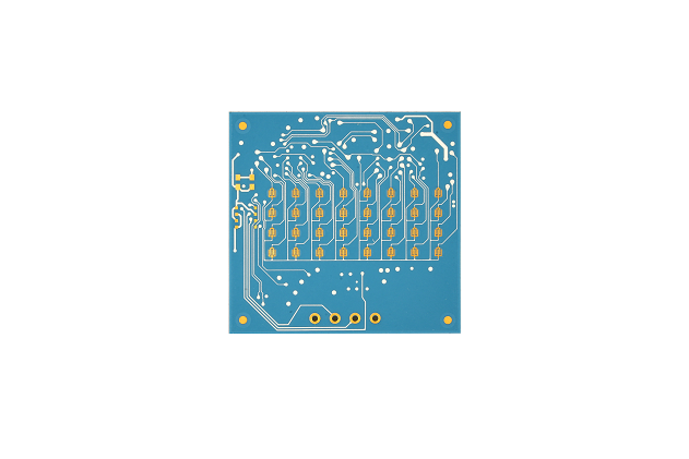
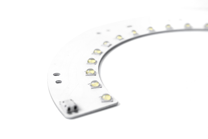
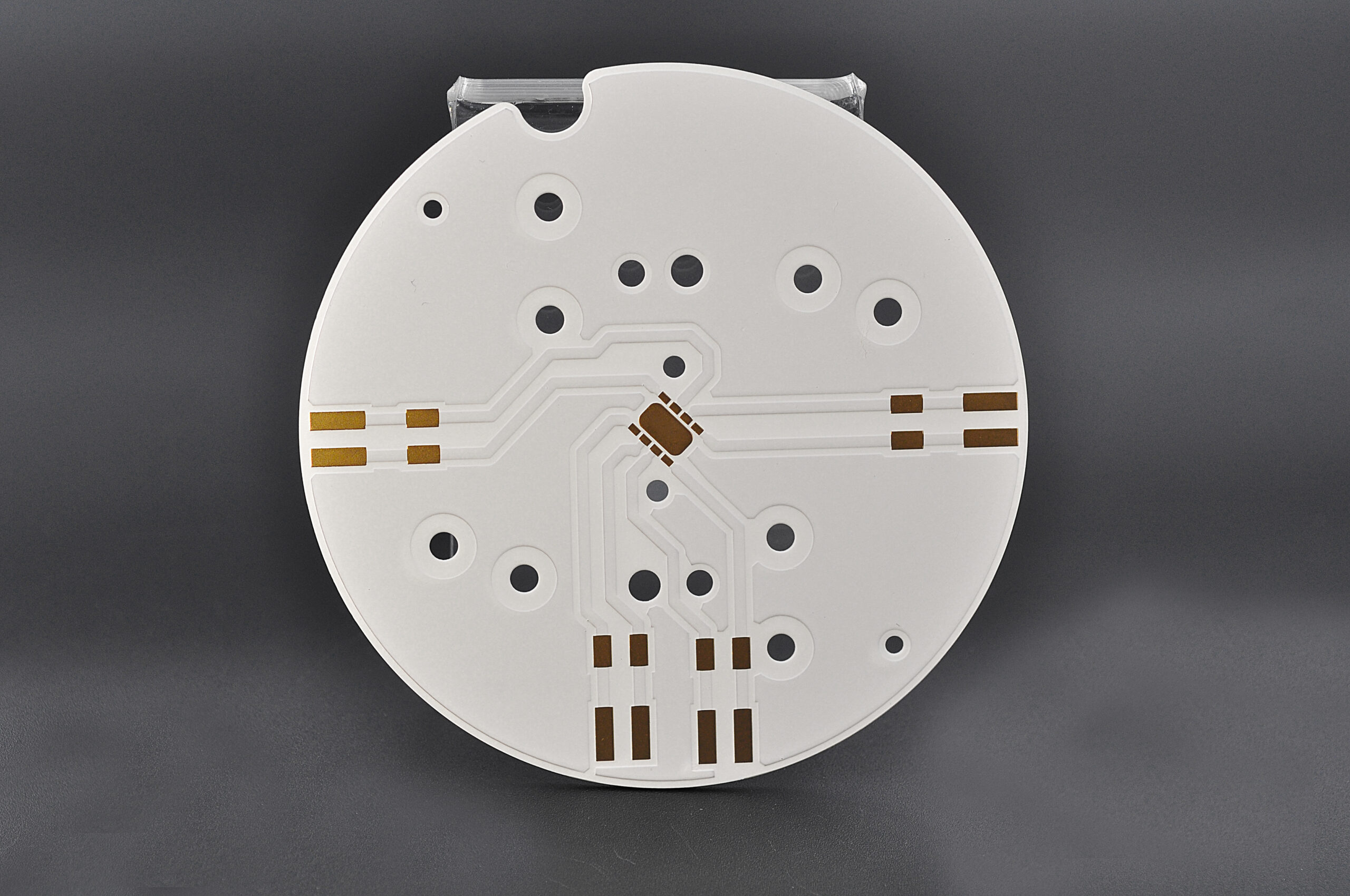
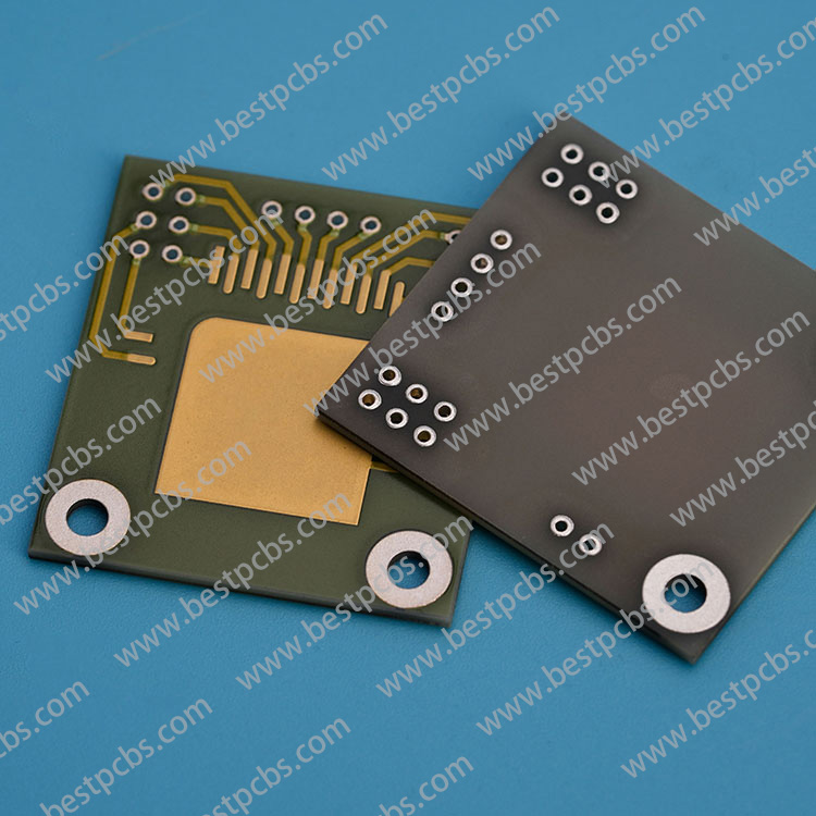
Ceramic PCBs
Using ceramic as the substrate material, these PCBs offer excellent thermal conductivity and stability. They’re perfect for high-power applications and environments with extreme temperatures, like LED lighting, power electronics, and aerospace systems. Ceramic PCBs ensure reliable performance in harsh conditions.
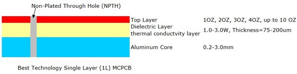
Metal Core PCBs
Featuring a metal core, usually aluminum or copper, these PCBs improve heat dissipation. They’re used in high-power applications where efficient thermal management is crucial, such as LED lighting, power supplies, and automotive electronics.
Special PCBs
Bus Bar PCBs
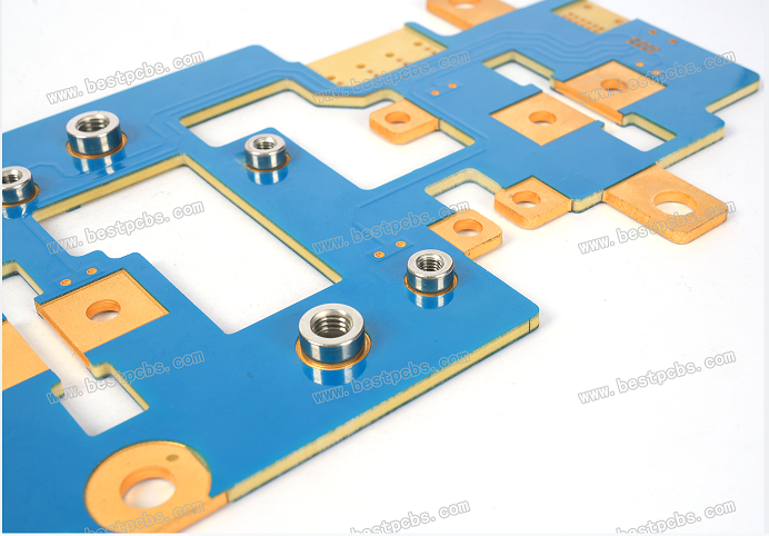
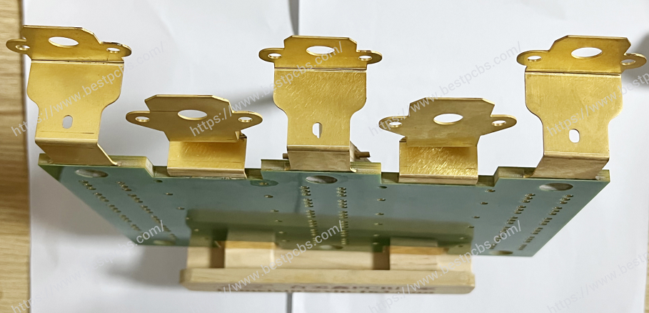
These integrate bus bars for high-current applications, ensuring efficient power distribution and minimal voltage drop. They’re used in heavy-duty power supplies, electric vehicles, and industrial machinery. Bus bar PCBs provide robust and reliable connections for high-power systems.
Heavy Copper PCBs
With thicker copper layers, typically 3 ounces per square foot or more, these PCBs can handle higher currents and enhance thermal management. They’re used in power distribution, automotive, and industrial applications where durability and performance are critical. Heavy copper PCBs ensure reliable operation under high-stress conditions.
HDI (High-Density Interconnect) PCBs
These feature finer lines and spaces, smaller vias, and higher connection pad density. They’re used in advanced electronics like smartphones, tablets, and medical devices where space and performance are paramount. HDI PCBs enable miniaturization and improved electrical performance.
Extra Thin PCBs
Designed with minimal thickness, these PCBs are perfect for fitting into compact and lightweight devices. You’ll find them in flexible displays, wearables, and miniaturized electronic gadgets. Extra thin PCBs allow for innovative design solutions and space-saving configurations.
RF (Radio Frequency) PCBs
Optimized for high-frequency signals, these are used in communication devices, antennas, and microwave applications. They’re designed to minimize signal loss and interference, ensuring optimal performance in wireless communication systems.
High Tg PCBs
These have a high glass transition temperature, making them suitable for high-temperature environments. Used in automotive, aerospace, and industrial applications, high Tg PCBs maintain structural integrity and performance at elevated temperatures.
Impedance Control PCBs
These are designed to maintain consistent impedance for high-speed signal transmission. They’re used in communication devices, high-speed digital circuits, and advanced computing systems. Impedance control PCBs ensure signal integrity and reduce signal loss and reflection.
Why Are PCB Boards So Expensive?
Material Quality
High-grade materials like FR4 (fiberglass), ceramics, and high-quality copper foil are used to ensure durability and performance. These materials are essential for withstanding environmental stress and ensuring reliable operation, but they are expensive. For example, ceramic substrates can cost up to 10 times more than standard FR4 materials due to their superior thermal conductivity and electrical properties.
Complexity of Design
Multi-layer PCBs and advanced designs such as HDI (High-Density Interconnect) boards require complex manufacturing processes. The process involves precise alignment of layers and sophisticated techniques like laser drilling for micro-vias. The added complexity increases the production costs significantly. For instance, a standard 4-layer PCB might cost $50 per square meter, while a 12-layer HDI PCB could cost over $200 per square meter.
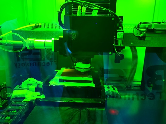
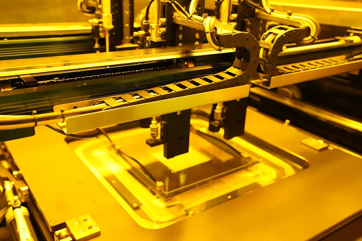
Precision and Technology
Manufacturing high-precision PCBs involves advanced machinery for etching, drilling, and plating. This machinery requires significant investment, and the skilled labor needed to operate it adds to the cost. The precision required in the production process ensures that the PCBs meet exacting standards, crucial for high-performance applications. A single advanced PCB drilling machine can cost upwards of $500,000.
Volume of Production
Smaller production runs generally have higher costs per unit because the setup and tooling expenses are spread over fewer units. For example, a low-volume production run of 10 PCBs might cost $100 per board, whereas a high-volume run of 10,000 boards might reduce the cost to $10 per board due to economies of scale.
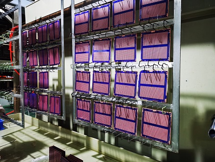
Testing and Quality Assurance
Rigorous testing, including electrical, thermal, and functional tests, ensures that the PCBs meet strict performance standards. This testing process is vital to ensure reliability, especially in critical applications like medical devices and aerospace. Quality assurance processes can add 20-30% to the overall production cost, but they are essential for maintaining high standards.
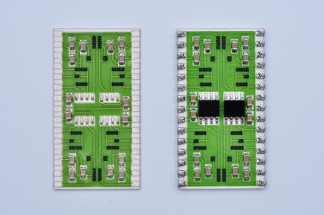
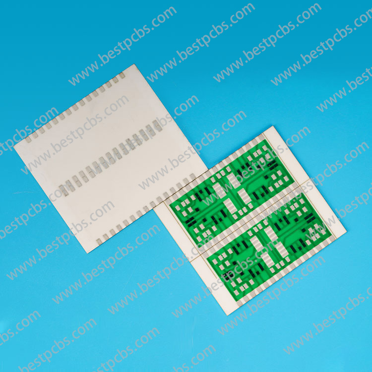
What is the Difference Between PCBA and PCB Board?
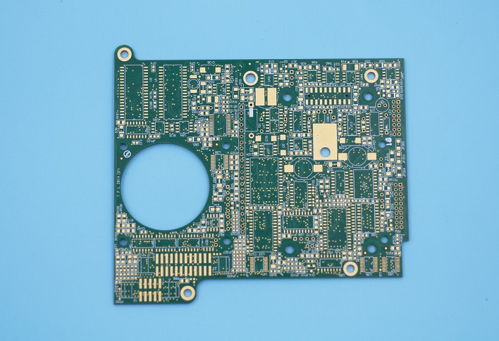
The terms PCB and PCBA are often used interchangeably, but they refer to different stages of the board’s life cycle. The PCB is the bare board itself, with no electronic components attached. It consists of a non-conductive substrate, copper traces, solder mask, and silkscreen. A PCB serves as the foundation for assembling electronic components.
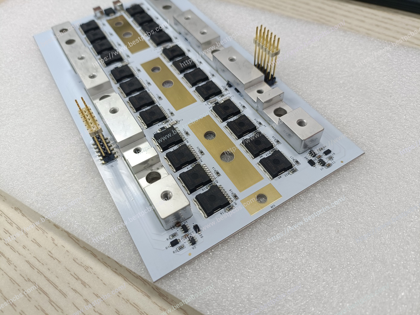
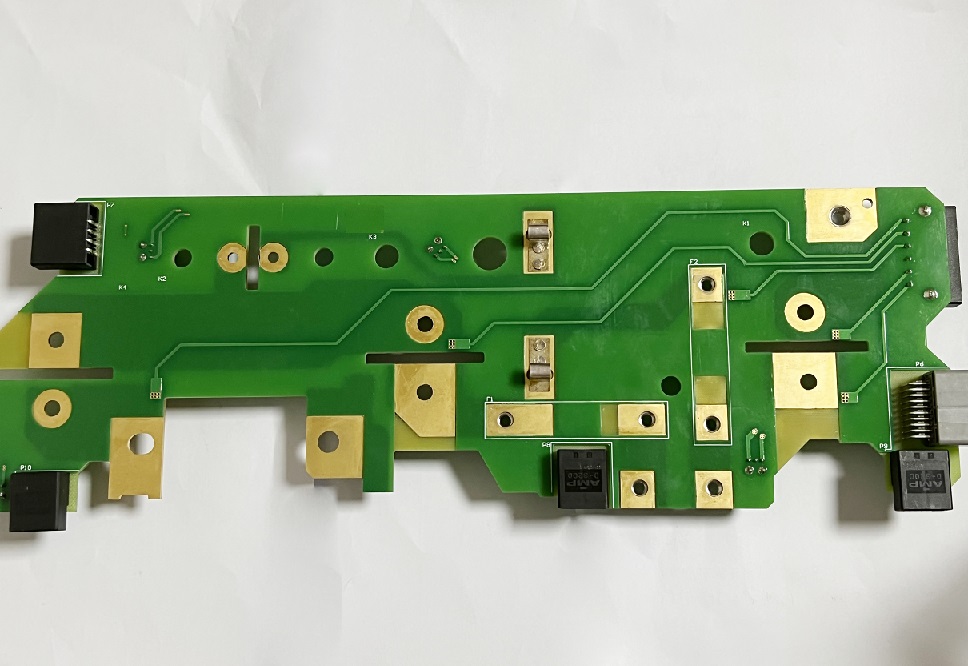
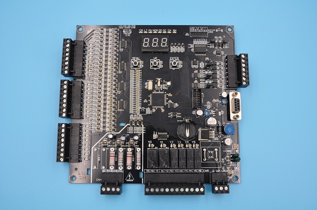
On the other hand, a PCBA (Printed Circuit Board Assembly) is a PCB that has undergone the assembly process, where all necessary electronic components like resistors, capacitors, diodes, and integrated circuits are soldered onto the board. Essentially, a PCBA is a functional circuit board ready for use in electronic devices. The transition from a PCB to a PCBA involves component placement, soldering, and quality testing, transforming the bare board into an operational assembly. Below is a typical PCBA product for your reference.
What is PCB Board Common Use?
PCB boards are existing in everywhere what we live, for example, the global smartphone market, which relies heavily on PCBs, was valued at approximately $520 billion in 2020. Here are some common applications that PCB used in:
Automotive Industry
In the automotive sector, PCBs are used in engine control units, infotainment systems, and advanced driver-assistance systems (ADAS). These applications enhance vehicle performance, safety, and connectivity.
Medical Devices
PCBs are integral to medical devices such as diagnostic equipment, patient monitoring systems, and implantable devices. They ensure precise and reliable operation, which is critical for patient safety and effective treatment.
Industrial Applications
PCBs are used in control systems, machinery, and power distribution units in industrial settings. They provide robust and durable solutions capable of withstanding harsh conditions and continuous operation.
Telecommunications
In telecommunications, PCBs are essential in routers, switches, and communication devices, ensuring efficient and reliable data transmission. As the demand for faster and more reliable communication networks grows, so does the need for high-quality PCBs.
Why Are Circuit Boards Green?
The characteristic green color of most PCBs comes from the solder mask, a protective layer applied over the copper traces to prevent oxidation, short-circuiting, and to protect the board during soldering.
The green color is traditional, largely due to historical reasons and practical benefits. Green solder mask provides a good contrast against the white silkscreen and the shiny copper traces, making it easier for technicians to inspect and identify components during assembly and troubleshooting. Additionally, green solder mask was one of the first colors to be developed and standardized in the industry, leading to its widespread adoption. However, PCBs are not limited to green; they can also be found in other colors such as red, blue, black, and white, depending on the specific requirements and aesthetic preferences of the project. The choice of solder mask color does not affect the performance of the PCB, but green remains popular due to its well-established manufacturing process and visual advantages.
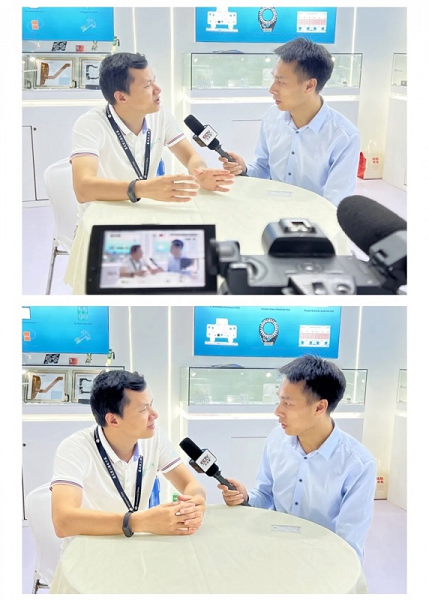
How to Get Started with EBest Circuit (Best Technology)?
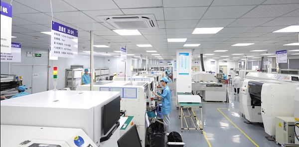
Here at EBest Circuit (Best Technology), we are experienced in designing all types of PCBs, including standard rigid PCBs, special PCBs, and irregular PCBs. We can design and develop PCBs according to customer specification and offer suggestions on the right materials for your project.
We provide the full series of PCB manufacturing, from the initial PCB design, PCB layout, to custom PCB fabricate, PCB assembly, box building and so forth. By the way, we have our own factory in Vietnam, that means we can ship out the PCBs directly from Vietnam.
Welcome to contact us when you want to get a quote!