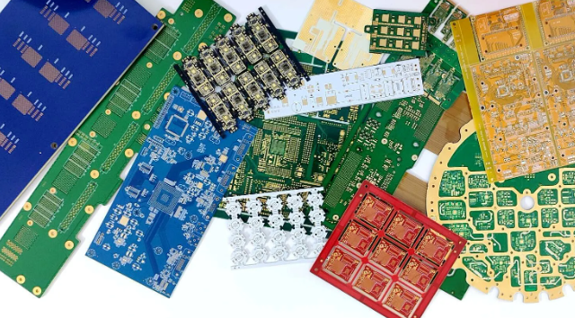
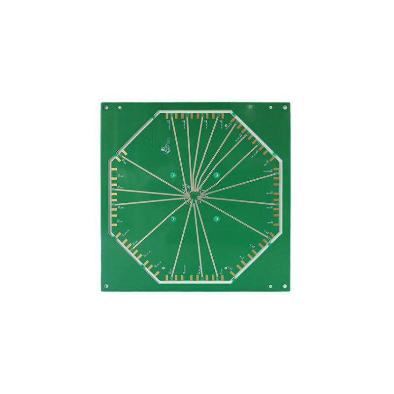
An empty circuit board is the starting point of almost every electronic product. Before chips, resistors, and connectors appear on a board, engineers begin with a bare platform that carries electrical pathways and mechanical structure. This base platform is the empty circuit board, also called a bare PCB.
EBest Circuit (Best Technology) has more than 19 years of PCB fabrication and assembly experience. Our engineering team supports projects from design review to final assembly. With integrated PCB fabrication and PCBA production, customers receive consistent quality, fast delivery, and practical engineering support throughout the process.
What Is an Empty Circuit Board?
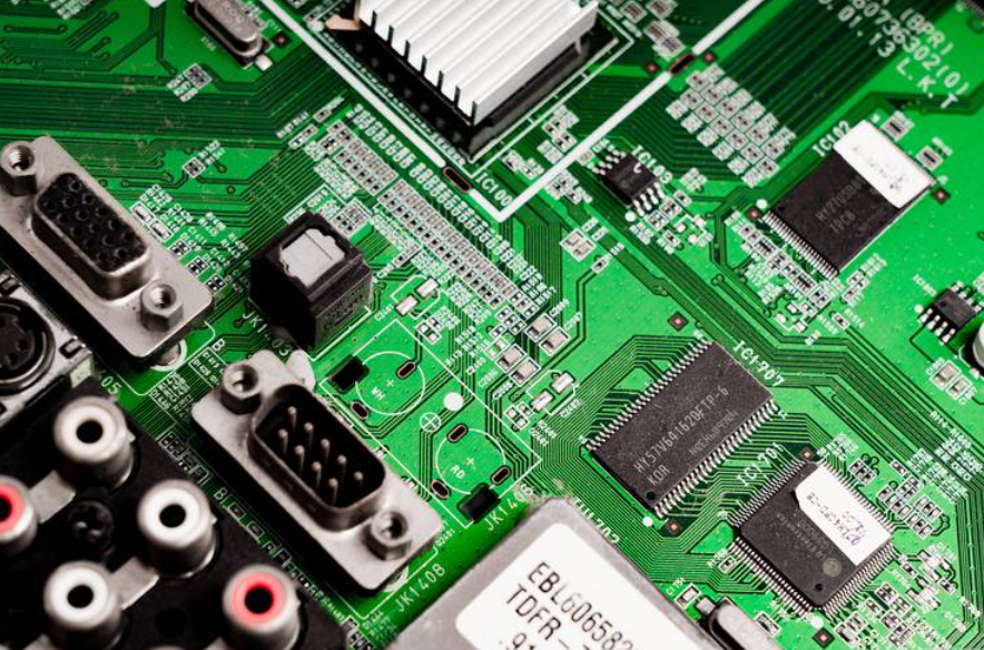
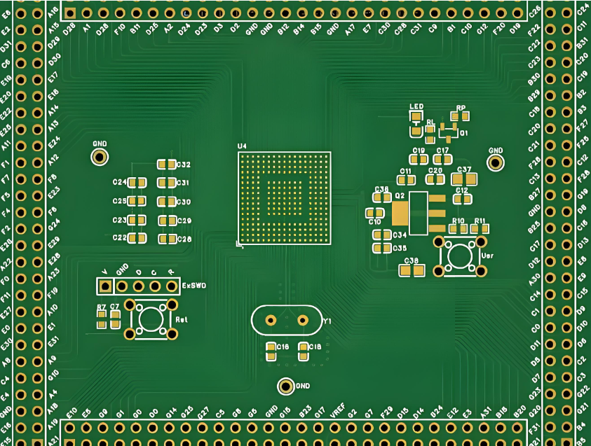
An empty circuit board refers to a printed circuit board before electronic components are mounted. It contains copper traces, vias, pads, and insulating substrate materials. These elements form the electrical network that later connects components.
In manufacturing terms, an empty circuit board is often called:
- Bare PCB
- Blank PCB
- Fabricated PCB
The board becomes a finished electronic module only after component assembly. That stage is known as PCBA (Printed Circuit Board Assembly).
What Materials Are Used in an Empty Circuit Board?
The materials inside an empty circuit board determine electrical performance and durability. Most boards combine insulating substrate materials with conductive copper layers.
1. Substrate Materials
The substrate forms the structural foundation of the PCB. Common substrate materials include:
- FR4 fiberglass epoxy – the most widely used PCB material
- High-TG FR4 – suitable for higher thermal environments
- Polyimide – used for flexible circuits
- Aluminum core – used for heat dissipation
- Ceramic materials – used in high-frequency electronics
Among these options, FR4 remains the standard choice because it balances cost, strength, and electrical insulation.
2. Copper Layers
Copper forms the conductive pathways on the board. These traces connect electronic components. Copper thickness is measured in ounces (OZ) per square foot. Typical copper thickness values include:
| Copper Weight | Thickness | Application |
| 0.5 oz | ~17 µm | Fine-line circuits |
| 1 oz | ~35 µm | Standard electronics |
| 2 oz | ~70 µm | Power electronics |
| 3 oz+ | 100 µm+ | High-current circuits |
Higher copper thickness improves current capacity and thermal performance.
3. Solder Mask
Solder mask is the colored protective layer on top of the PCB. It prevents solder bridging during assembly. Common colors include:
- Green
- Black
- Blue
- White
- Red
Green remains the most common color because it offers good contrast for inspection.
4. Surface Finish
The copper pads require protective coating. Surface finishes prevent oxidation and improve solderability. Typical finishes include:
- HASL (Hot Air Solder Leveling)
- ENIG (Electroless Nickel Immersion Gold)
- ENEPIG
- Immersion silver
- OSP coating
Each finish has advantages depending on product requirements.
How Is an Empty Circuit Board Manufactured?
Manufacturing an empty circuit board involves multiple precision processes. Each step builds part of the board structure. Below is a simplified overview of the process.
1. Design File Preparation
Engineers prepare design files using PCB design software. These files define trace routing, drill holes, and board dimensions. Typical design files include:
- Gerber files
- Drill files
- Stack-up specifications
2. Material Preparation
3. Inner Layer Imaging
4. Etching
5. Lamination
6. Drilling
7. Copper Plating
8. Solder Mask Application
9. Surface Finish
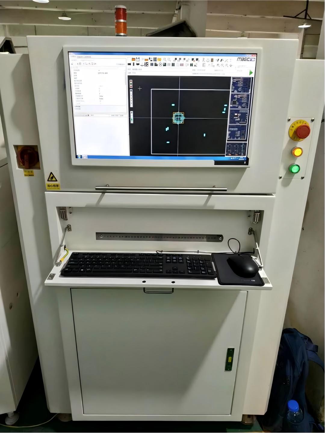
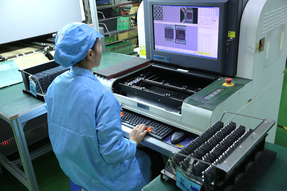
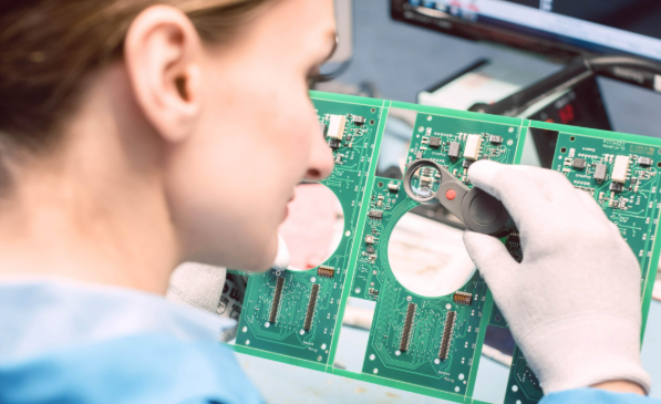
10. Electrical Testing
If you want to know more the manufacturing process of empty circuit board, you can watch below video from our PCB fabrication workshop:
What Are the Different Types of Empty Circuit Boards?
Empty circuit boards are not all built the same. Engineers select different PCB structures based on circuit complexity, signal speed, thermal conditions, and mechanical requirements. Below are the most common types of empty circuit boards used in modern electronics manufacturing.
1. Single-Layer Empty Circuit Board
A single-layer circuit board contains one conductive copper layer on one side of the substrate. All components and traces appear on the same surface.
Typical applications include:
- LED lighting modules
- Power adapters
- Small household electronics
- Simple control boards
However, routing space is limited because all connections must exist on one layer.
2. Double-Layer Empty Circuit Board
A double-layer circuit board contains copper layers on both the top and bottom surfaces of the substrate. Electrical connections between the two layers are created using plated through holes (vias).
Double-layer PCBs are widely used in:
- consumer electronics
- industrial control systems
- communication devices
- embedded modules
Because they provide more routing space than single-layer boards, they remain a practical solution for medium-complexity designs.
3. Multilayer Empty Circuit Board
A multilayer PCB contains three or more copper layers stacked together through lamination. Some advanced boards may include 8, 12, or even more layers.
Common applications include:
- smartphones and tablets
- computer motherboards
- networking equipment
- high-speed communication systems
Although multilayer PCBs require more manufacturing steps, they enable compact designs and higher performance.
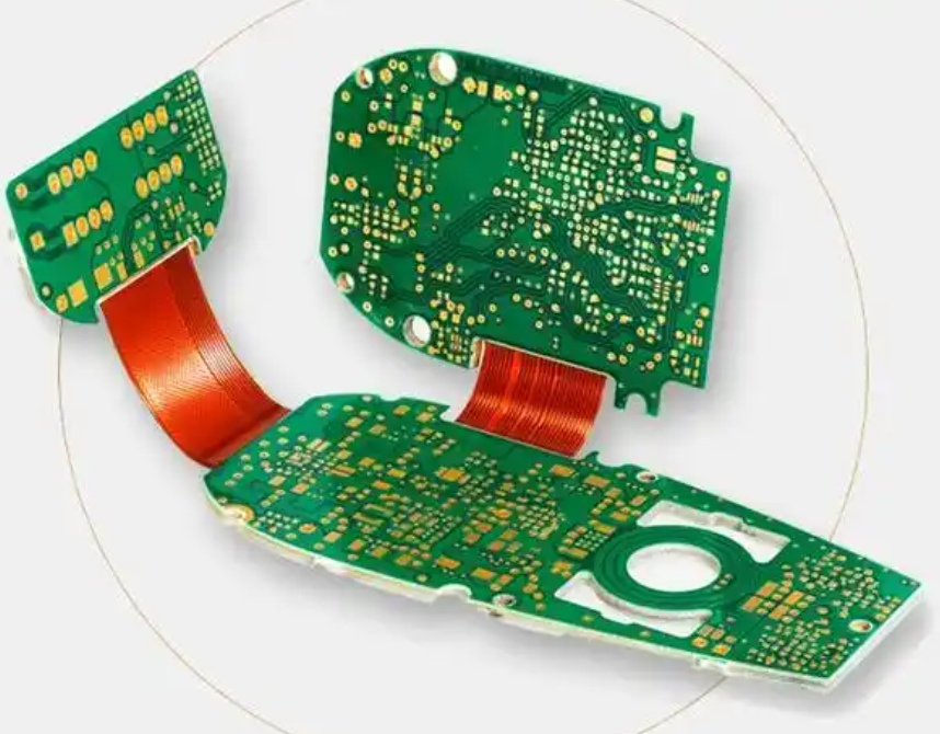
4. Flexible Circuit Boards
A flexible PCB uses polyimide or similar flexible substrate materials instead of rigid fiberglass. The board can bend, twist, or fold without damaging the circuit. Flexible boards reduce connector usage and improve space utilization in compact devices.
Typical applications include:
- wearable electronics
- camera modules
- medical instruments
- portable consumer devices
5. Rigid-Flex Circuit Boards
A rigid-flex PCB combines rigid circuit board sections with flexible interconnections in a single structure.
Rigid-flex boards are often used in:
- aerospace electronics
- medical equipment
- military systems
- advanced communication devices
Although the design and manufacturing process are more complex, rigid-flex PCBs offer excellent durability and compact integration.
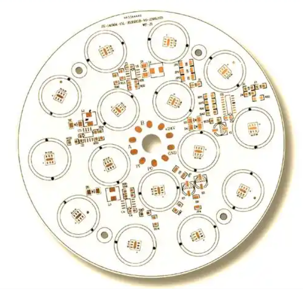
6. Metal Core Circuit Boards
A metal core PCB (MCPCB) uses a metal base layer, usually aluminum or copper, instead of standard fiberglass. Metal core boards are widely used in:
- high-power LED lighting
- automotive lighting systems
- power converters
- industrial power modules
Because thermal performance is critical in these applications, metal core boards provide a reliable solution.
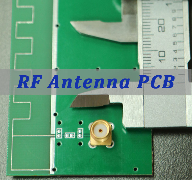
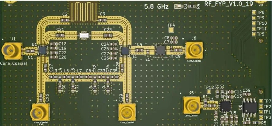
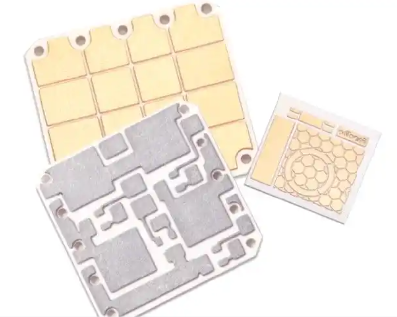
7. Ceramic Circuit Board
A ceramic PCB uses ceramic materials such as aluminum oxide (Al₂O₃) or aluminum nitride (AlN) as the substrate instead of fiberglass. Ceramic materials provide excellent thermal conductivity, electrical insulation, and dimensional stability.
Key advantages include:
- excellent heat dissipation
- high electrical insulation strength
- stable performance at high temperatures
- low signal loss at high frequencies
Ceramic PCBs are widely used in:
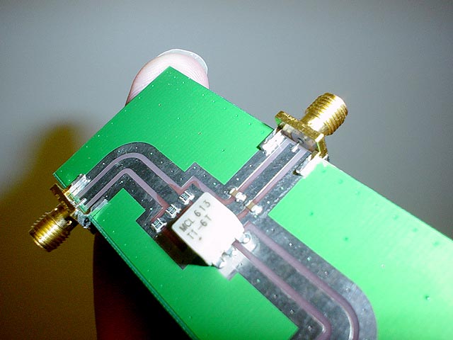
- RF communication modules
- power semiconductor modules
- laser equipment
- automotive electronics
- aerospace electronics
Although ceramic boards are more expensive than standard FR4 PCBs, they deliver superior performance in demanding environments.
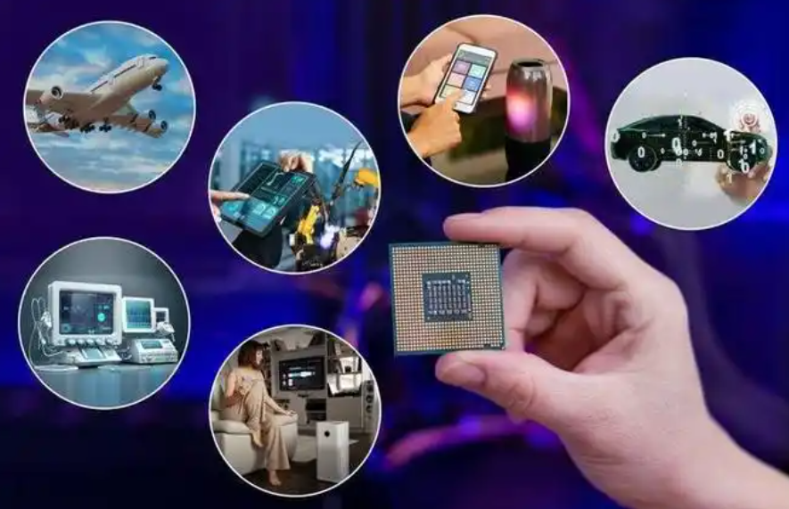
Where Are Empty Circuit Boards Used?
Empty circuit boards serve as the base platform for almost all electronic products. Before components are mounted, the board provides routing paths, grounding structures, and mechanical support for the final system.
Common applications include:
- Consumer electronics – smartphones, smart home devices, wireless earbuds, and wearable gadgets
- Computer hardware – motherboards, graphics cards, memory modules, and storage controllers
- Automotive – engine control units, battery management systems, infotainment modules, and sensor interfaces
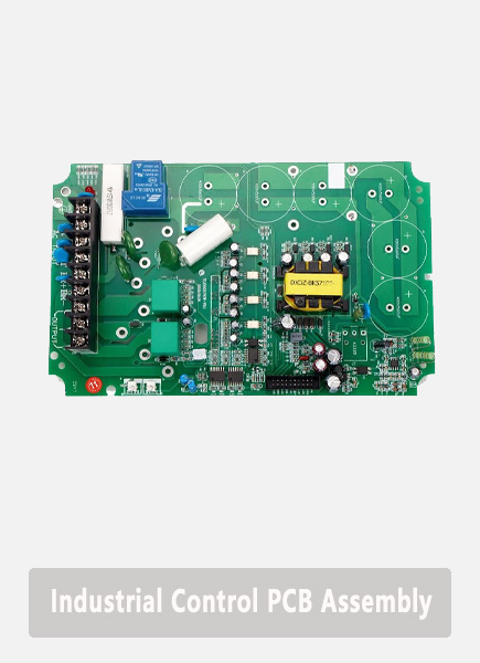
- Industrial automation systems – PLC controllers, motor drivers, robotics control boards, and industrial power supplies
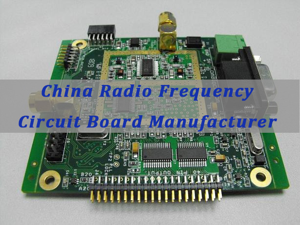
- Communication equipment – routers, base stations, RF communication modules, and network switches
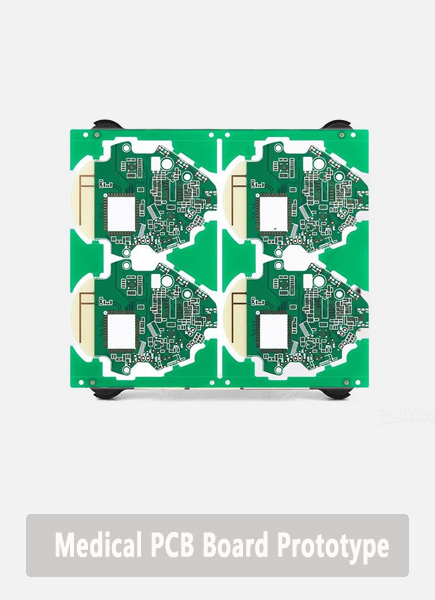
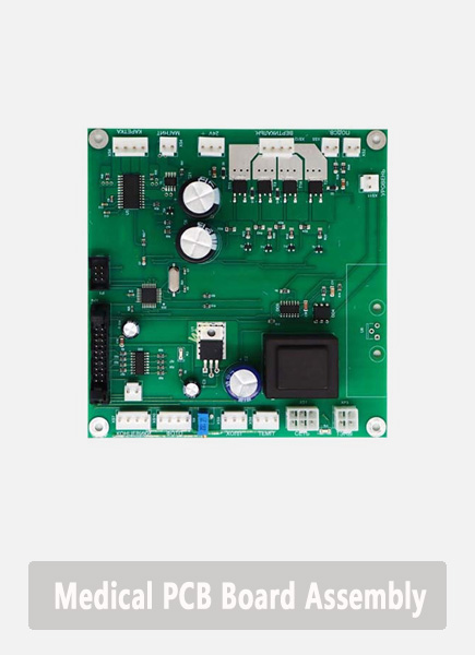
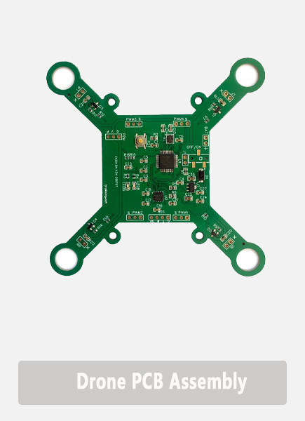
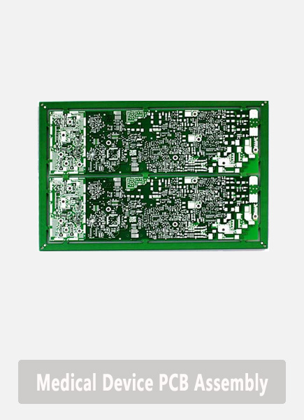
- Medical devices – patient monitoring systems, diagnostic equipment, imaging systems, and portable healthcare electronics
- LED lighting systems – commercial lighting, automotive lighting, and architectural illumination.
How Much Does an Empty Circuit Board Cost?
The cost of an empty circuit board varies widely. Several factors influence manufacturing price, major cost factors including:
1. Board size
2. Layer count
3. Material type
4. Copper thickness
5. Surface treatment
6. Production quantity
Here is a general cost for empty circuit boards:
| PCB Type | Typical Cost Range |
| Single layer | $1 – $5 |
| Double layer | $3 – $15 |
| Multilayer PCB | $20 – $200+ |
These values vary depending on complexity and quantity. Working with an experienced manufacturer helps control cost while maintaining quality.
Empty Circuit Board vs Assembled PCB
An empty circuit board and an assembled PCB represent two different stages in electronic manufacturing. The empty board provides the physical and electrical platform. The assembled PCB transforms that platform into a working electronic module. Below is comparison chart between them:
| Item | Empty Circuit Board (Bare PCB) | Assembled PCB (PCBA) |
| Definition | PCB structure without electronic components | PCB with components soldered and fully functional |
| Manufacturing Stage | PCB fabrication | PCB assembly |
| Main Processes | Lamination, drilling, plating, etching, solder mask, surface finish | SMT placement, reflow soldering, wave soldering, inspection |
| Electrical Function | Provides conductive pathways but no active functionality | Fully operational circuit |
| Components Installed | None | Resistors, capacitors, ICs, connectors, sensors |
| Typical Layer Count | 1–20+ layers depending on design | Same as PCB but populated with parts |
| Manufacturing Time | Usually 3–7 days for prototypes | 5–10 days depending on component sourcing |
| Testing Method | Electrical continuity test | Functional test, AOI, X-ray inspection |
| Cost Structure | Mostly determined by material, layer count, board size | Includes PCB cost, components, assembly labor |
| Weight | Very light since no components are installed | Heavier due to electronic parts |
| Application Stage | Used during early design, testing, and prototyping | Used in final electronic products |
| Production Complexity | Medium complexity fabrication | Higher complexity due to placement accuracy |
| Typical Use | Engineering validation and prototyping | Consumer electronics, industrial equipment, automotive electronics |
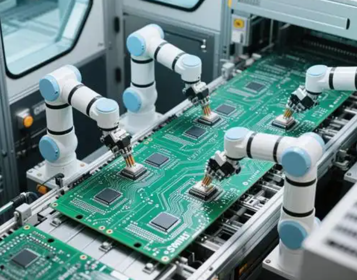
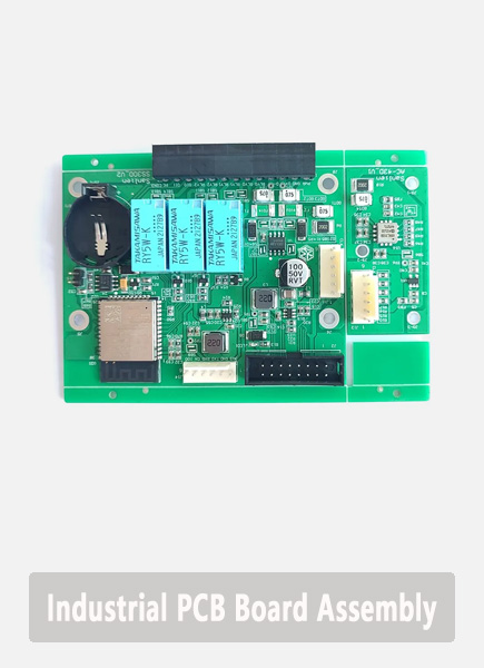
From a manufacturing perspective, the empty circuit board acts as the foundation of the electronic system. Once components are installed through SMT or THT assembly processes, the board becomes a functional PCBA ready for integration into a product.
Why Choose EBest as Your Empty Circuit Board & Assembled PCB Manufacturer?
Best Technology (EBest Circuit) is a PCB and PCBA manufacturer with 19 years of industry experience, headquartered in Shenzhen, one of the world’s most important electronics manufacturing hubs. To better support global customers and ensure flexible supply chains, we have established production facilities in both China and Vietnam, allowing us to provide stable manufacturing capacity and competitive lead times.
Our advantages include:
- 19 Years of PCB & PCBA Manufacturing Experience
- Professional R&D and engineering team
- 1+3 engineering support model
- One-stop PCB Fabrication and PCBA Assembly
- Rapid prototype and production turnaround
- Full Digital Manufacturing System
- No MOQ, flexible order quantities
- Global customer support experience across North America, Europe, and Asia
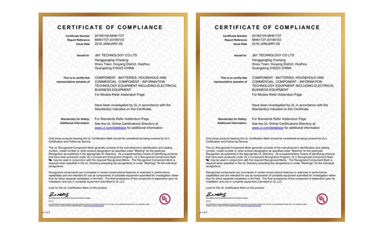
- ISO 9001, ISO 13485, IATF 16949, and AS9100D certificated
If you are planning a new electronics project or looking for a dependable PCB manufacturing partner, feel free to contact our engineering team.
We are always ready to support your next circuit board project.
FAQs
1. Is an empty circuit board the same as a PCB?
Yes. An empty circuit board is commonly called a bare PCB. It includes copper traces and pads but no electronic components.
2. What thickness do empty PCBs usually have?
Typical PCB thickness ranges from 0.8 mm to 1.6 mm. Thinner boards exist for compact electronics, while thicker boards provide higher mechanical strength.
3. What files are required to manufacture a PCB?
Manufacturers usually require the following files:
- Gerber files
- Drill files
- PCB stack-up information
- Bill of materials (for assembly)
These files define the complete board structure.