What Is copper plating PCB? Let’s discover its meaning, benefits, application, plating methods and process through this blog.
Are you worried about these issues?
- How to solve the problem of uniformity of thick copper plate coating?
- How to control the plating defects in the copper deposition process?
- Can the plating cycle of high-layer boards be shortened?
EBest Circuit (Best Technology) Can Provide:
- Use pulse plating + intelligent temperature control system to achieve ≥95% plating uniformity.
- Patented chemical solution formula, plating rate is less than 0.5ppm.
- Vertical continuous plating production line, delivery time shortened by 30%.
Welcome to contact us if you have any request for PCB: sales@bestpcbs.com.
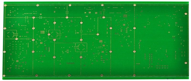
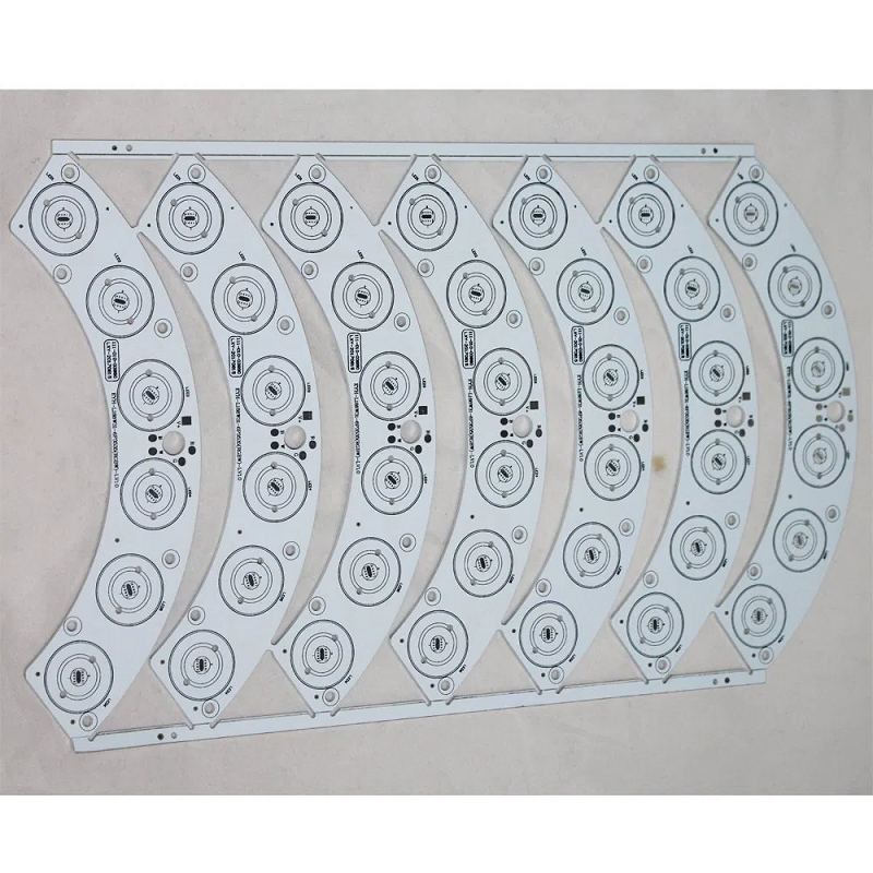
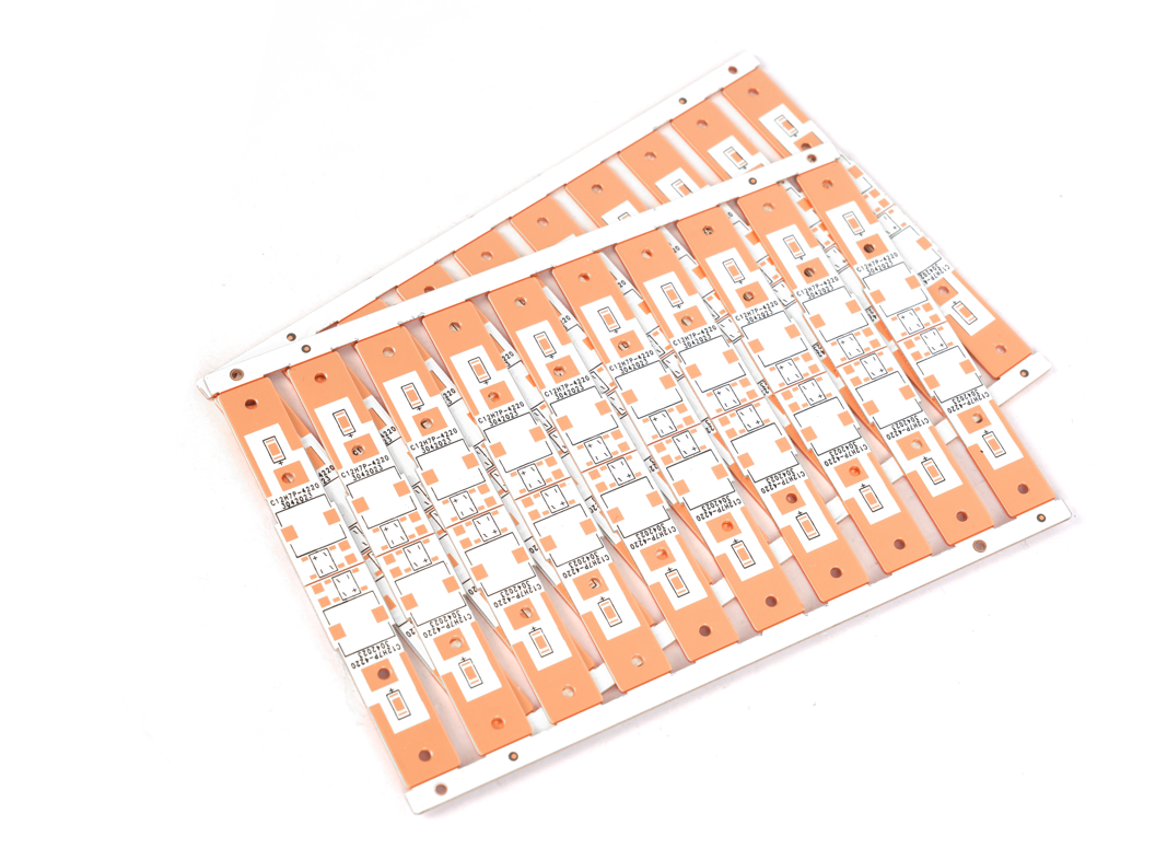
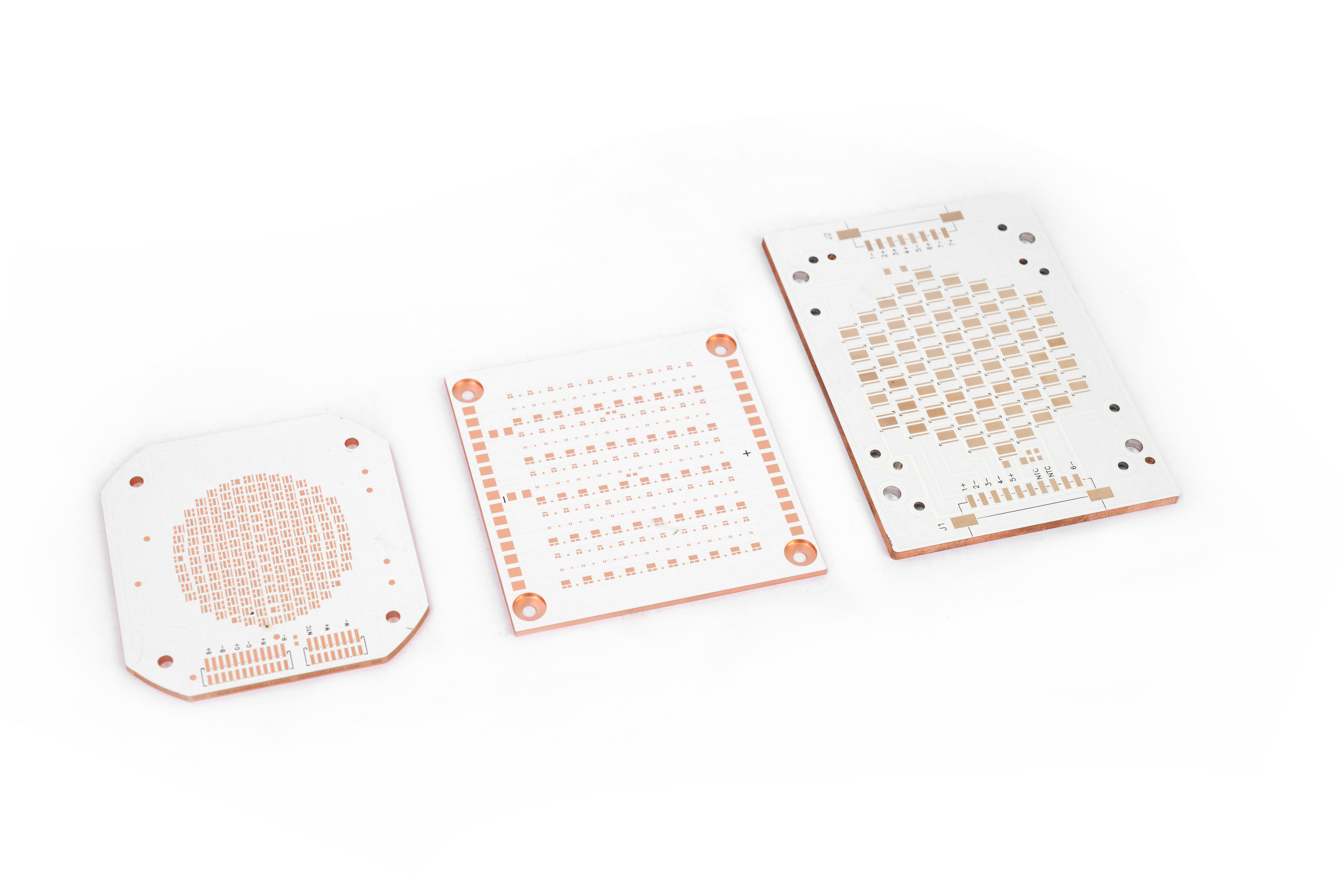
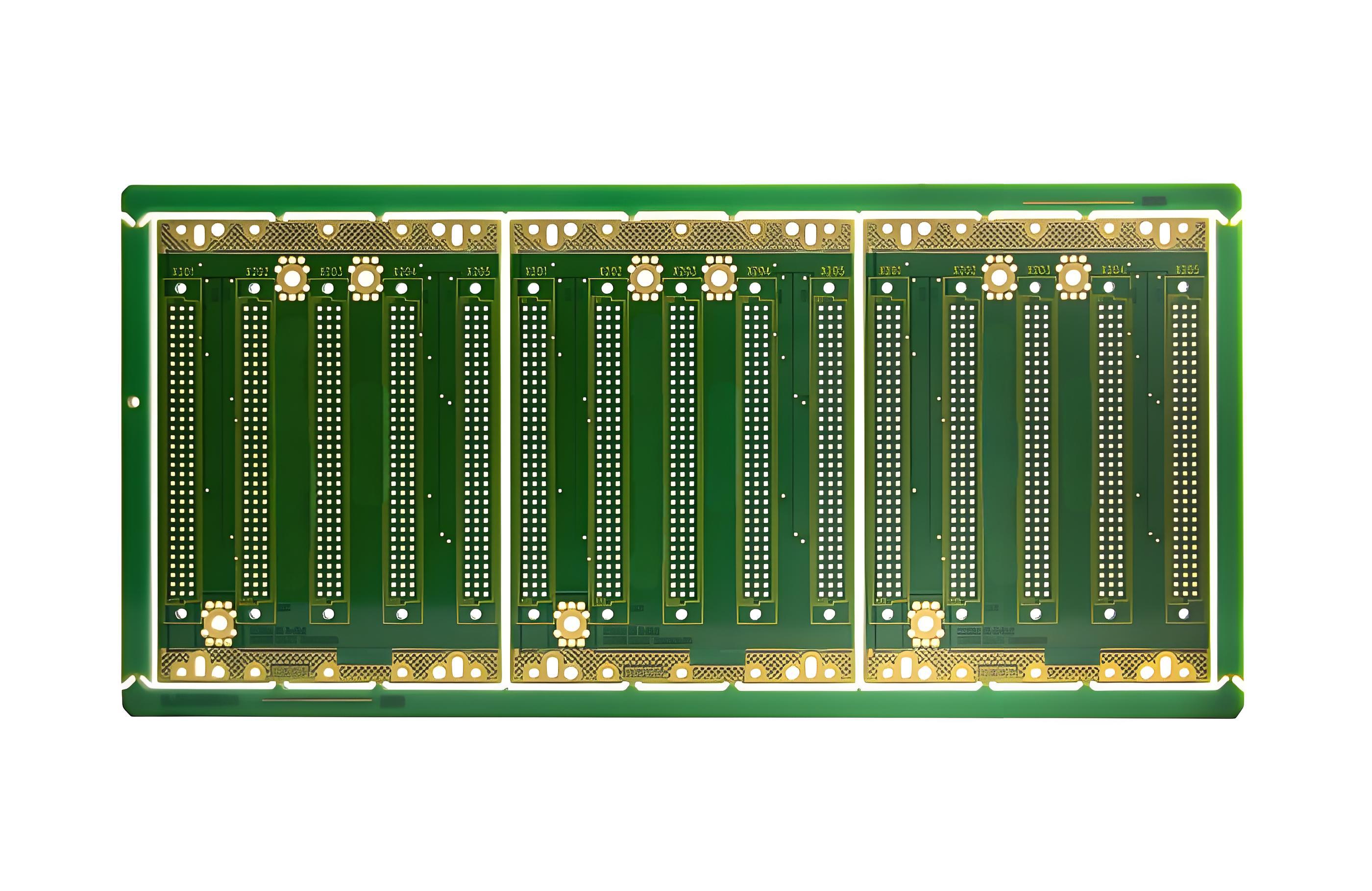
What Is Copper Plating PCB?
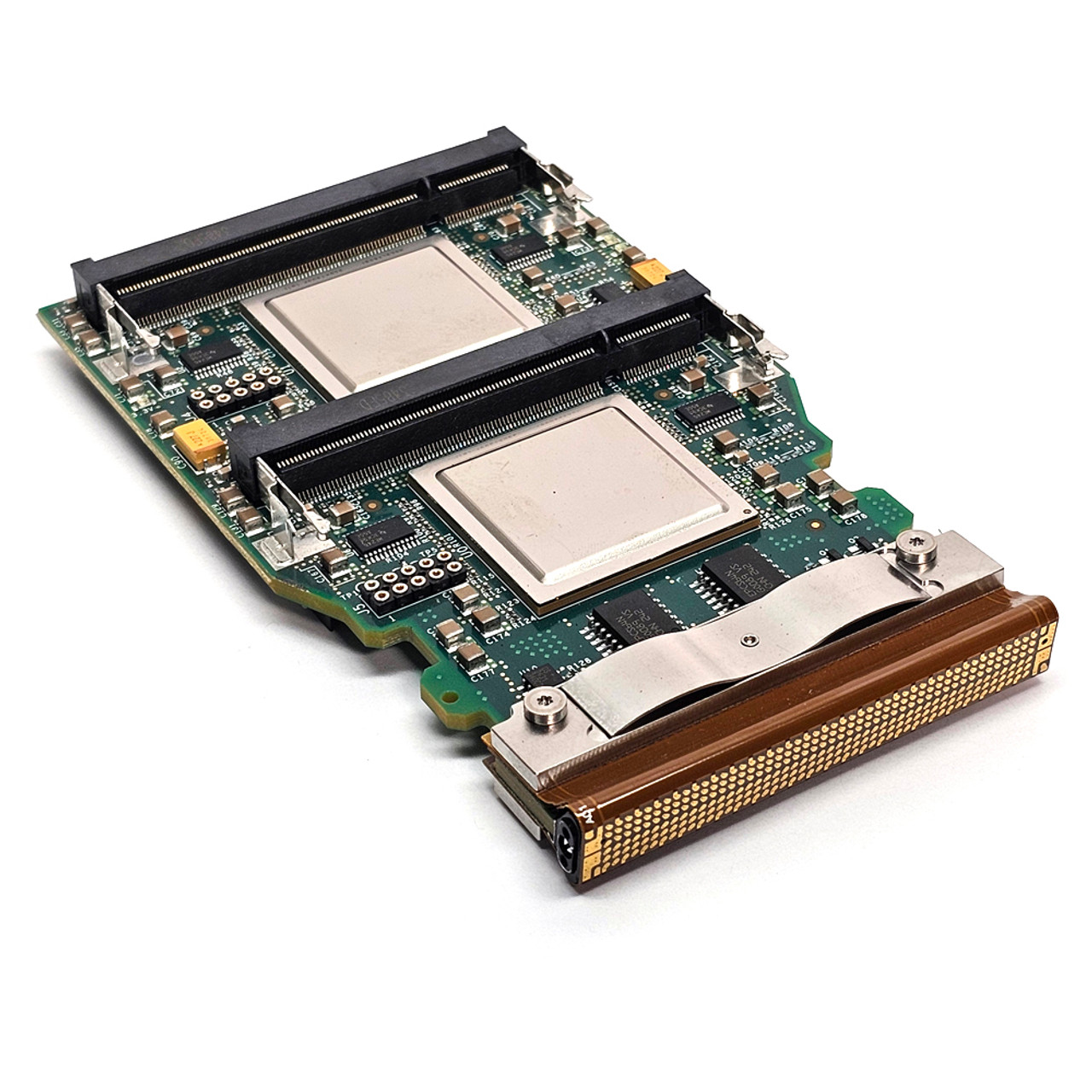
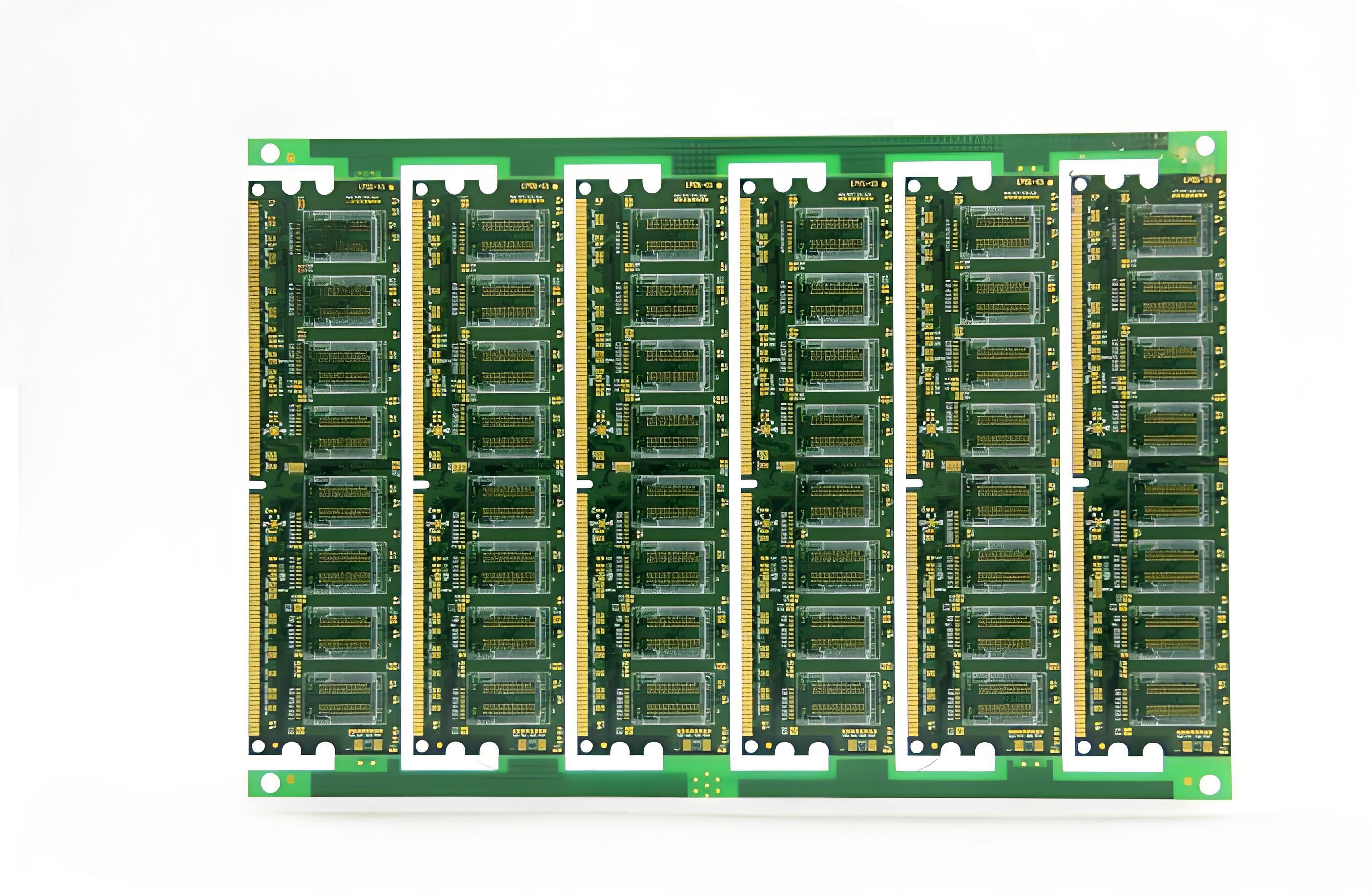
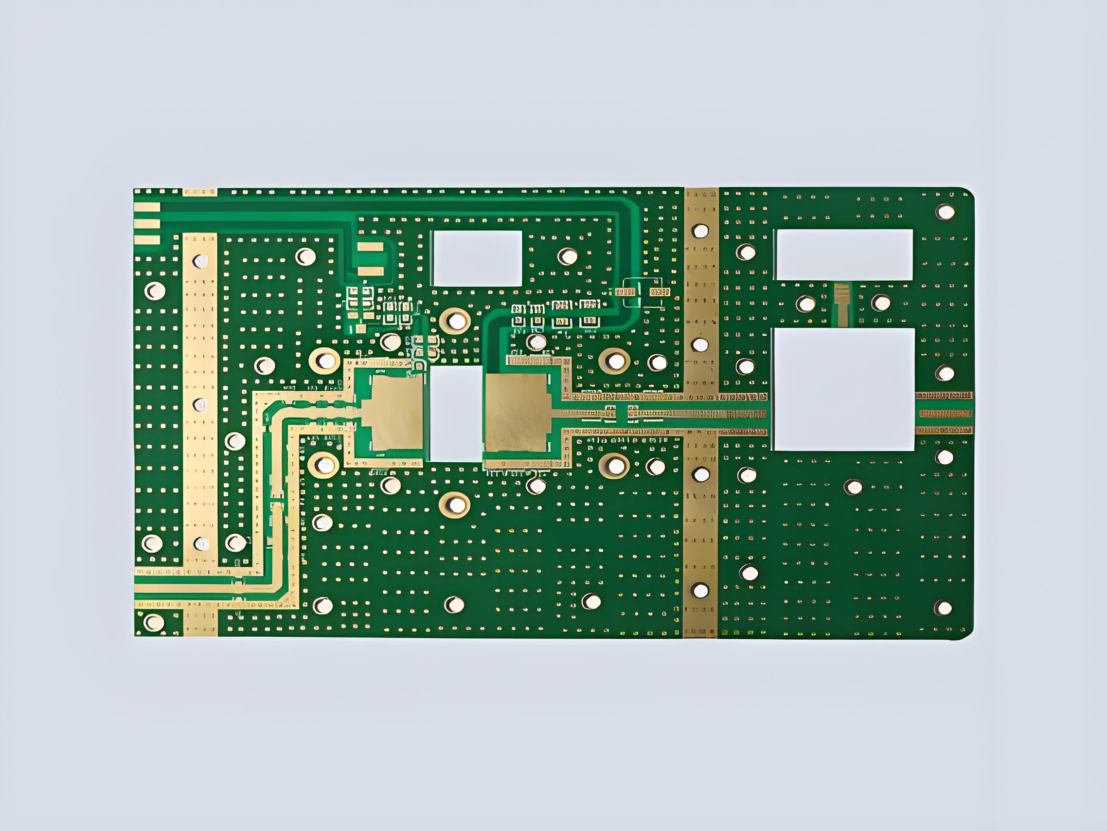
Copper plating in PCB manufacturing creates conductive pathways by electrochemically depositing copper onto substrate surfaces. The process uses acid-copper sulfate solutions where direct current reduces copper ions into metallic form, building layers typically 0.5-3 mils thick for reliable current conduction.
Modern techniques employ pulse-reverse current to achieve uniform deposition, especially in high-aspect-ratio vias, preventing defects while maintaining consistent thickness. The plating bath contains organic additives that refine copper grain structure to 0.2-0.8μm, improving conductivity and mechanical durability. Process parameters like current density (15-35 ASF), temperature (20-28°C), and copper concentration (40-60 g/L) are tightly controlled to meet industry standards for signal integrity and thermal reliability.
Advantages of Copper Plating PCB
- Enhanced Conductivity: Copper purity exceeds 99.9%, reducing impedance by 15% compared to rolled copper foils for high-frequency signals (>10 GHz).
- Structural Coverage Capability: Pulse plating achieves uniform ≥1μm coatings in through-holes, eliminating copper void defects.
- Cost Efficiency: Enables ultra-thin 3-5μm conductive layers, cutting raw material costs by 20% versus foil lamination.
- Thermal Management: Peel strength >1.5 N/mm with 30% improved CTE matching minimizes delamination at high temperatures.
- Design Flexibility: Supports 50μm fine-line circuitry, increasing routing density by 40% over traditional etching.
- Environmental Compliance: Cyanide-free process meets RoHS 3.0 standards, reducing wastewater treatment costs by 35%.
- Repairability: Re-plating capability cuts repair expenses to 1/5 of foil replacement costs.
Applications of Copper Plating PCB Board
- High-Frequency Circuits – Enables stable signal transmission up to 40GHz for 5G/WiFi-6E applications due to ultra-smooth surface finish (Ra<0.3μm).
- Power Electronics – Supports 20A/mm² current density in automotive/industrial PCBs through customizable thickness (30-300μm).
- Miniaturized Devices – Allows 0.1mm micro-via filling for wearables/medical implants using bottom-up electroplating technology.
- Thermal-Critical Systems – Provides 3D heat dissipation paths in LED/CPU substrates with 95% via-filling rate.
- Flexible Electronics – Maintains conductivity after 100,000 bending cycles (r=3mm) for foldable displays.
- High-Reliability Products – Eliminates CAF (conductive anodic filament) failure in aerospace/military PCBs through void-free plating.
- Cost-Sensitive Applications – Reduces gold usage by 70% in edge connectors via selective copper-nickel-gold stacking.
- High-Density Interconnects – Enables 15μm line/space in chip packaging substrates with additive plating process.
- Harsh Environment Use – Withstands 1000hrs salt spray testing for marine/outdoor equipment applications.
- RF Shielding – Creates seamless EMI cages around components through conformal cavity plating.
PCB Copper Plating Methods
Below are methods about PCB copper plating:
- Pulse Plating – Enables 10:1 aspect ratio via filling with ±1μm thickness uniformity, reducing blind via void risk by 50%.
- Direct Metallization – Eliminates electroless copper step, cutting process time 40% and wastewater treatment costs 60%.
- Horizontal Plating – Processes ultra-thin 18μm substrates with ±0.3μm thickness tolerance, compatible with roll-to-roll production.
- Selective Plating – Achieves localized 100μm thickness, reducing gold usage 70% for high-wear connectors.
- Via Filling Plating – Ensures 100% void-free filling, improving thermal cycling performance 3x (MIL-STD-202G).
- Electroless Copper – Covers 3D irregular structures at 8μm/h deposition rate, adhesion >1.2kN/m.
- Pattern Plating – Forms 15μm fine traces with <5μm undercut, increasing routing density 30%.
- Through-Hole Plating – Maintains ≥25μm copper thickness in 10:1 aspect ratio holes (IPC-6012 Class 3 compliant).
- Masked Plating – Controls regional thickness variation within ±5%, reducing etchant consumption 35%.
- High-Speed Plating – Operates at 10μm/min deposition rate, boosting productivity 5x for mass production.
PCB Copper Plating Process
1. Surface Preparation
- Microetching: Creates 1-3μm roughness for optimal adhesion (180° peel strength >8N/cm)
- Degreasing: Removes organic contaminants with <0.1mg/cm² residue
2. Catalyst Application
- Palladium Activation: Deposits 0.02-0.05μm catalytic layer for uniform initiation
3. Electroless Copper Deposition
- Autocatalytic Process: Builds 0.3-1μm seed layer at 15-25°C (deposition rate 4-6μm/hr)
4. Electrolytic Plating
- DC Plating: Standard 20-40μm build-up (current density 2-3ASD)
- Pulse Plating: For HDI boards (aspect ratio >8:1, thickness deviation ±5%)
5. Via Filling Technology
- Reverse Pulse: Achieves void-free filling in ≤100μm microvias (fill time <60min)
6. Post-Treatment
- Anti-Tarnish: Organic coating prevents oxidation (salt spray resistance >96hrs)
- Annealing: 180°C heat treatment improves ductility (elongation >15%)
7. Quality Control
- Cross-Section Analysis: Measures thickness uniformity (IPC-6012 Class 3 compliant)
- Pull Testing: Verifies >1kN via barrel strength
8. Waste Management
- Closed-Loop System: Recovers >95% copper from drag-out solutions
- Each step includes measurable parameters directly impacting yield, reliability, and cost-efficiency.
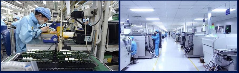
Why Choose EBest Circuit (Best Technology) as Copper Plating PCB Manufacturer?
Reasons why choose EBest Circuit (Best Technology) as copper plating PCB manufacturer:
- Various Surface Finishes: Support mixed finishes (like ENIG+OSP on one board) to reduce cost by 15-40%
- 24-hour rapid prototyping: shorten the R&D cycle by 50% and accelerate product launch
- 1 Piece MOQ: zero inventory risk, trial production cost reduced by 90%
- Competitive & Transparent Pricing – No hidden costs, offering the best value without compromising quality.
- Turnkey Solutions – Full-service PCB manufacturing from design to delivery, accelerating your product’s time-to-market.
- ISO 14001/ISO 13485 certification: medical/automotive customers are exempt from secondary testing, and compliance costs are reduced by 30%
- Free DFM (Design for Manufacturability) Analysis: Optimizes PCB layouts to reduce material waste, lower production costs, and avoid late-stage design revisions.
Our Available Surface Treatment Types
Hot Air Solder Leveling (HASL)
- Types: Lead-free (environmentally friendly), Lead-containing (traditional).
- Features: Low cost, excellent solderability, suitable for PCBs with wide component spacing.
- Limitations: Poor surface flatness, not suitable for high-density fine-pitch components.
Organic Solderability Preservative (OSP)
- Principle: Forms an organic protective film on copper surfaces to prevent oxidation; environmentally friendly.
- Advantages: Simple process, low cost, high surface flatness.
- Applications: High-frequency signal transmission and lead-free soldering scenarios.
Electroless Nickel Immersion Gold (ENIG)
- Structure: Nickel layer (3-6μm) + Gold layer (0.05-0.15μm).
- Advantages: Excellent flatness, strong corrosion resistance, ideal for high-end products (e.g., BGAs, smartphone motherboards).
- Risks: Potential “black pad” phenomenon (nickel layer corrosion) requiring process control.
Immersion Silver
- Characteristics: Surface roughness <0.12μm, suitable for high-frequency signals (5G/mmWave).
- Advantages: Excellent conductivity, fast processing, cost-effective.
- Note: Requires sulfurization prevention and storage environment control.
Immersion Tin
- Advantages: Wide soldering compatibility, lead-free, flat surface.
- Limitations: Short storage life (typically ≤6 months), tin whisker control needed.
Hard Gold Plating
- Applications: High-wear scenarios (e.g., gold fingers, connectors).
- Properties: Gold thickness ≥0.3μm, withstands >10,000 insertion cycles.
- Process: Requires nickel underplating to prevent diffusion.
Electroless Nickel Electroless Palladium Immersion Gold (ENEPIG)
- Structure: Nickel + Palladium + Gold triple layer, eliminates ENIG black pad defects.
- Advantages: Strong thermal stability, suitable for multiple reflows and chip packaging.
How to Get A Quote for Your PCB Project?
PCB Specification Requirements
1. Base Material Details
- Board type (FR-4, high-frequency, flexible, etc.)
- Thickness requirements (standard 1.6mm or specific)
- Copper weight (e.g., 1oz, 2oz)
2. Design Parameters
- Quantity requirements (prototype/bulk)
- Board dimensions (max/min size)
- Layer count (single/double/multi-layer)
- Minimum trace/space width
- Hole specifications (plated/non-plated, sizes)
3. Surface Treatment Selection (Reference our available options)
- Preferred finish type
- Special requirements (e.g., ENIG with >5μm nickel)
- Edge connector treatment if applicable
4. Special Processes
- Impedance control requirements
- Via treatment (tented, plugged, etc.)
- Silkscreen/legend color
- Solder mask color and type
5. Testing & Certification
- Electrical testing needs (flying probe, AOI)
- IPC Class requirements
- Special certifications (UL, RoHS, etc.)
6. Delivery Requirements
- Target delivery date
- Packaging specifications
- Shipping destination
7. Additional Documentation (Attach if available)
- Gerber files (RS-274X preferred)
- Drill files
- Stack-up diagram
- Special instructions document
Welcome to contact EBest Circuit (Best Technology) to get a free quote for your PCB project: sales@bestpcbs.com.