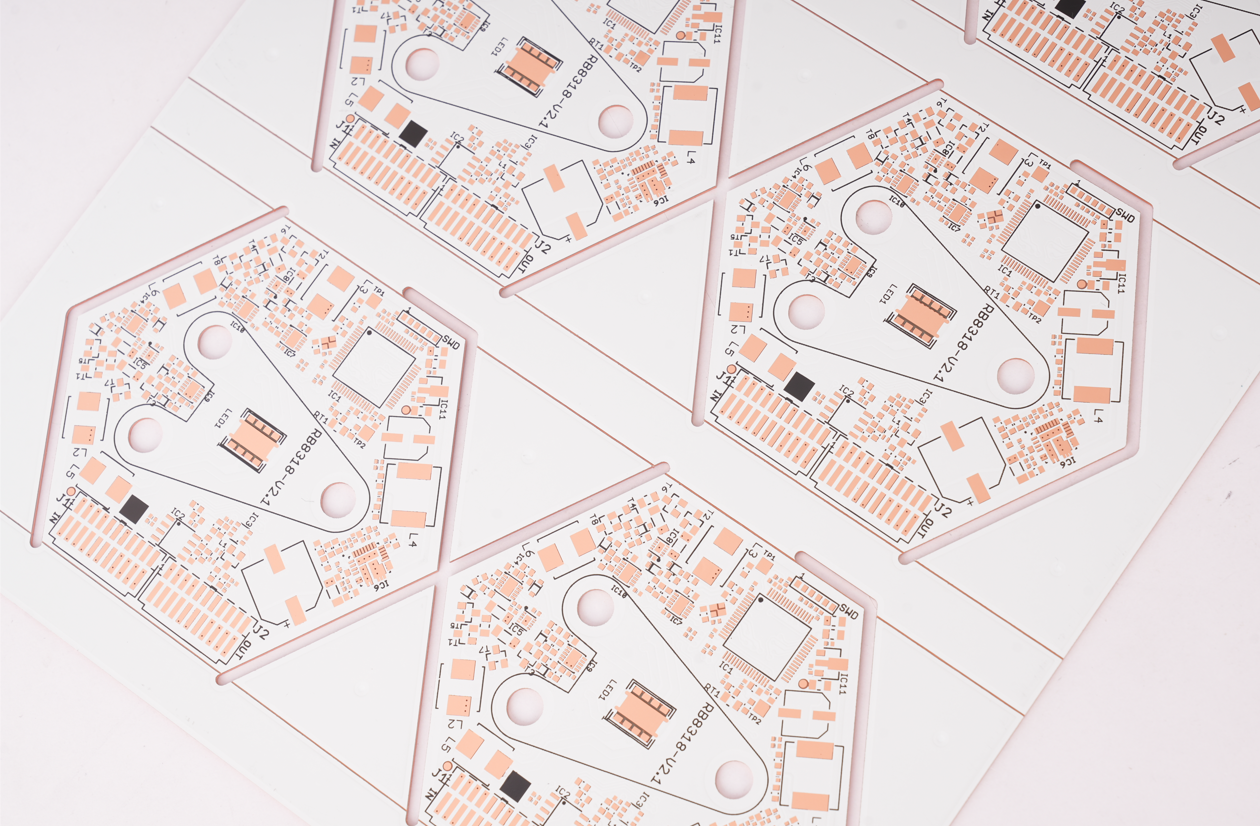
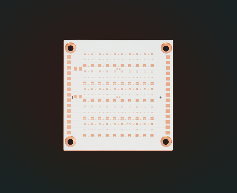
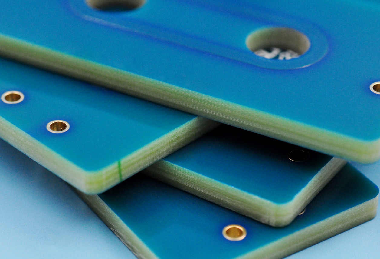
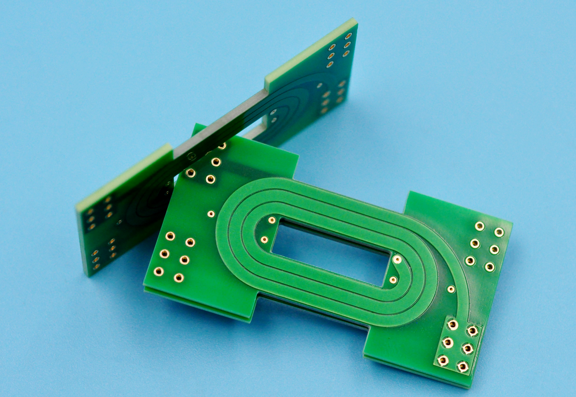
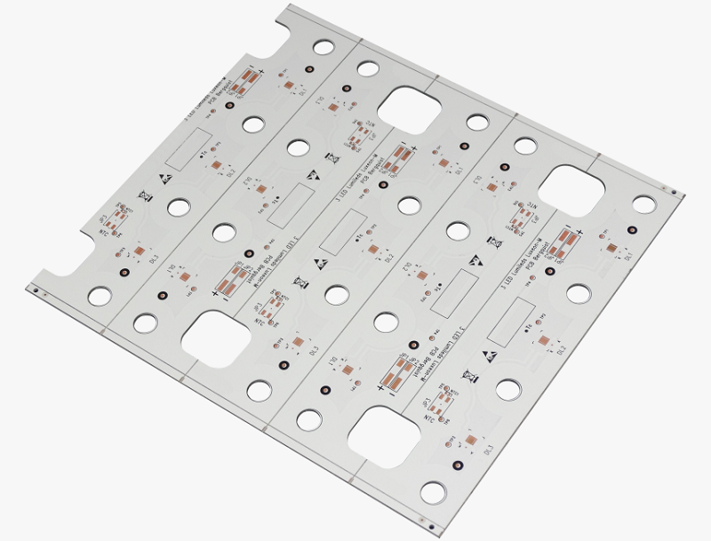
An aluminium based PCB is a powerful choice for modern electronics, especially where heat control matters. Whether you’re designing LED lights, power supplies, or automotive electronics, aluminium PCBs help you manage temperature, protect components, and deliver stable performance. Compared to standard boards, they offer better heat dissipation, which can make a big difference in product reliability.
At EBest Circuit (Best Technology), we manufacture high-quality aluminium PCBs using certified materials and advanced processes. With certifications like ISO9001, ISO13485 for medical devices, IATF16949 for automotive, and UL approval, we provide dependable circuit boards tailored to your needs.
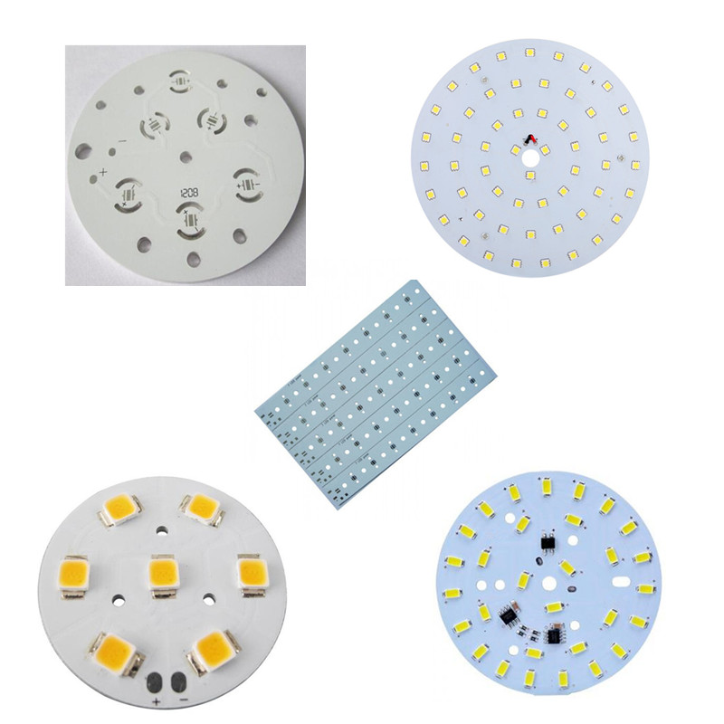
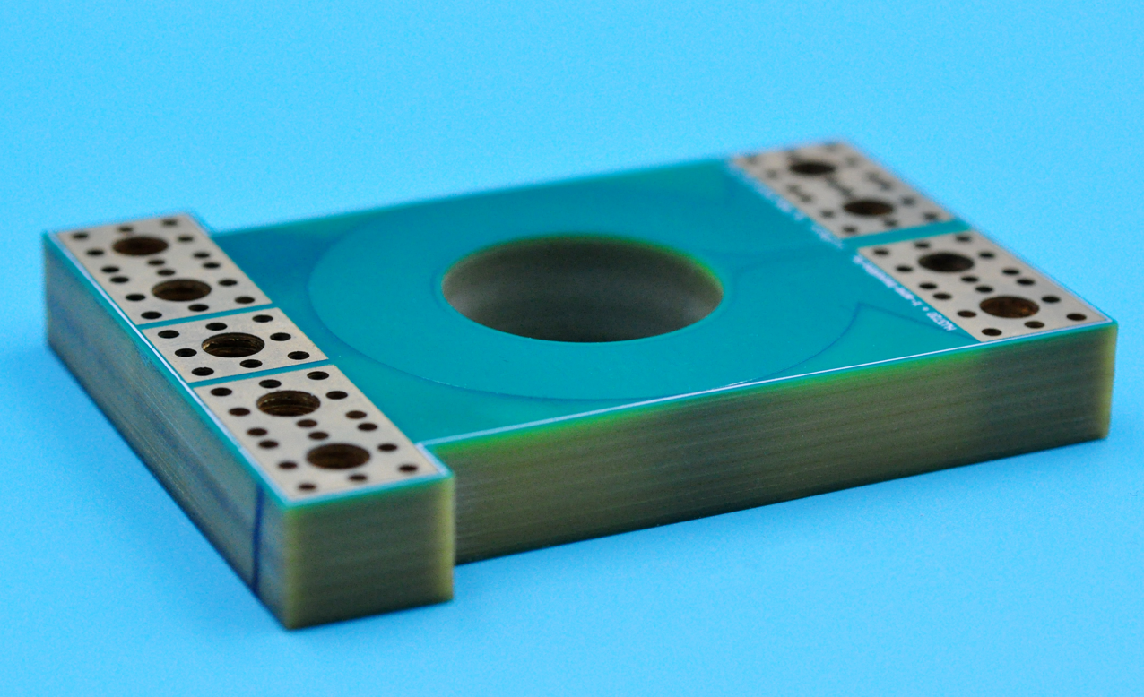
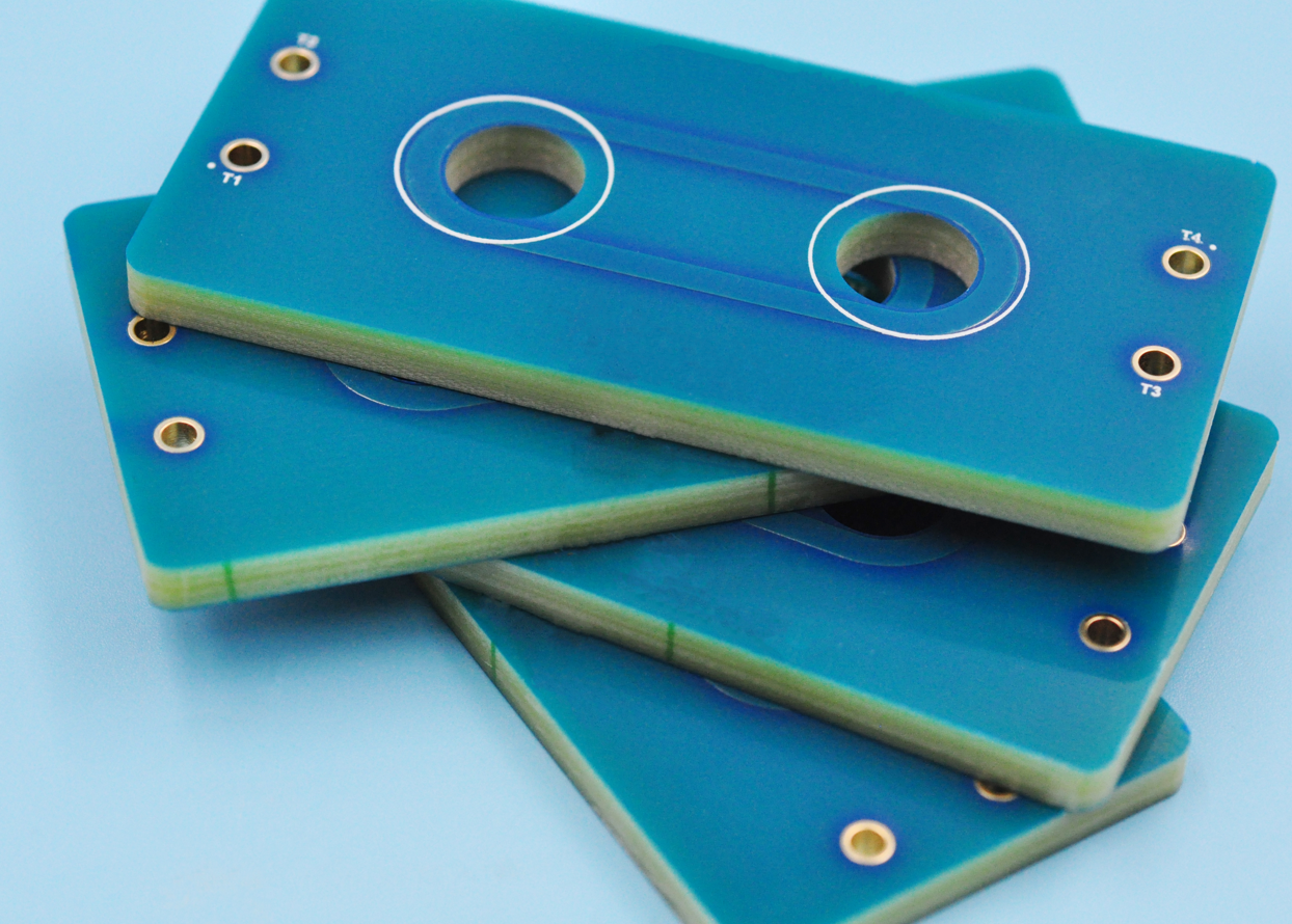
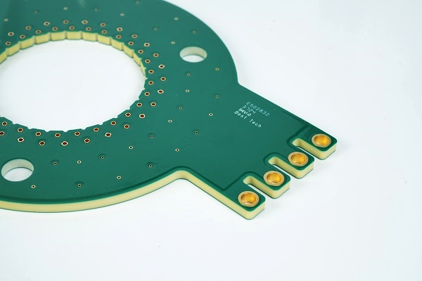
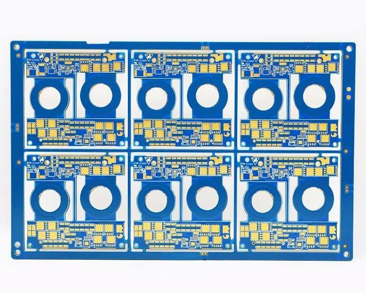
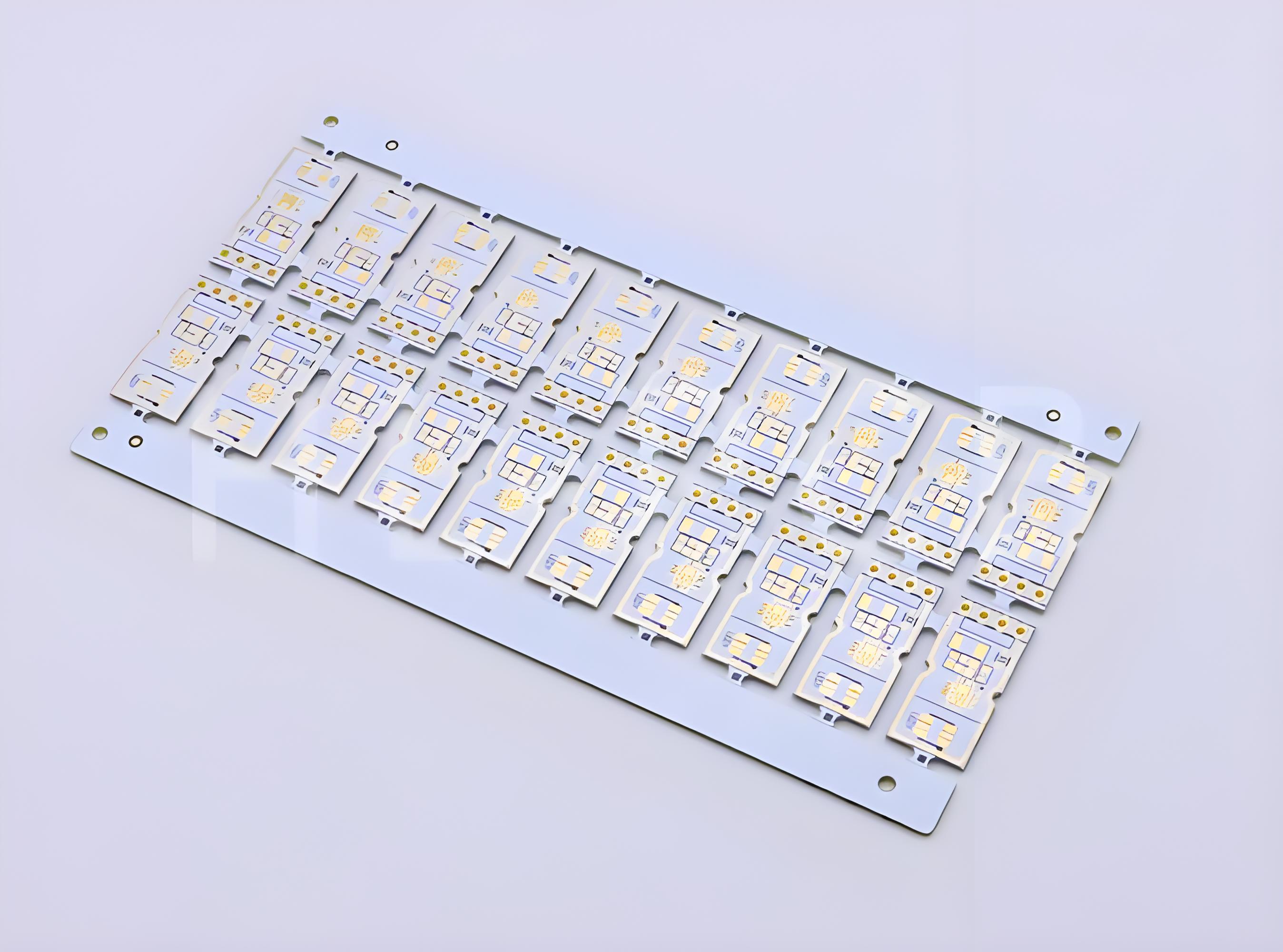
Aluminium Based PCB Manufacturer
What Is Aluminium PCB?
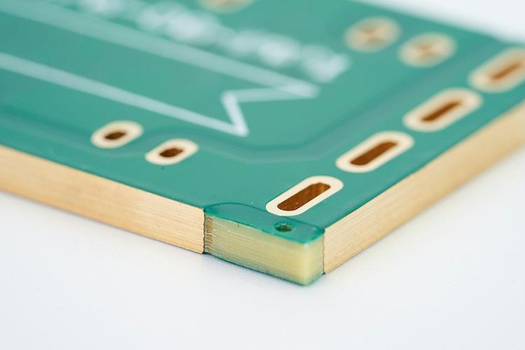
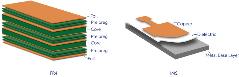
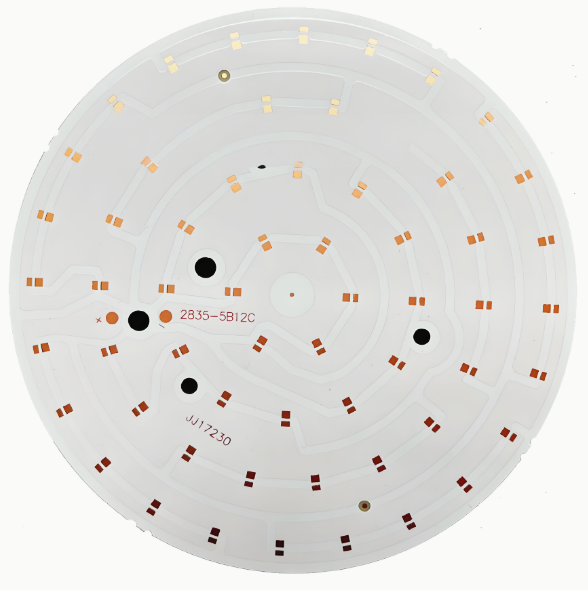
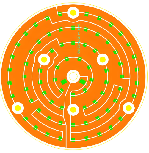
An aluminium PCB—also called a metal core PCB (MCPCB)—is a type of printed circuit board that uses aluminium as the base material instead of the common fiberglass material (FR-4). The board consists of three main layers:
- Aluminium base layer for strength and heat conduction
- Insulating dielectric layer to separate the metal from the copper
- Copper circuit layer for electrical connections
This structure helps draw heat away from heat-sensitive components like LEDs, transistors, or power devices. In simple terms, aluminium PCBs help keep things cool, especially in high-power or high-temperature applications.
What Are the Pros and Cons of Aluminum PCB?
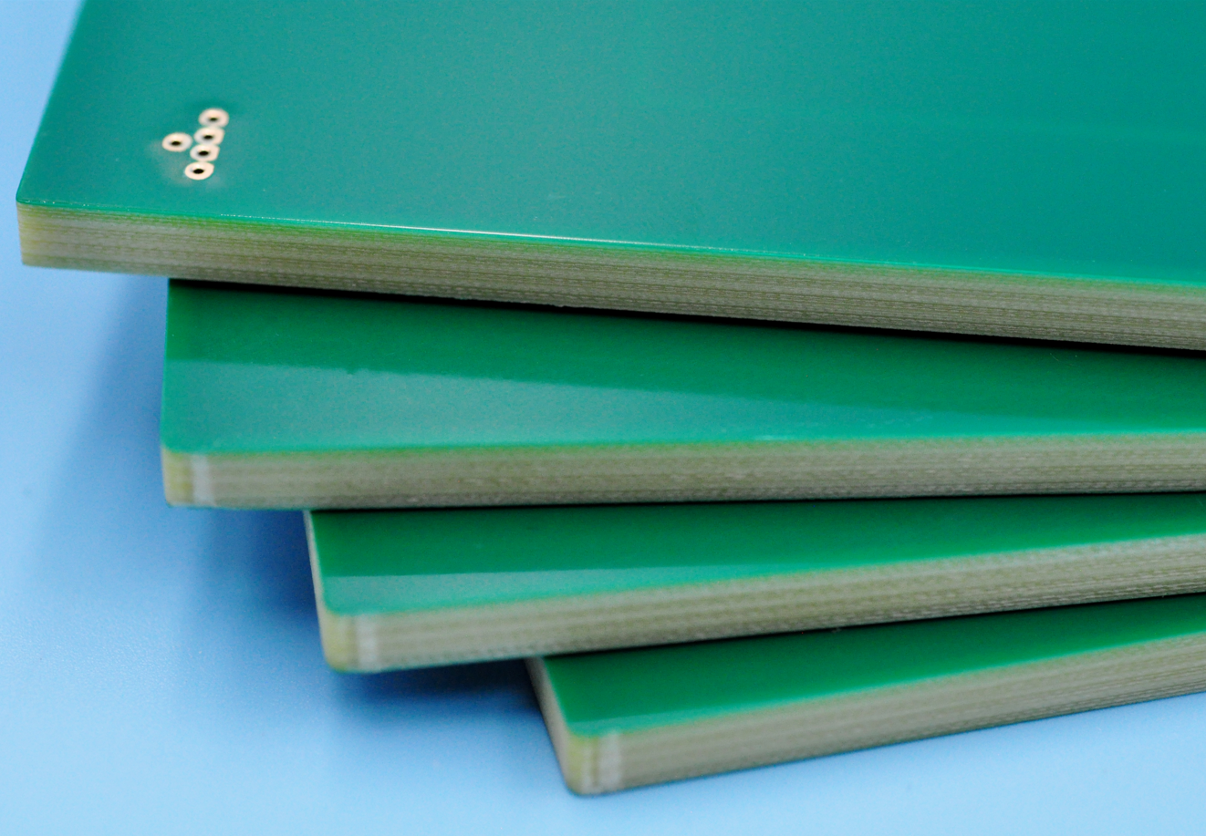
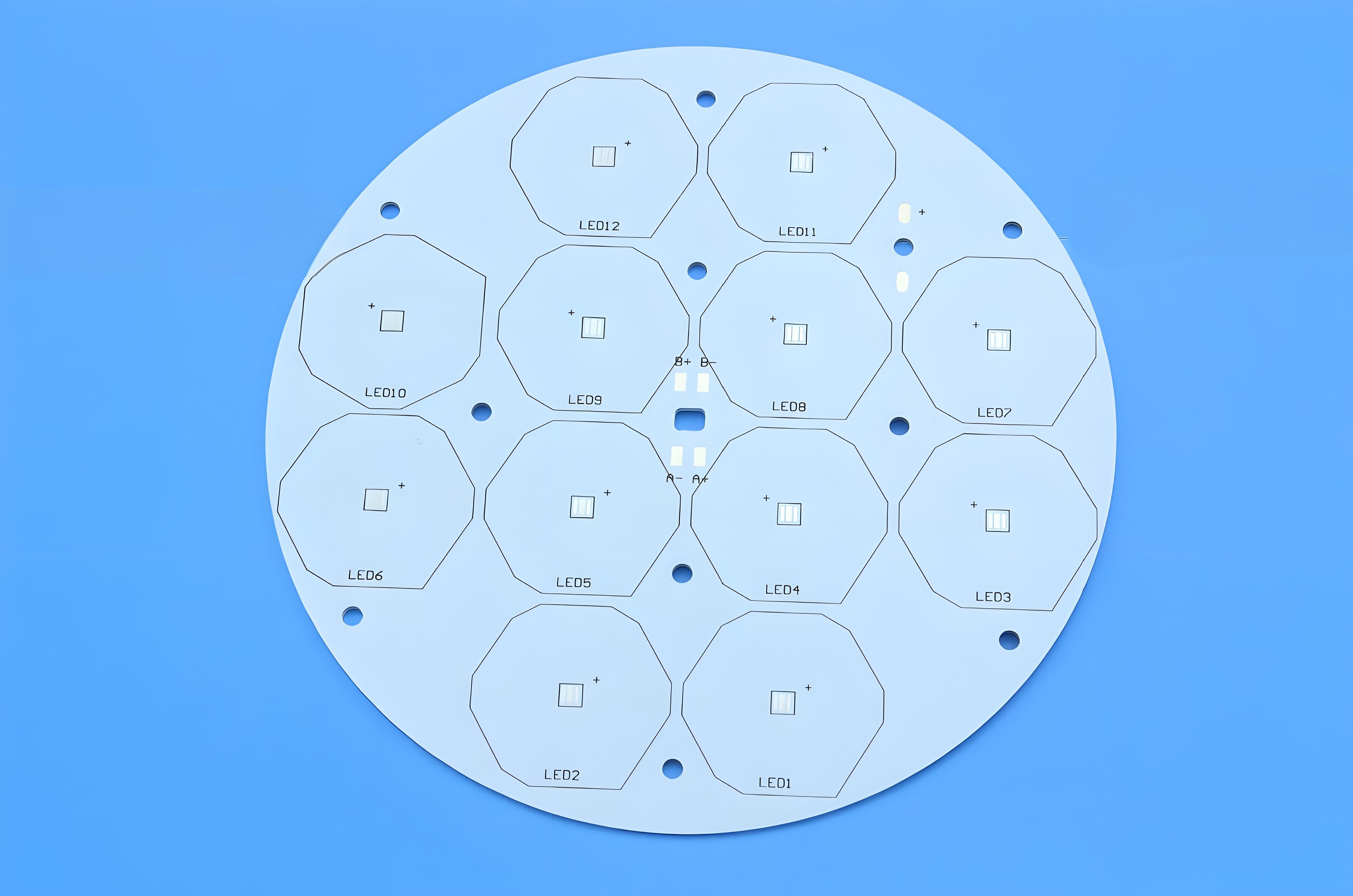
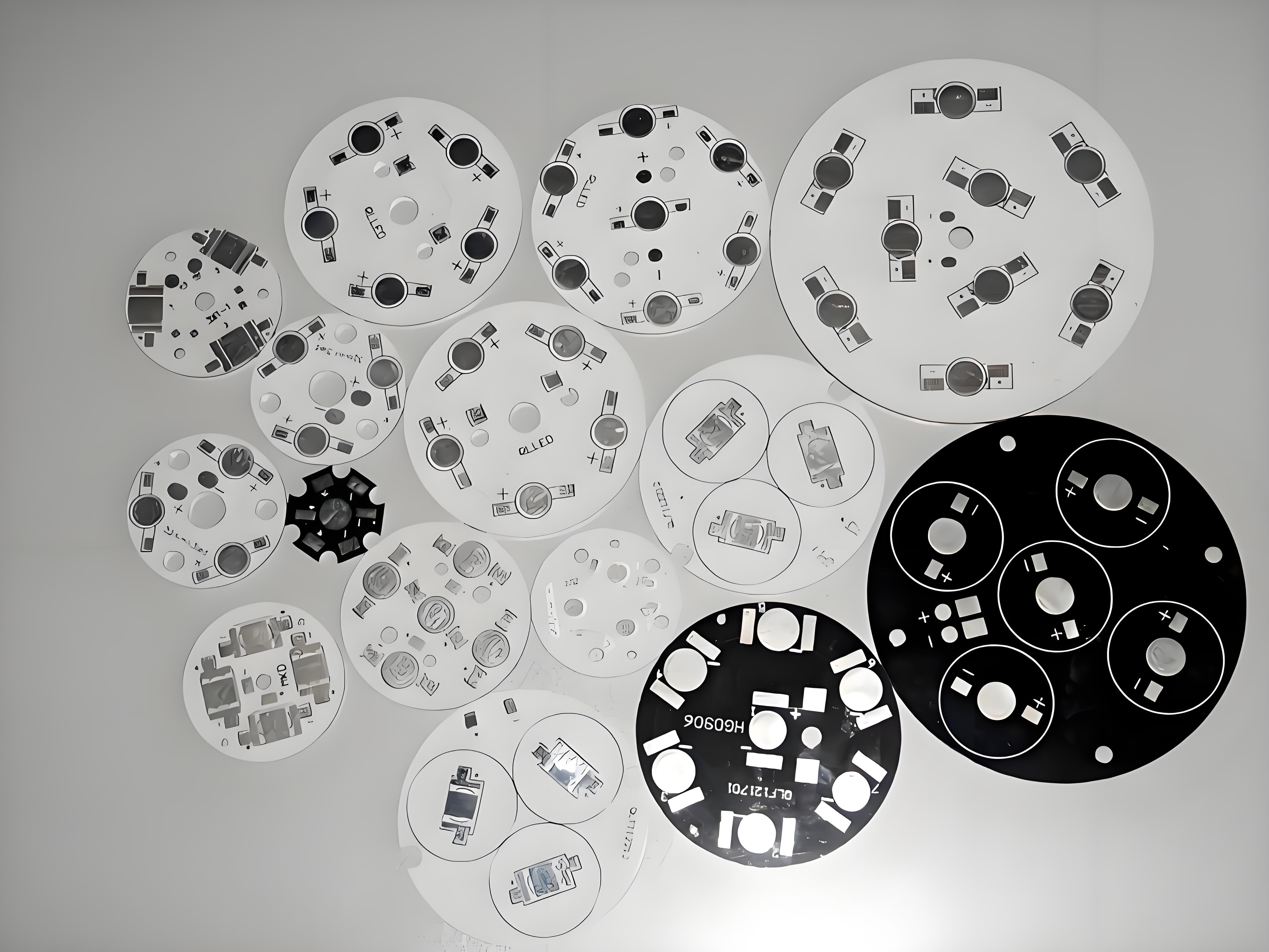
Aluminium-based PCBs are made from low-alloy Al-Mg-Si series high-plasticity aluminium plates (structure shown in the figure below). These boards offer excellent thermal conductivity, electrical insulation, and machinability. Compared to traditional FR-4 boards, aluminium PCBs of the same thickness and trace width can carry higher current. They also feature dielectric breakdown strength up to 4500V and a thermal conductivity greater than 2.0 W/m·K. In the PCB industry, aluminium-based boards are the most widely used metal core PCBs. Key advantages include:
- Support for Surface Mount Technology (SMT)
- Highly efficient thermal diffusion in circuit design
- Lower operating temperature, higher power density, high reliability, and longer product lifespan
- Smaller product size, reducing both hardware and assembly costs
- Replacement for fragile ceramic substrates, offering better mechanical durability
But they also have some limitations:
- Lower flexibility: Aluminium boards cannot be bent like flexible PCBs.
- More complex manufacturing: Special processes are needed to drill and etch metal-based boards.
- Limited layers: Multi-layer aluminium PCBs exist, but they are harder and more expensive to produce.
At EBest Circuit (Best Technology), we help customers balance these factors. Our engineering team guides you through design and material selection to ensure your aluminium PCB works perfectly for your application.
Aluminium PCB Material Properties
Aluminium based PCB typically made from aluminium alloys like 5052, 6061, or 3003. These materials are chosen to handle heat well, maintain electrical insulation, and provide mechanical support. Some customers may confused about them and the differences between these materials. Here EBest Circuit (Best Technology) listing the properties of each material, hope this can help you to choose which one is best for your project.
| Property | 5052 Aluminium | 6061 Aluminium | 3003 Aluminium |
| Composition | Al-Mg alloy | Al-Mg-Si alloy | Al-Mn alloy |
| Thermal Conductivity | ~138 W/m·K | ~167 W/m·K | ~160 W/m·K |
| Electrical Conductivity | ~35% IACS | ~40% IACS | ~40% IACS |
| Tensile Strength | 210–230 MPa | 260–310 MPa | 130–180 MPa |
| Yield Strength | ~130 MPa | ~240 MPa | ~115 MPa |
| Elongation | ~12–20% | ~8–10% | ~10–20% |
| Corrosion Resistance | Excellent | Good | Very Good |
| Formability | Excellent | Good | Excellent |
| Machinability | Fair | Good | Fair |
| Cost | Moderate | Higher | Lower |
| Common Use in PCBs | LED lighting, power electronics | High-power, structural applications | Consumer electronics, general use |
Quick Notes:
- 5052 is favored for excellent corrosion resistance and good thermal performance, often used in outdoor lighting PCBs or marine applications.
- 6061 offers better strength and machinability, suitable for mechanically demanding PCBs or large-size boards.
- 3003 is cost-effective with good thermal and corrosion resistance, ideal for low to moderate power electronic boards.
How Thick Is Aluminum PCB?
Aluminium PCBs vary in thickness based on design and applications needs. Common thicknesses range from 0.8mm to 3.2mm, but custom options are available. Here is a standard aluminium PCB thickness rules:
- Single-layer boards: Typically range from 0.2mm to 0.5mm, suitable for simple circuit designs.
- Double-layer boards: Generally 0.5mm to 1.2mm, balancing both signal transmission and heat dissipation needs.
- Multi-layer boards: Thickness starts from 1.2mm and can reach up to 10mm, ideal for high-power electronic devices.
For applications with high thermal conductivity requirements (such as LED lighting and power electronics), aluminium PCBs may use thinner copper foil (ranging from 35μm to 280μm) laminated with the aluminium base. In such cases, the minimum board thickness can be as low as 0.075mm.
At EBest Circuit (Best Technology), we help customers choose the right thickness based on current flow, heat output, and mechanical strength. Thicker boards may cost more but offer better performance in demanding settings.
What Is the Maximum Temperature for Aluminium PCB?
Aluminium PCBs are built for high-temperature conditions. The dielectric layer determines the maximum working temperature, which typically ranges between 130°C to 150°C. Special materials can go higher, depending on the design.
Why is this important? In LED lighting or automotive power modules, excess heat can damage components. By using aluminium PCBs, you keep the temperature down and extend the life of your product. If you want to used in extreme high temperature applications, we have ceramic PCB that can achieve 850°C.
Aluminium PCB Manufacturing Process – Simplified
1. Material preparation: Select the right aluminium base, apply dielectric material, and add copper foil.
2. Drilling: CNC machines create holes for vias and component placement.
3. Circuit imaging: A photoresist is applied, and UV light is used to define the circuit pattern.
4. Etching: Unwanted copper is removed, leaving only the desired circuit.
5. Plating: Through-hole plating may be used if needed for connections.
6. Solder mask application: A protective layer prevents oxidation and solder bridging.
7. Surface finish: Common finishes include ENIG (Electroless Nickel Immersion Gold), HASL (Hot Air Solder Leveling), or OSP (Organic Solderability Preservative).
8. Testing: Electrical and thermal tests ensure each board performs as required.
Below is the detailed aluminium based PCB manufacturing process. EBest Circuit (Best Technology) uses advanced MES systems for full traceability and tight quality control. We support both prototype runs and mass production with fast turnaround times.
How Does an Aluminium Based PCB Cost?
Several factors influence the cost of aluminium PCBs:
- Material grade: Higher-quality aluminium and thermal materials cost more.
- Board size and complexity: Larger boards or intricate designs increase price.
- Copper thickness: Thicker copper adds to material and processing costs.
- Surface finish: ENIG is more expensive than HASL or OSP.
- Quantity: Bulk orders lower per-unit costs.
In general, aluminium PCBs cost more than FR-4 for simple designs but offer cost savings in thermal management. For example, using aluminium boards can eliminate the need for extra heat sinks or cooling fans. At EBest Circuit (Best Technology), we offer competitive pricing and help you optimize design for cost and performance.
What Is the Difference Between Aluminum PCB and FR-4?
The main difference between aluminum PCBs and FR-4 PCBs lies in the base material and how each board handles heat and mechanical stress.
Aluminum PCBs use a metal base (usually aluminum) that helps conduct heat away from components. This makes them a great choice for high-power circuits like LEDs and power supplies. In contrast, FR-4 PCBs are made from fiberglass material. They are versatile and cost-effective but have poor thermal conductivity, which can be a problem in heat-sensitive designs. Here’s a quick side-by-side comparison:
| Feature | Aluminum PCB | FR-4 PCB |
| Base Material | Aluminum (metal core) | Fiberglass (FR-4) |
| Thermal Conductivity | High (1.0–3.0 W/m·K) | Low (~0.3 W/m·K) |
| Heat Dissipation | Excellent | Limited |
| Strength | Strong and durable | Moderate |
| Flexibility | Low (rigid) | Higher (can be rigid or flexible) |
| Cost | Slightly higher (for materials) | Lower for basic designs |
| Typical Use | LEDs, power electronics, automotive | Consumer electronics, general use |
Use aluminium PCBs when your design needs to handle heat efficiently and survive tough environments. Use FR-4 when thermal demands are low, or you need flexible or multi-layer boards.
When to Use Aluminum PCB?
Aluminium PCBs are the right choice when you need:
- Efficient heat dissipation
- Reliable performance in high-power applications
- Space-saving designs without extra heat sinks
Common applications include:
- LED lighting systems (e.g., streetlights, automotive lamps)
- Power converters and inverters
- Battery chargers
- Audio amplifiers
- Telecom and base stations
If your design struggles with overheating or if your product needs to run 24/7 without failure, aluminium PCBs can help you achieve that.
At EBest Circuit (Best Technology), we specialize in custom aluminium PCBs with strict quality standards and professional support. Whether you need single-layer, multi-layer, or special-shaped boards, we’ve got you covered. Ready to explore aluminium PCB solutions? Contact EBest Circuit (Best Technology) today for a quote or technical consultation.
FAQs
1. Can aluminium PCBs be used in flexible applications?
No, aluminium PCBs are rigid. If you need flexibility, consider flexible PCBs or hybrid designs.
2. Are aluminium PCBs more expensive than FR-4?
Yes, but they reduce the need for additional cooling, saving costs in the long run.
3. Can I use aluminium PCBs for RF applications?
Yes, with the right dielectric material, aluminium PCBs can work in RF circuits.
4. How fast can I get aluminium PCBs from EBest Circuit (Best Technology)?
We offer fast lead times, depending on design and quantity. Contact us for details.
5. Do you provide samples for testing?
Yes, we support prototype orders to help you test and finalize your design.