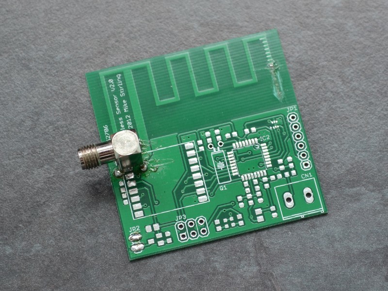
5G antenna PCB is a printed circuit board engineered to support high-frequency antenna structures, stable RF transmission, and compact wireless integration in modern 5G devices. This article explains what a 5G antenna PCB is, how it is designed, which materials and structures are used, and how to choose a reliable manufacturer for design, prototyping, and assembly.
Common customer pain points:
Corresponding solutions:
- Co-design antenna layout, stack-up, and matching networks early.
- Select low-loss materials based on frequency and efficiency targets.
- Conduct DFM reviews focused on RF-critical structures.
- Provide rapid prototyping with stable process control.
- Offer one-stop PCB fabrication and assembly services.
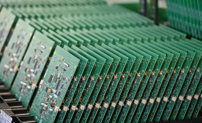
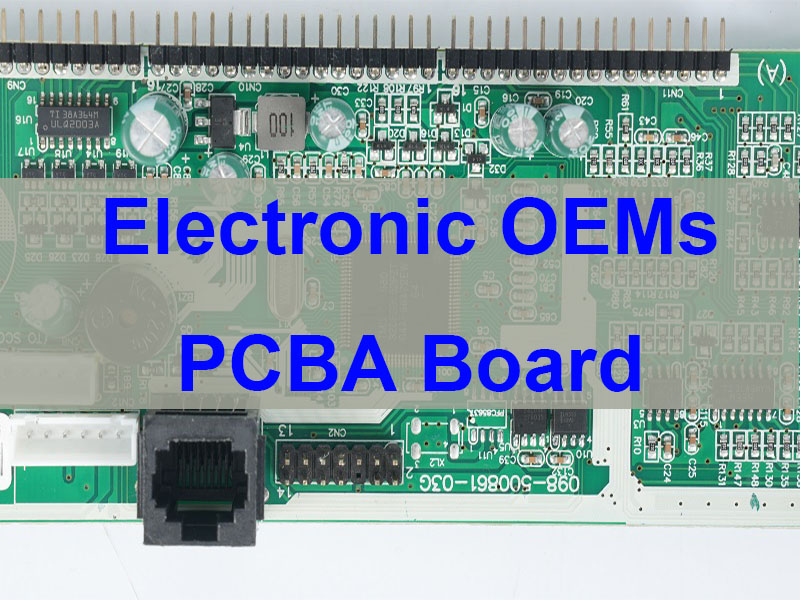
EBest Circuit (Best Technology) is an engineering-driven PCB and PCBA manufacturer specializing in RF and antenna PCB solutions. With integrated capabilities from design review to assembly, we help customers reduce iteration risk and accelerate product development. For inquiries, please contact sales@bestpcbs.com.
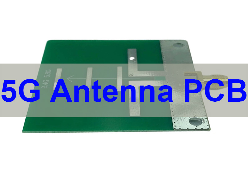
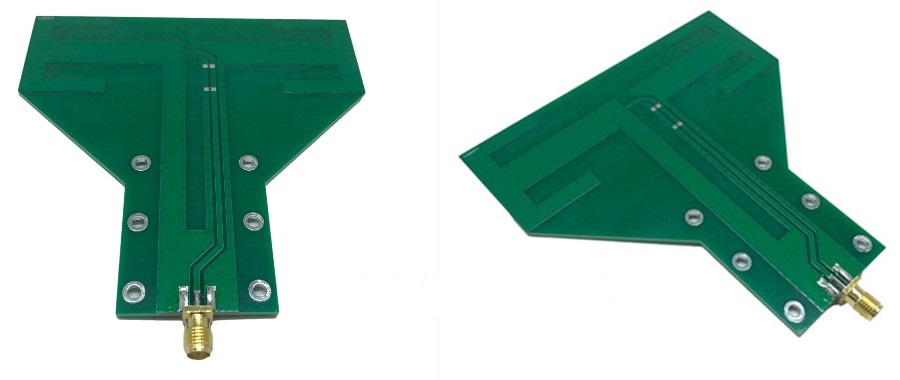
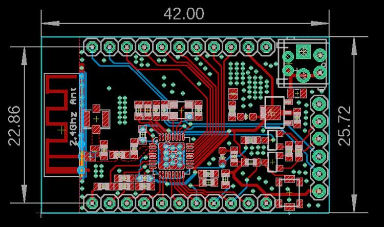
What Is a 5G Antenna PCB?
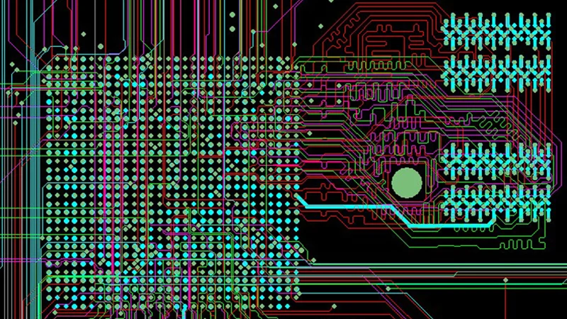
A 5G antenna PCB is not simply a circuit board with an antenna pattern. In reality, it is a highly integrated RF platform where antenna geometry, dielectric material, copper structure, and layout all directly influence signal behavior.
Key characteristics:
- Integrates antenna directly into PCB structure
- Supports sub-6 GHz and mmWave frequency bands
- Requires precise impedance and loss control
- Often used in MIMO or multi-antenna systems
- Sensitive to layout, grounding, and surrounding components
5G communication typically operates across two major frequency domains: sub-6 GHz and mmWave, and each range places very different demands on antenna size, material selection, and layout precision. In practical engineering, sub-6 GHz designs prioritize coverage and stability, while mmWave solutions focus more on bandwidth, beam control, and array integration.
In essence, a 5g pcb antenna is both a structural and electrical component that defines wireless performance.
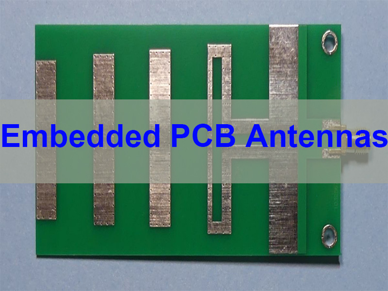
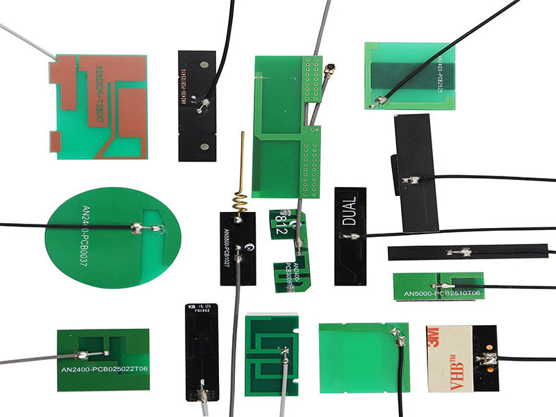
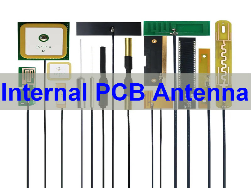
What Are the Types of 5G Antenna PCBs?
Different applications require different antenna structures, and selecting the right type is critical for performance.
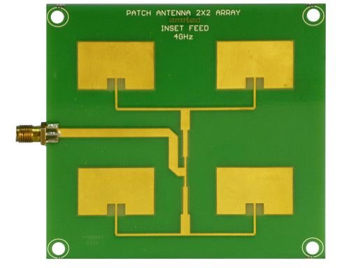
Common types:
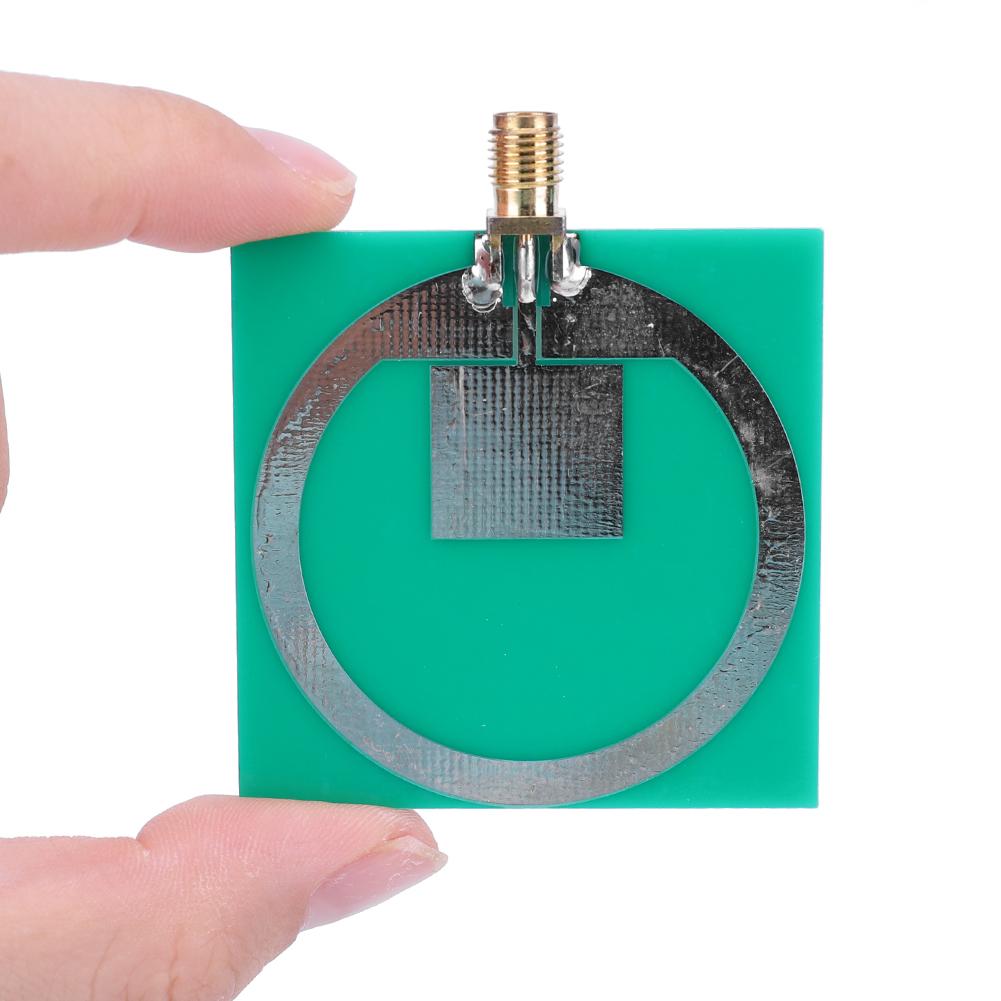
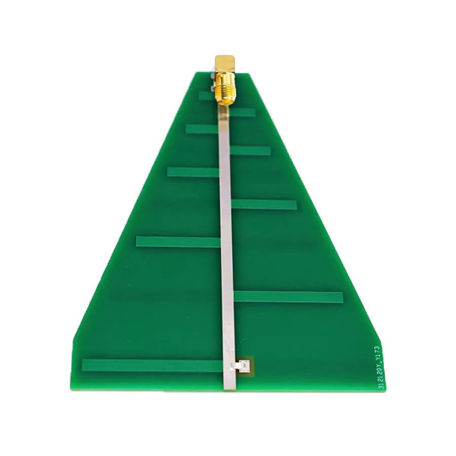
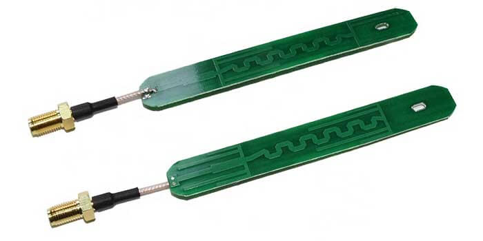
- Patch antenna PCB
- PIFA / IFA antenna PCB
- Slot antenna PCB
- Dipole / monopole PCB antenna
- Array antenna PCB
- Flexible PCB antenna
Comparison:
| Type | Advantage | Application |
|---|---|---|
| Patch | Directional gain | Base stations |
| PIFA | Compact | Mobile devices |
| Slot | Flexible layout | Shielded systems |
| Dipole | Simple design | External antennas |
| Array | Beamforming | mmWave systems |
| Flexible | Space-saving | Wearables |
Each type must align with enclosure design, ground reference, and frequency band.
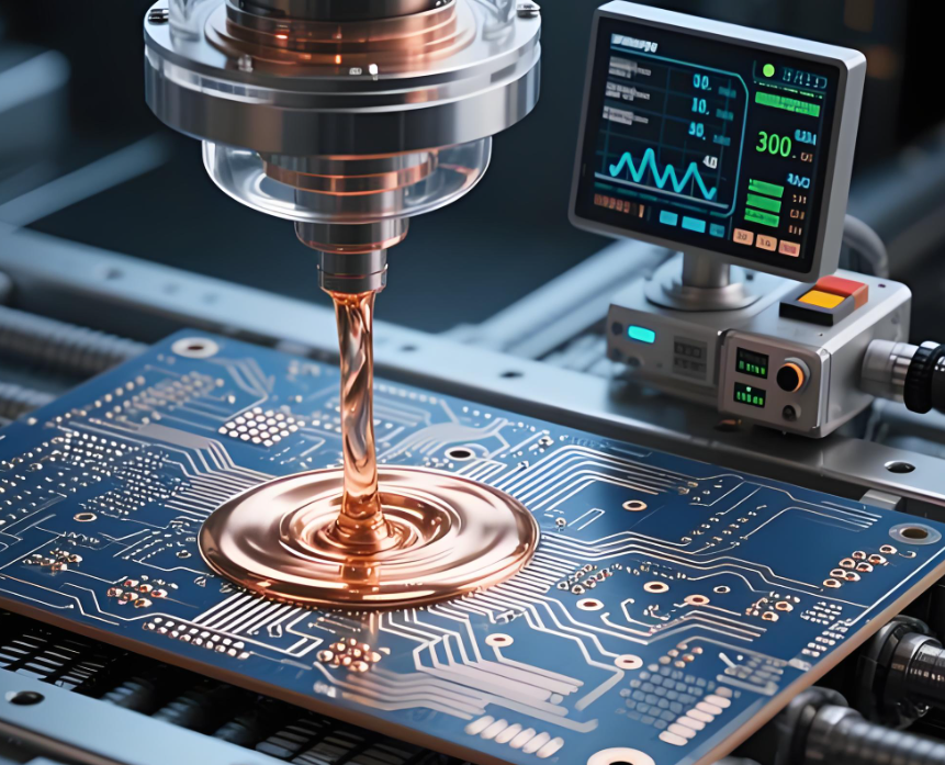
What Materials Are Used in 5G Antenna PCBs?
Material selection is one of the most critical factors in 5g antenna pcb manufacturing.
Common materials:
- FR-4
- Rogers
- PTFE-based laminates
- LCP
- Hybrid stack-ups
Material comparison:
| Material | Cost | RF Performance | Usage |
|---|---|---|---|
| FR-4 | Low | Limited | Entry-level |
| Rogers | Medium | High | RF boards |
| PTFE | High | Excellent | Microwave |
| LCP | Medium | Strong | Compact antennas |
| Hybrid | Medium | Balanced | Cost-performance |
In high-frequency PCB design, material selection is not just about dielectric constant, but also about loss tangent stability, copper surface profile, and thickness consistency. As operating frequency increases, even small variations in these parameters can significantly impact signal integrity and antenna efficiency.
Therefore, choosing the right material is a balance between performance requirements and cost constraints.
What Are the Applications of 5G PCB Antennas?
The adoption of 5g pcb antenna supplier solutions is rapidly expanding across industries.
Key applications:
- 5G routers and CPE
- Industrial IoT devices
- Automotive communication systems
- Telecom infrastructure
- Smart healthcare devices
- Wireless modules
Why they matter:
- Higher data rates require efficient antennas
- Compact devices need integrated designs
- Multi-antenna systems require isolation control
These applications demand not only manufacturing capability but also strong RF understanding.
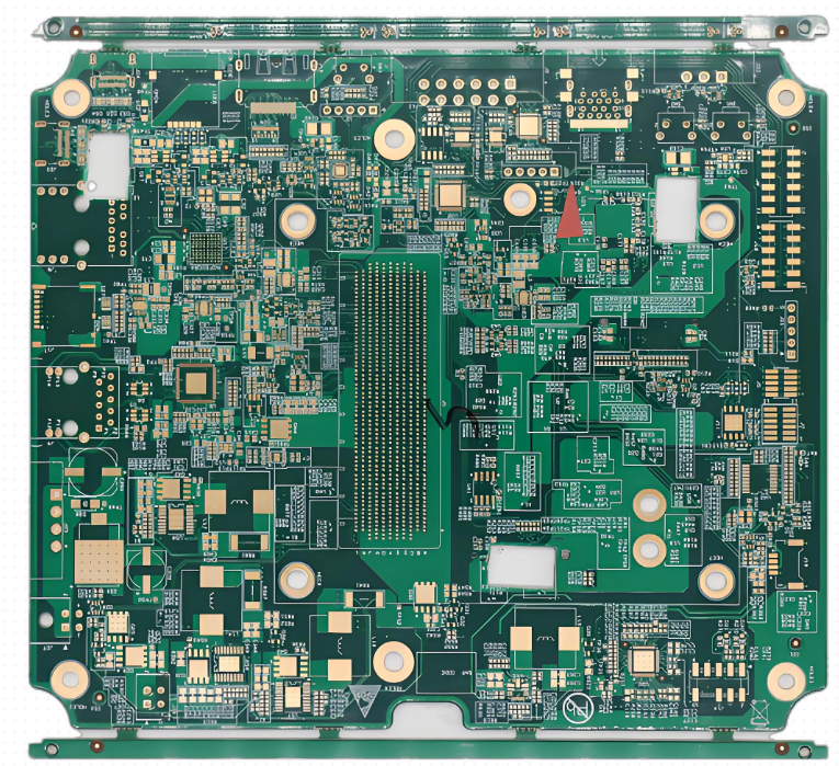
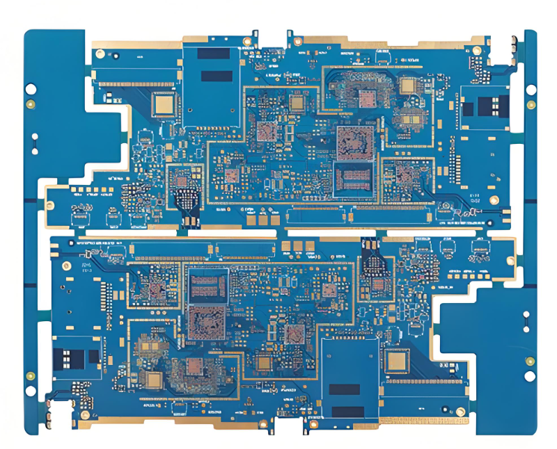
Top 10 5G PCB Antenna Factories in China
This list focuses on companies with strong RF, telecom, or antenna PCB capabilities.
- EBest Circuit (Best Technology)
- Shennan Circuits
- Kinwong
- Suntak
- Founder PCB
- Victory Giant Technology
- WUS Printed Circuit
- C&T RF Antennas
- Asian Creation Communication
- Victory PCB
Different manufacturers specialize in different areas, such as high-volume production, RF expertise, or rapid prototyping.
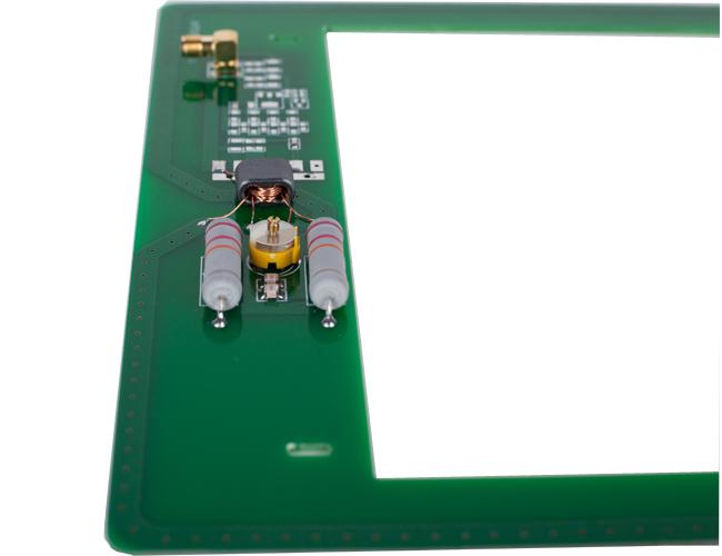
How to Design a Reliable 5G Antenna PCB?
A reliable 5g antenna pcb manufacturing process starts with proper design decisions.
Key design practices:
- Define operating frequency early
- Choose appropriate materials
- Maintain antenna clearance zones
- Optimize feed and matching network
- Control grounding and shielding
- Validate with simulation and testing
Designing a reliable 5G antenna PCB requires more than following standard PCB rules. Engineers must consider antenna placement, ground continuity, and interaction with nearby components early in the design stage.
For advanced 5G systems, antenna arrays and beamforming structures are often used, which require tighter layout symmetry and manufacturing precision.
Although simulation tools are essential, real-world testing remains critical because enclosure effects and manufacturing variations can impact performance.
What Are the Pros and Cons of 5G Antenna PCBs?
Advantages:
- Compact integration
- Reduced assembly complexity
- Better repeatability
- Suitable for MIMO systems
Limitations:
- Sensitive to layout changes
- Higher material requirements
- Requires multiple iterations
- More complex manufacturing
Summary table:
| Aspect | Advantage | Limitation |
|---|---|---|
| Integration | Compact | Hard to modify |
| Cost | Reduced BOM | Material cost |
| Performance | High efficiency | Sensitive |
| Scalability | Production-ready | Requires control |
Working with an experienced 5g pcb antenna factory helps minimize these challenges.
How to Select a Reliable 5G PCB Antenna Manufacturer?
Choosing the right 5g pcb antenna supplier is essential.
Key criteria:
- RF design understanding
- Material expertise
- Prototyping capability
- DFM support
- One-stop service
- Industry experience
- Communication efficiency
Evaluation table:
| Criteria | Requirement |
|---|---|
| RF knowledge | Understand antenna behavior |
| Materials | Recommend based on frequency |
| Prototyping | Fast and reliable |
| Process | Stable and traceable |
| Service | PCB + Assembly |
A good manufacturer should act as a technical partner, not just a supplier.
In conclusion, 5G antenna PCB is a critical platform that enables efficient wireless communication by integrating antenna performance with PCB design and manufacturing. This article covered its types, materials, applications, design strategies, and supplier selection considerations. EBest Circuit (Best Technology) provides complete solutions from RF design support to PCB fabrication and PCBA assembly, helping customers accelerate development and reduce risks. If you are looking for a reliable 5g pcb antenna manufacturer, feel free to contact us at sales@bestpcbs.com.
FAQs About 5G Antenna PCBs
1. Can FR-4 be used for 5G antenna PCB?
Yes, for some sub-6 GHz designs, but not ideal for higher frequencies.
2. Is 5G antenna PCB always high-frequency PCB?
Yes, due to RF requirements.
3. Why is prototyping important?
Because real performance differs from simulation.
4. What affects antenna performance most?
Material, layout, grounding, and environment.
5. What is one-stop service?
Design, PCB fabrication, and assembly in one workflow.