PCB manufacturing PCB manufacturing
Home > Blog

Why are some PCBs black? Does the color of PCB matter?

January 2nd, 2025

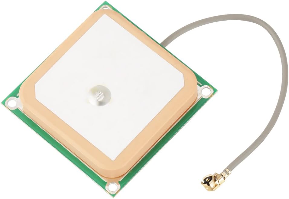
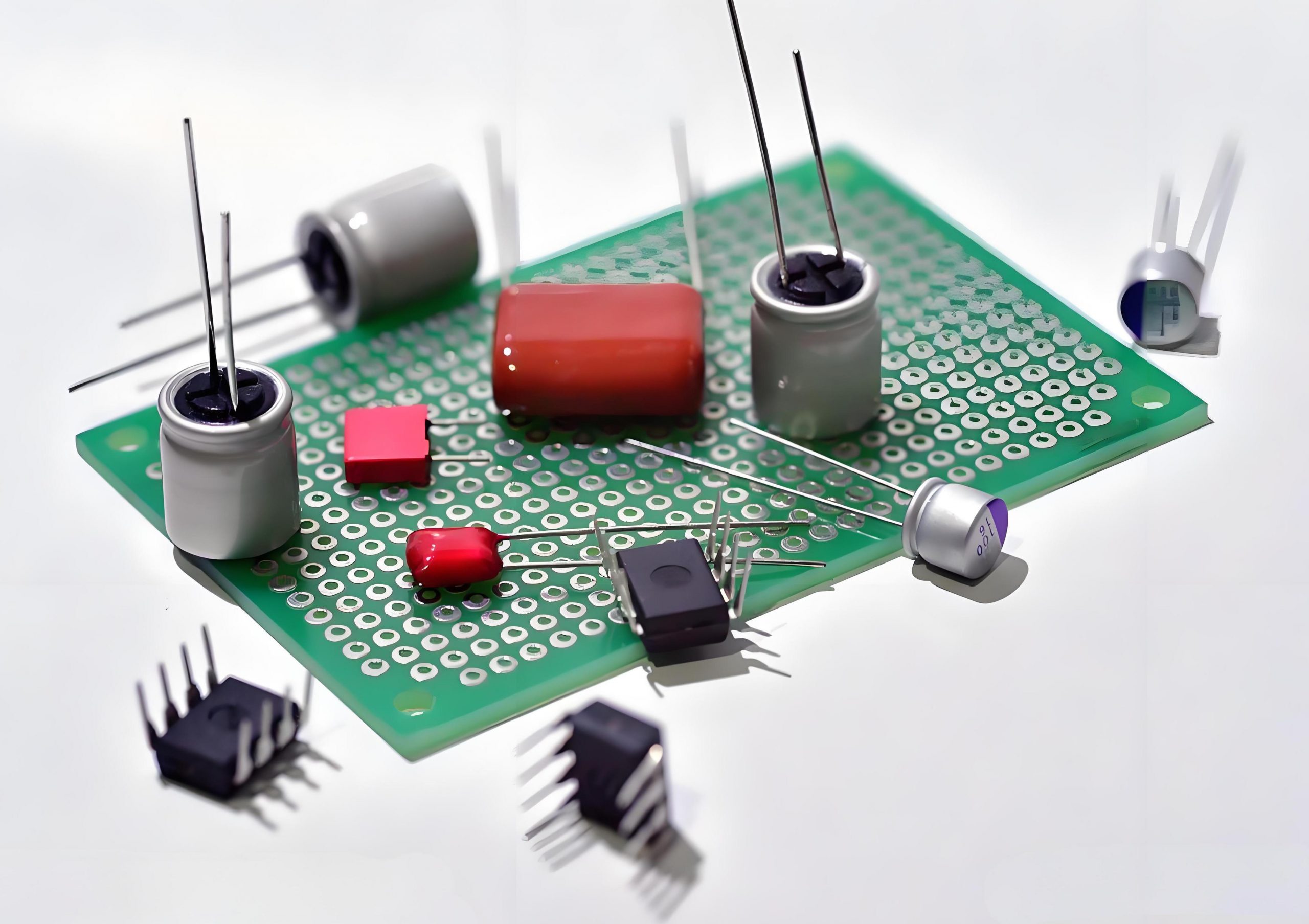
Why are some PCBs black? Mainly because of the color choice of solder resist. Black pigment is added to solder resist, and black solder resist has good light shielding and resolution. From the performance point of view, black PCB may help to resist electromagnetic interference, and its coating or material components can absorb or shield electromagnetic radiation. In addition, the black surface has advantages in thermal radiation, and it is easier to absorb and emit radiant heat, which is conducive to heat dissipation.

Why are PCBs black?

The black PCB is mainly because its surface is usually coated with a layer of black solder resist. This layer of solder resist not only provides protection for the circuit board, preventing the circuit from being damaged by moisture, dust and other factors in the environment, but also effectively shields the circuit traces below, increasing the beauty and overall sense of the product.

Why are some PCBs black? Does the color of PCB matter?

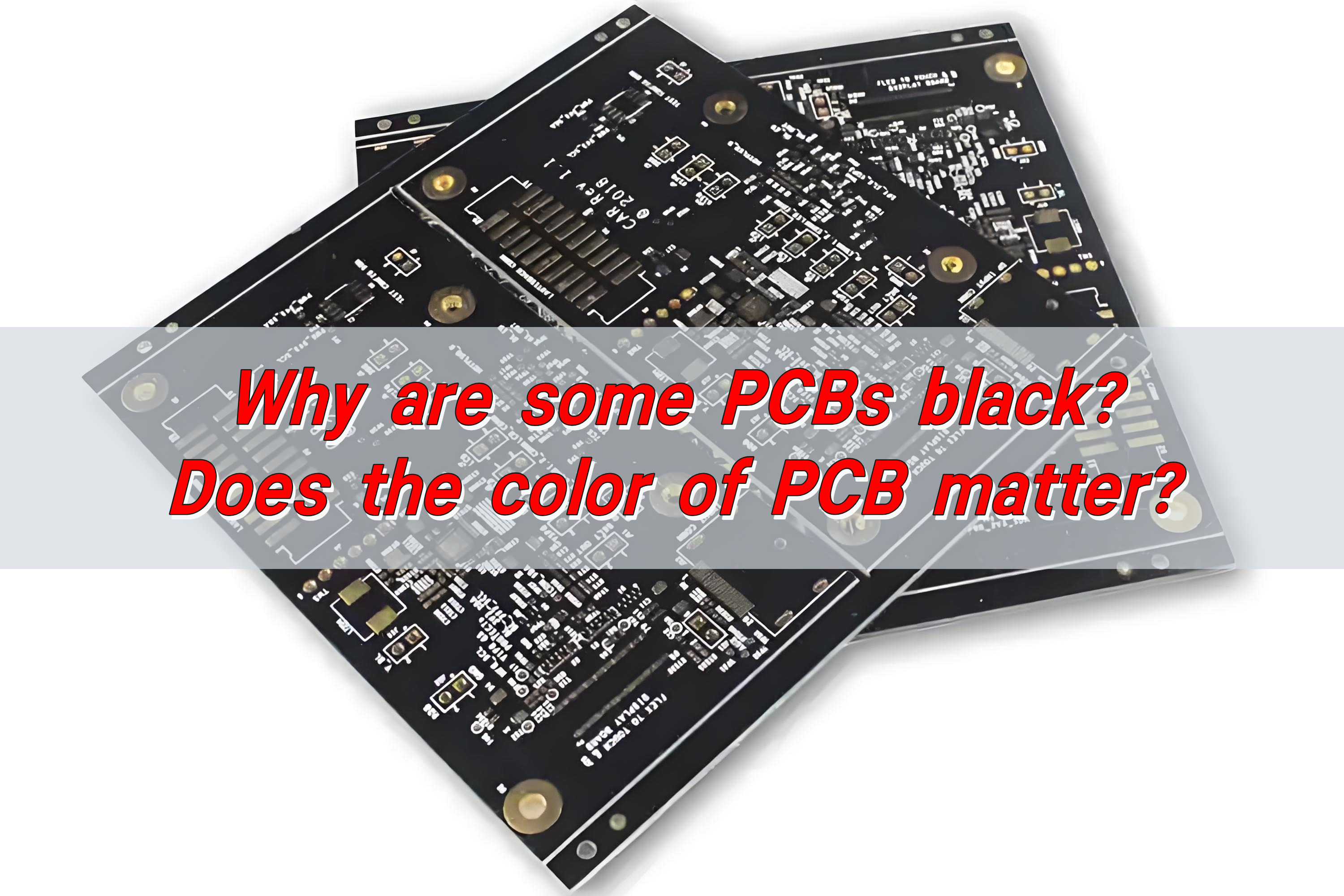
In addition, black PCB also has its specific application background and market demand in the electronics industry. In the early days, black PCB mainly appeared in high-end electronic products, such as computer motherboards and graphics cards, giving people a high-end and professional feeling. They used black PCB as one of the symbols of high-end motherboards, and then other manufacturers followed suit.

However, there is no essential difference in the manufacturing process and method of PCBs of different colors. Black PCBs are simply made of special colored epoxy resin, which will increase the manufacturing cost to a certain extent, and the circuit traces of black PCBs are difficult to identify, which will increase the difficulty of maintenance and debugging in the R&D and after-sales stages.

Nevertheless, black PCBs do not reduce their electrical performance, and PCBs of different colors are the same in electrical performance.

Why are black PCBs more expensive?

The main reasons for the higher cost of black PCBs include material costs and the complexity of the manufacturing process.

First, black PCBs use special colored epoxy resin, which is relatively rare, so the cost is higher. In addition, black PCBs require higher precision and more complex processes during the manufacturing process, which also increases their cost.

Specifically, the manufacturing process of black PCBs is basically the same as that of green or other colored PCBs, but black PCBs require the use of special colored epoxy resin, which is relatively rare, resulting in increased costs.

In addition, black PCBs may not be as superior to green PCBs in optical positioning calibration and visual effects, which may also affect their market acceptance and price.

Is black PCB better than green?

Black PCB and green PCB have their own advantages and disadvantages. Choosing which one is better depends on the specific application requirements.

Advantages and Disadvantages of Black PCB

Advantages:

  • Signal isolation and electromagnetic interference control: Black PCB can provide better signal isolation and electromagnetic interference (EMI) control, suitable for high-frequency circuits and high-speed signal transmission circuits.
Why are some PCBs black? Does the color of PCB matter?
  • Appearance and high-end feeling: Black PCB is usually used in high-end applications, which can enhance the overall appearance and high-end feeling of the product1.

Disadvantages:

  • Complex production process: The production process of black PCB is relatively complex. Due to the strong absorption of light by black pigment, it is easy to have process problems in the exposure and development processes, resulting in a high scrap rate and relatively high cost.
  • Difficulty in maintenance: The surface wiring of black PCB is almost completely covered, which is difficult to repair, and the difficulty of hole is high, the yield rate is low, and the price is relatively high.

Advantages and Disadvantages of Green PCB

Advantages:

  • Low cost: Green PCB is the most common color, with mature production process and low cost.
  • High visibility: Green PCBs have a high contrast with white text, are highly readable, and reflect less light, which helps reduce glare.
  • Environmentally friendly: Green solder mask ink is more environmentally friendly when it is discarded and is more convenient to recycle.

Disadvantages:

  • Average signal isolation effect: Green PCBs are not as good as black PCBs in signal isolation and EMI control.
  • Ordinary appearance: Green PCBs are usually used for general purposes and are not as high-end as black PCBs.

Does the color of PCB matter?

The color of the PCB has a certain impact on the design, manufacturing, and performance of the circuit board, but it does not determine its quality.

The impact of PCB color on the circuit board

  • Physical and chemical properties: PCBs of different colors may use different production processes and materials, which affects their physical and chemical properties.
  • Cost: Color selection also affects cost. Green PCBs are the most common choice because their production process is mature and cost-effective. PCBs of other colors may require more expensive materials or production processes.
  • Aesthetics and design requirements: Some high-end electronic products may choose non-green PCB colors, such as blue or black, for a unique appearance. In addition, different colors also have different application requirements in the design and manufacturing process.

Why are most motherboards black?

The main reasons why most motherboards are black include visual habits, aesthetics, and functionality.

First, the design of black motherboards conforms to the visual habits of programmers and hardware engineers, making the program code and circuit board more coordinated.

Why are some PCBs black? Does the color of PCB matter?

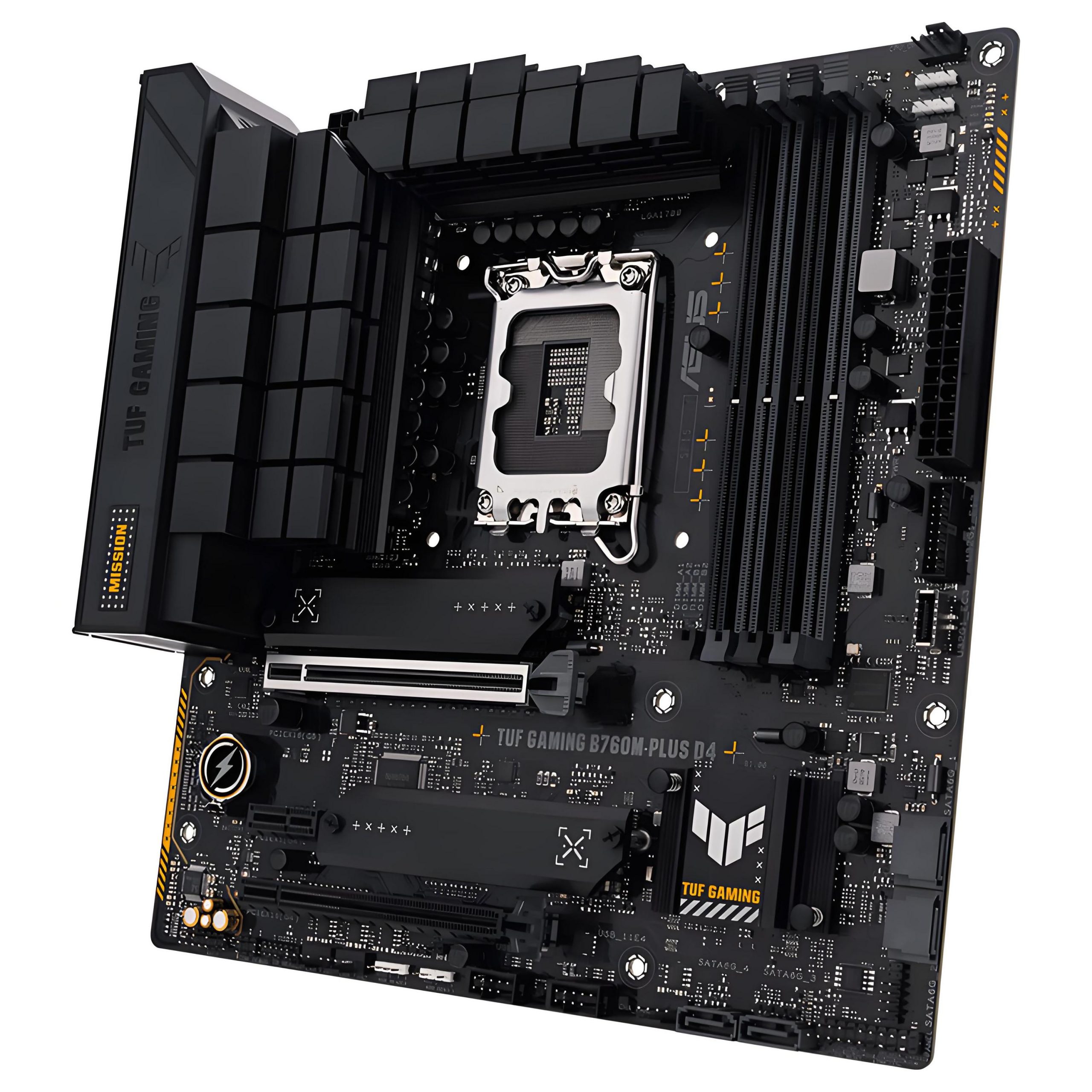
In addition, black motherboards can hide stains and dust on the circuit board, maintain the beauty of the host, and will not conflict with other hardware colors, making the appearance of the entire computer more harmonious. Black materials also have anti-corrosion and heat dissipation properties, which can extend the service life of the motherboard.

Second, from the perspective of production and manufacturing, black motherboards do not add additional costs. Different colors of solder resist only have different visual effects, but do not affect the performance and cost of the motherboard. The popularity of black motherboards is not due to low cost, but because of its visual effects and functional advantages.

Finally, black has a mysterious and low-key cultural quality, which also makes black motherboards more popular in the high-end market. In addition, the superior heat dissipation performance of black motherboards contributes to the long-term and stable operation of electronic products.

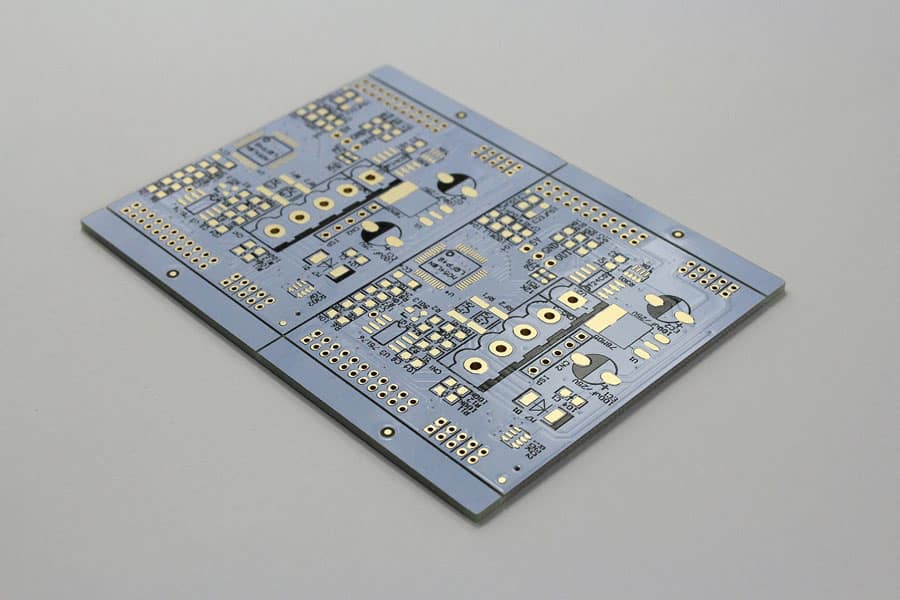
Why are some PCBs blue?

The main reasons for the use of blue PCBs include its good appearance and recognition, high contrast of screen printing, and advantages in specific applications.

First, blue PCBs are often seen as thick boards for labels because they provide significant screen printing contrast. This color is not as visually striking as green, black, or white, but it provides an excellent aesthetic choice. Blue PCBs are particularly advantageous when mounting LCD devices because they do not produce sharp contrasting edges and bright background colors.

Why are some PCBs black? Does the color of PCB matter?

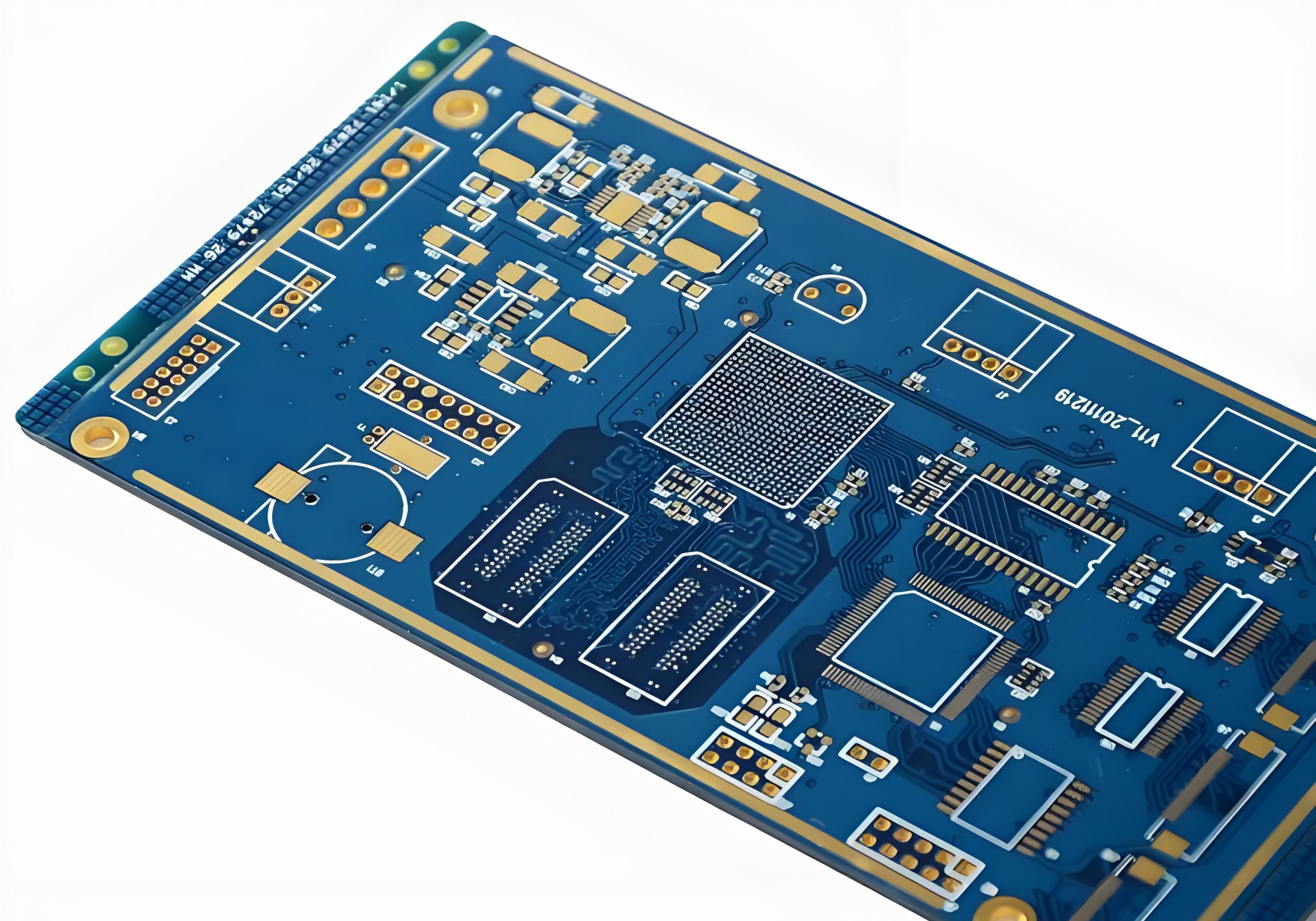
In addition, blue PCBs also have their unique advantages in specific applications because they use high-temperature resistant blue photosensitive dyes, and these dyes have good thermal stability and weather resistance, so they are suitable for use in high temperature and harsh environments.

What is the most common color of PCB?

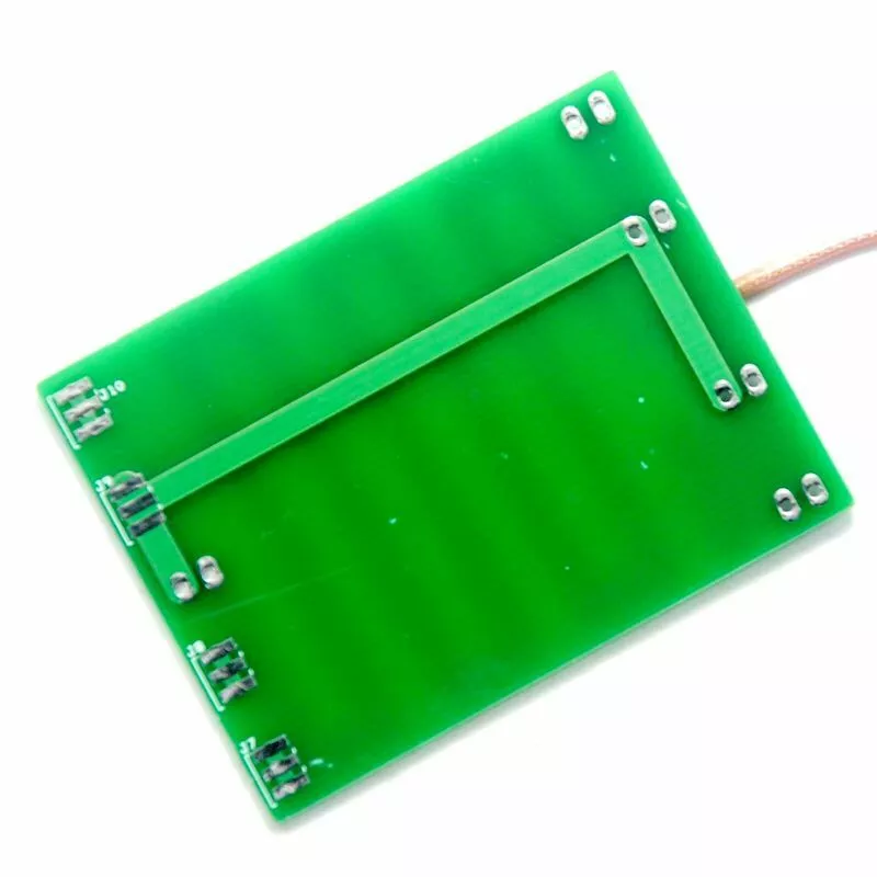
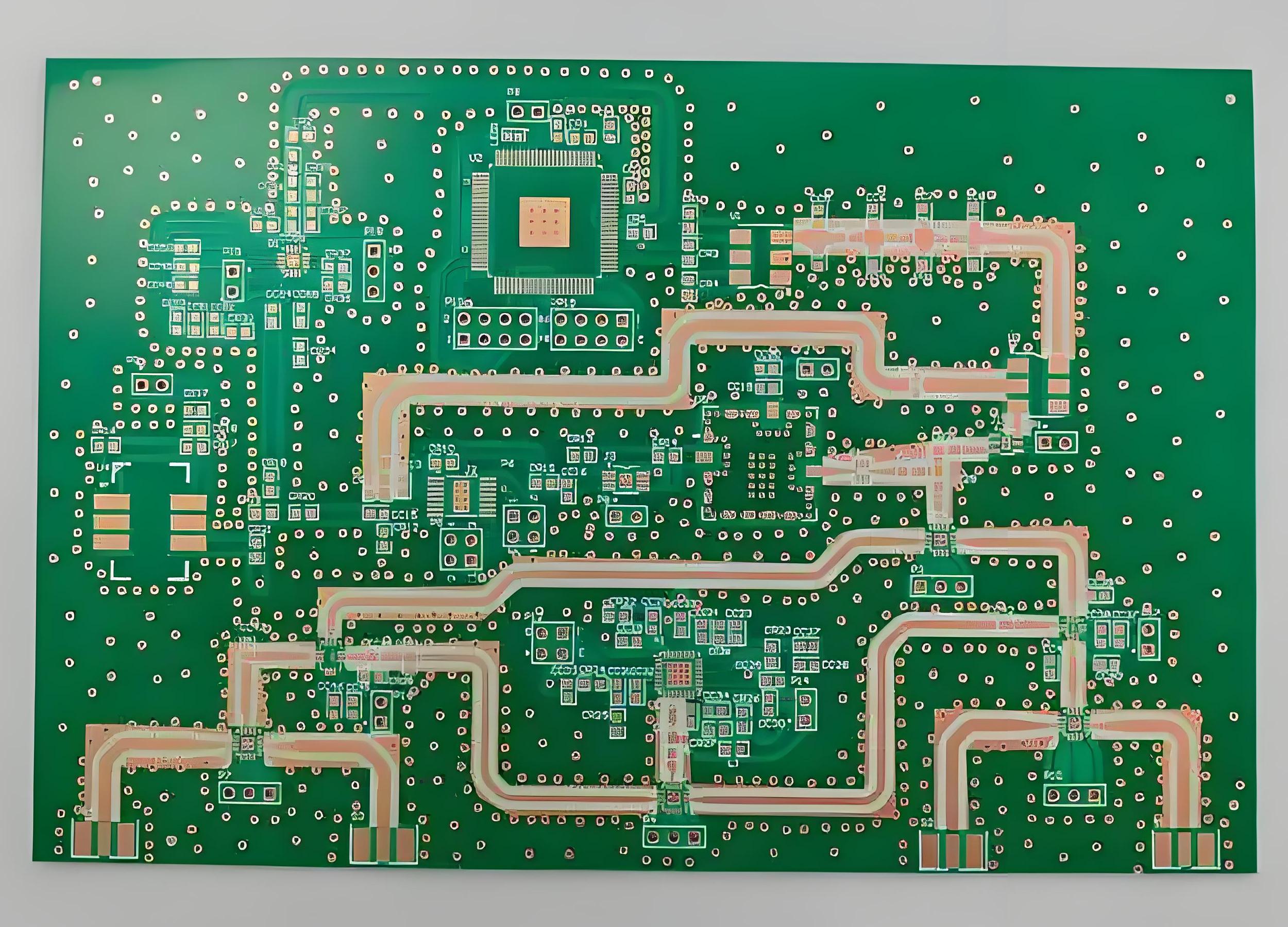
The most common color of PCB is green. Green PCB boards are the most common choice because they have good contrast, making the logos and tracking lines on the board clearly visible, while being less irritating to the eyes and having good recognition effects in production.

Characteristics and application scenarios of different color PCBs

  • Green PCBs: the most common and affordable, with good contrast, suitable for most applications.
  • White PCBs: look clean and neat in various environments, but easily hide traces and have poor contrast.
  • Yellow PCBs: once more common, but with poor contrast with traces and screen printing, they are now less used.
  • Blue PCB: has good screen printing contrast, often used for specific brands and products, but it is easy to produce scratches during the production process.
  • Red PCB: common in high-end communication equipment and military electronic products, with good thermal stability and weather resistance.
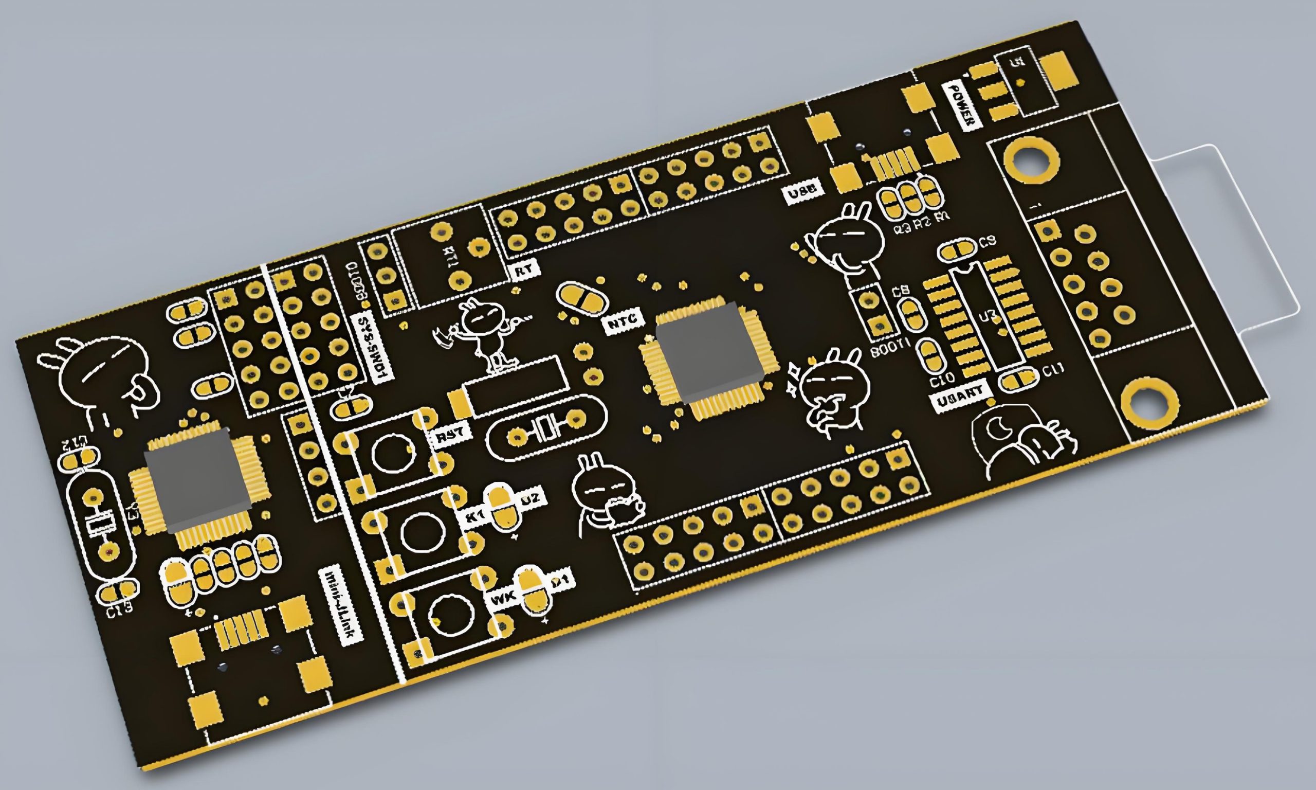
  • Black PCB: commonly used in high-end electronic products, such as computer motherboards, graphics cards, etc., but it is difficult to track details.

Reasons why green PCB is popular

  • Low cost: Green PCB is the most common in production, and factories usually have a large amount of green paint reserves, which is low cost.
  • Eye-friendly: Green is less irritating to the eyes and is not easy to get tired after long-term work.
  • Good contrast: The contrast between green PCB and white text is high, which enhances readability.

In short, black PCB has many advantages. Black solder mask has light shielding and good resolution. Its ingredients can resist electromagnetic interference, dissipate heat efficiently, and ensure stable operation of components. Different color PCBs are mainly due to different solder masks. Green is common, the process is mature, and the cost is low. It is mostly used in daily electronic products. Blue, yellow, etc. are both decorative and can be selected as needed, taking into account both electrical performance and appearance.

Ceramic Antenna vs PCB Antenna: Which Performs Better?

January 2nd, 2025

Ceramic Antenna vs PCB Antenna, both two are popular types of antennas that are used in electronic devices. While they both serve the same fundamental purpose, they have distinct characteristics that make them suitable for different applications. In the world of wireless communication, antennas play a crucial role in transmitting and receiving signals. In this blog, we will explore the differences between ceramic antennas and PCB antennas, their advantages, uses, and more.

What is a Ceramic Patch Antenna?

A ceramic patch antenna is another type of antenna that uses ceramic material as its substrate. These antennas are typically made from materials like zirconia, alumina, or other ceramic compounds that offer high dielectric properties. The ceramic material provides excellent performance, especially at higher frequencies, making it suitable for applications like GPS and satellite communication.

Ceramic patch antennas are designed with a patch (or conductor) on top of the ceramic material, which is usually mounted on a ground plane. These antennas are more robust and reliable than their PCB counterparts, especially when used in environments that require precision and high performance.

What is the Range of Ceramic Antenna?

Ceramic antennas are known for their excellent range, especially when used in GPS systems. Due to the high dielectric constant of ceramic materials, these antennas can transmit and receive signals over long distances with minimal loss. The range of a ceramic antenna depends on various factors, including the specific design, frequency, and environment in which it is used.

In general, ceramic antennas are effective for applications requiring longer-range communication, such as satellite communication, vehicle tracking, and high-performance wireless systems. Their ability to maintain a strong signal even at greater distances makes them ideal for outdoor and remote applications.

Why Are GPS Antennas Ceramic?

GPS antennas are commonly made from ceramic materials due to their superior dielectric properties. The ceramic material helps to maintain signal integrity, especially in environments with high levels of interference. GPS systems require precise, accurate signal reception, and ceramic antennas provide the reliability needed for such applications.

Additionally, ceramic antennas are compact and lightweight, which is essential for portable GPS devices like handheld GPS receivers and automotive navigation systems. Their ability to provide stable and consistent signal reception at various frequencies makes them the go-to choice for GPS technology.

How Does a Ceramic Antenna Work?

A ceramic antenna works by converting electrical signals into electromagnetic waves and vice versa. The process begins when an electrical current is passed through the antenna’s conductive elements, generating a fluctuating electromagnetic field. This electromagnetic field then radiates from the antenna in the form of radio waves.

In the case of a ceramic antenna, the high dielectric properties of the ceramic material enhance the efficiency of this process. The material helps to focus and direct the electromagnetic waves, allowing for better signal strength and range. Ceramic antennas are designed to operate at specific frequencies, and their performance is optimized to meet the requirements of various communication systems.

What is a PCB Antenna?

A PCB antenna is a type of antenna integrated into the PCB of an electronic device. These antennas are designed using the same materials and manufacturing processes used to produce the rest of the circuit board. PCB antennas are typically thin and can be designed in various shapes, depending on the needs of the device.

These antennas are often chosen for their low cost, ease of integration, and compact size. The simplicity of their design makes them suitable for a wide range of consumer electronics, including smartphones, tablets, laptops, and IoT devices.

What is a PCB Trace Antenna?

A PCB trace antenna is a specific type of PCB antenna, where the antenna’s design is embedded directly into the PCB as a copper trace. This design allows the antenna to be integrated seamlessly into the PCB without requiring additional components or external parts. PCB trace antennas are usually smaller, lightweight, and cost-effective, making them ideal for compact devices that require space-saving solutions.

They are commonly used in small form-factor devices, such as wireless routers, Bluetooth devices, and GPS receivers. Due to their simplicity, they are often chosen for consumer-grade products.

What are the Advantages of PCB Antenna?

PCB antennas offer several advantages that make them a popular choice in modern electronic devices. Here are some key benefits:

Compact Size: PCB antennas are integrated directly into the PCB, saving space within the device. This is crucial for compact and portable devices.

Cost-Effective: Since they are part of the PCB, the cost of manufacturing is lower than traditional antennas that require separate components or assembly processes.

Simplicity: PCB antennas are easy to design and integrate into existing PCB layouts. Their simplicity reduces the complexity of the overall design and assembly process.

Customization: PCB antennas can be customized to fit the specific needs of a device, with various shapes and sizes available to accommodate different designs.

Reliability: PCB antennas are highly reliable due to their integration into the PCB, making them resistant to external factors like environmental damage.

What are PCB Antennas Used For?

PCB antennas are used in a variety of applications, especially in devices where size and cost are critical factors. Some common uses include:

IoT Devices: PCB antennas are widely used in IoT devices such as smart home systems, sensors, and wearables. Their compact size and efficiency make them perfect for these types of devices.

Mobile Devices: Smartphones, tablets, and other portable electronics often incorporate PCB antennas due to their low-profile design and cost-effectiveness.

Wireless Communication Systems: PCB antennas are used in wireless routers, Bluetooth devices, and Wi-Fi systems for communication and signal transmission.

Consumer Electronics: From gaming consoles to digital cameras, many consumer electronic products rely on PCB antennas to support wireless capabilities.

In conclusion, both ceramic and PCB antennas have their own unique strengths and applications. Ceramic antennas excel in performance, range, and reliability, making them perfect for high-performance applications like GPS and satellite communication. PCB antennas, on the other hand, offer cost-effectiveness, compactness, and ease of integration, making them ideal for a wide range of consumer electronic devices and IoT systems.

The choice between ceramic and PCB antennas depends on the specific requirements of the device, including factors like size, cost, signal range, and performance. By understanding the differences between these two types of antennas, you can make an informed decision on which one best suits your needs.

For companies looking to explore the benefits of both antenna types, it’s important to work with a trusted manufacturer who can offer tailored solutions. At EBest Circuit (Best Technology), we provide high-quality Ceramic and PCB antennas’ components to meet the diverse needs of our customers. Whether you need a compact PCB antenna or a high-performance ceramic antenna, we have the expertise to help you achieve the best solution for your project.

What is pcb board assembly? PCB assembly manufacturer

January 2nd, 2025

What is pcb board assembly? PCB board assembly is the process of installing various electronic components (such as resistors, capacitors, chips, etc.) on the PCB and achieving electrical connections through welding and other methods to build a circuit board that can achieve specific electronic functions. This process includes component preparation, PCB board pretreatment, welding and post-assembly inspection.

What is the assembly of a PCB?

What is pcb board assembly? PCB assembly manufacturer

PCB assembly is the process of installing and electrically connecting various electronic components to a printed circuit board according to design requirements. It includes component preparation (purchase inspection, classified storage), PCB preparation (inspection, cleaning), welding (plug-in welding and patch welding) and post-assembly inspection (appearance and electrical performance inspection). Its quality is crucial to the performance and reliability of electronic products and is widely used in consumer electronics, industrial control, communications, automotive electronics and other fields.

How do you assemble a PCB board?

  • Component preparation: Purchase electronic components according to design documents and check whether the component specifications, models and appearance are qualified. After that, the qualified components are classified and stored by type, packaging form, etc.
  • PCB preparation: Check the appearance of the PCB board for scratches, short circuits and other defects, and wipe it with a special cleaner or alcohol to ensure that the surface is free of oil and dust, and that the pads are flat and free of oxidation.
  • Soldering process: Insert the component pins into the corresponding holes of the PCB, use an electric soldering iron to melt the solder to fill the pins and pads to form solder joints, and pay attention to controlling the temperature and time.
  • SMT soldering: Print solder paste on the PCB pads, place the components with a SMT machine, and then heat them according to the temperature curve through a reflow oven to melt the solder paste to form solder joints.
  • Post-assembly inspection: Perform an appearance inspection to check the solder joints and component installation. Then perform an electrical performance test, use professional equipment to check whether the function is normal, and troubleshoot and repair the faults.

What is the function of PCB assembly?

The main functions of PCB assembly include the following aspects:

  • Electrical connection: The copper wire tracks on the PCB board can connect various electronic components (such as resistors, capacitors, and integrated circuits) to form a complete circuit system. This efficient connection method simplifies circuit design and improves circuit reliability.
  • Component support: PCB provides stable support for components. Through welding and other methods, components can be firmly mounted on PCB, which improves the structural integrity and portability of the equipment.
What is pcb board assembly? PCB assembly manufacturer
  • Circuit protection: The insulating material of PCB can effectively isolate electromagnetic interference and protect the circuit from the external environment (such as moisture, dust, etc.), thereby extending the service life of electronic equipment, especially in harsh industrial environments.
  • Heat dissipation function: In high-performance, high-power electronic equipment, the metal layer (such as copper foil) on the PCB can quickly absorb and disperse the heat generated when the circuit is working, preventing components from being damaged by overheating. By optimizing the design, such as increasing the thickness and layout of the copper foil, the heat dissipation efficiency can be further improved.
  • Space optimization and compact structure: The design of the PCB is not only related to the functional realization of the circuit, but also affects the production cost, production efficiency and subsequent maintenance and replacement. Optimizing the use of space makes the internal structure of electronic equipment more compact and beautiful.

What is the standard for PCB assembly?

The standardization of PCB assembly is one of the important measures to ensure product quality and reliability. The following are the main standards for PCB assembly:

  • PCB board size and positioning: The size and positioning of the PCB board should meet the design requirements to ensure accurate alignment and fixation during the assembly process.
  • Component welding quality: The quality of the welding point is the key. The welding point should be smooth, firm, and burr-free to avoid poor welding, cold welding and other undesirable phenomena.
  • Component arrangement and layout: The arrangement and layout of the components should meet the design requirements to ensure the correct spacing and position between the components to avoid mutual interference.
  • Solder point quality: The solder joint should be firm, smooth, and burr-free to ensure the normal operation of the circuit.
  • Appearance quality: The surface of the PCB board should be clean, flat, and scratch-free, and the components should be arranged neatly and beautifully.
  • Electrical performance: Ensure that the electrical performance of the PCB after assembly meets the design requirements.
  • Weather resistance: PCB assembly should have good weather resistance and be able to work stably under different environmental conditions.
  • Reliability: The durability and reliability of the components should be considered during the assembly process to ensure stability in long-term use.

In addition, the specific assembly standards may vary depending on different application scenarios and product types. During the assembly process, relevant standards and requirements should be followed to ensure the quality and stability of the assembly.

What files are needed for PCB assembly?

The following main files are needed in the PCB assembly process:

  • Gerber file: This is the most critical file in PCB production, which contains the geometric information of each layer of the circuit board, such as copper lines, pads, solder mask and silk screen layers. Gerber files are usually generated by CAD software and saved in a standard format.
  • Drill file (.drl or .xin): This file provides the location and size information of all the drill holes on the circuit board, ensuring that the drill holes are accurately aligned with the circuit pattern.
  • Bill of Materials (BOM): The BOM lists all the materials and components that make up the circuit board, including their quantity, specifications and supplier information.
  • Coordinate files: These files provide the coordinate and orientation information of each component on the circuit board, which is essential for the automated assembly process.
  • Assembly drawings: If the PCB needs to be assembled with other electronic components, it is necessary to provide assembly drawings or assembly instructions, which detail how the components are installed on the circuit board.
  • Test requirements: If the manufacturer is required to perform specific tests, such as functional tests or electrical performance tests, it is necessary to provide test requirements or test instructions files.
  • Design Rule Check File (DRC): Used to verify whether the PCB design meets the manufacturing requirements and standards, helping to find and correct potential problems during the design stage.
  • 3D Model (STEP File): Used to generate a 3D model of the circuit board to help simulate and verify during the production process.
  • Structure Drawing (DXF format): Used to make a CAD structure drawing of the circuit board to ensure accuracy during the manufacturing process.

When providing these files, make sure they are up-to-date, accurate, and match the production requirements. It is also very important to maintain communication with the manufacturer to ensure that they have a clear understanding of the design requirements and can produce as expected.

What are the materials used in PCB assembly?

PCB assembly mainly uses the following materials:

1. Electronic components

  • Passive components: including resistors (used to control current and voltage, with a variety of resistance values, powers and packaging forms), capacitors (used to store charge and filter, there are ceramic, electrolytic, tantalum capacitors and other types, with different capacities and withstand voltage values), inductors (used to store magnetic field energy, with winding and stacked inductors, and the unit of inductance is Henry).
What is pcb board assembly? PCB assembly manufacturer
  • Active components: such as integrated circuits (including various functional circuits, with DIP, SOP, BGA and other packaging forms), transistors (used for amplification and switching functions, with BJT and FET and other types, with different parameters).

2. Welding materials

  • Solder wire: The main component is tin-lead or lead-free alloy, with different diameters, lead-containing solder wire has a lower melting point, lead-free solder wire has a higher melting point, and often contains flux inside.
  • Solder paste: used for SMT welding, it is a mixture of solder powder and flux, and its viscosity and metal content affect the quality of printing and welding.
  • Flux: used to remove metal surface oxides and reduce solder surface tension, available in liquid, paste and other forms, and ingredients include organic acids, rosin, etc.

3. PCB substrate materials

  • FR-4: Commonly used epoxy glass fiber cloth laminate, with good insulation, mechanical strength and thermal stability, and different thicknesses.
  • Ceramic substrate: excellent thermal conductivity and high-frequency performance, such as aluminum nitride and alumina ceramic substrates, suitable for high-power and high-frequency devices.
  • Flexible PCB substrate: used for bendable or foldable devices, the material is soft, and polyimide is often used as an insulating layer.

4. Other auxiliary materials

  • Cleaning agent: used to clean impurities on PCB boards, including alcohol and special electronic cleaning agents.
  • Thermal conductive materials: such as thermal grease and thermal conductive tape, used for heat dissipation of high-power components.

How is a PCB board structured?

The basic structure of a PCB board includes multiple layers, each of which has its specific functions and effects.

PCB boards are mainly composed of the following layers:

  • Top Layer: This is the top layer of the PCB board, which is usually filled with electronic components such as resistors, capacitors, and chips. The top layer not only carries these components, but also is responsible for their connection and wiring to ensure that current and signals can be accurately transmitted.
  • Bottom Layer: Located at the bottom of the PCB board, it is mainly responsible for the laying of ground wires and the connection of auxiliary signal lines. The bottom layer provides a solid support for the circuit board to ensure the stability and safety of the circuit.
  • Inner Layer: Located between the top layer and the bottom layer, it is composed of multiple layers of copper foil stacked to form a complex circuit network. The inner layer is used to conduct signals and power supply, reduce signal interference, and ensure the clarity and accuracy of the signal.
  • Solder Mask Layer: This is a special layer, the main function of which is to protect the pads on the circuit board, prevent the solder from splashing into other areas during the soldering process, and ensure the soldering quality and stability of the circuit.

What is the difference between PCB and PCB assembly?

The main difference between PCB and PCBA lies in their status and function.

1. Definition and function

  • PCB: PCB is the cornerstone of electronic devices, providing physical support and electrical connection for electronic components. It consists of a conductive copper layer and an insulating layer, and is usually manufactured by methods such as chemical etching. The PCB itself does not contain any electronic components, but is just an empty circuit board.
What is pcb board assembly? PCB assembly manufacturer
  • PCBA: Printed circuit board assembly refers to the installation of electronic components on the PCB to form a complete circuit. PCBA is functional and can be directly installed in the final product for use.

2. Cost and complexity

  • PCB: Since there are no electronic components, the manufacturing process is relatively simple and the cost is low.
  • PCBA: Due to the need to install and test electronic components, the manufacturing process is more complicated and the cost is higher. PCBA is more complex and more expensive than PCB.

3. Application

  • PCB: Mainly used to manufacture PCBA, as a support and connection frame for electronic components.
  • PCBA: After assembly, PCBA is used in various electronic devices such as computers, smartphones, home appliances, etc.

In summary, PCB board assembly is an interlocking, delicate and complex process. From the careful selection of component preparation, to the pretreatment of PCB boards, and the final strict control, each step should not be underestimated. It organically integrates various electronic components with PCB boards to become PCBA.

What Do You Know About Aluminum PCB Prototyping?

January 2nd, 2025

Aluminum PCB prototyping has transformed how electronic designs are tested and refined. It offers a reliable way to create high-performance circuits with enhanced thermal management and durability. Whether you’re developing a small batch for testing or a custom design for specific needs, understanding aluminum PCB prototyping is essential. At EBest Circuit (Best Technology), we specialize in offering tailored aluminum PCB solutions with fast delivery and exceptional quality.

What Is an Aluminum PCB?

An aluminum PCB is a type of printed circuit board with an aluminum core, which acts as a heat sink. This design improves heat dissipation, making it ideal for high-power applications like LED lighting and automotive systems. Its structure includes an aluminum base, an insulating layer, and copper traces. This combination ensures excellent thermal performance and reliability, especially in demanding environments.

What Is PCB Prototyping?

PCB prototyping is the process of creating a preliminary version of a printed circuit board to test its functionality and design. It allows engineers to identify and correct potential flaws before full-scale production. With advancements in technology, prototyping has become faster and more cost-effective, enabling quick iterations for design improvements.

What Is ASIC Prototyping?

ASIC (Application-Specific Integrated Circuit) prototyping involves creating a functional model of a custom-designed chip. While not directly related to PCBs, it shares similarities in testing and refining designs before mass production. Combining ASIC prototyping with aluminum PCB prototyping can optimize performance in high-frequency or power-intensive applications.

How Much Does a PCB Prototype Cost?

The cost of a PCB prototype depends on several factors, including material, complexity, size, and quantity. Aluminum PCB prototypes are generally more expensive than standard FR4 prototypes due to the specialized materials and processes involved. However, their benefits in thermal management and durability often outweigh the higher initial cost. At EBest Circuit (Best Technology), we offer competitive pricing for small and large-scale prototypes, ensuring value without compromising quality.

How to Make PCB Prototyping?

PCB prototyping involves several steps:

Designing the Circuit: Engineers create a detailed schematic using design software.

Fabrication: The design is transferred onto the aluminum base through processes like etching and drilling.

Assembly: Components are soldered onto the board.

Testing: The prototype undergoes rigorous testing to verify performance.

Advanced tools and precise manufacturing are critical to ensuring the prototype matches the design requirements.

How Do You Make a Circuit with Aluminum Foil?

Creating a simple circuit with aluminum foil is a basic DIY project often used for educational purposes. Aluminum foil serves as the conductive path for electricity. While this method is not suitable for professional applications, it demonstrates the principles of electrical circuits. For real-world use, aluminum PCBs provide far superior performance and reliability.

How Do You Make Aluminum PCB?

Manufacturing an aluminum PCB involves:

Material Preparation: Selecting a high-quality aluminum core.

Lamination: Adding an insulating layer and copper foil.

Patterning: Using photolithography to create the circuit pattern.

Etching: Removing excess copper to form the traces.

Drilling and Plating: Creating holes and coating them with conductive material.

Each step requires precision to ensure the PCB meets technical and thermal specifications.

What Are the Advantages of Aluminum PCB?

Aluminum PCBs are known for their thermal conductivity, durability, and environmental friendliness. They effectively dissipate heat, reducing the risk of component failure. Their robust structure ensures longevity, even in harsh conditions. Additionally, aluminum is recyclable, making these PCBs an eco-conscious choice. With these benefits, aluminum PCBs are widely used in LED lighting, automotive systems, and power electronics.

Why Choose EBest Circuit (Best Technology)?

EBest Circuit (Best Technology) stands out for offering a wide range of products, small quantity orders, and high-quality standards. Our expertise in aluminum PCB prototyping ensures fast delivery and fully customized solutions. We prioritize customer satisfaction by delivering exceptional service and reliable results.

In Conclusion, aluminum PCB prototyping bridges the gap between innovative design and practical application. Its ability to combine thermal performance with reliability makes it a top choice for modern electronics. At EBest Circuit (Best Technology), we are dedicated to supporting your prototyping needs with superior quality and customized solutions. Trust us for your next project, and experience the Best in PCB manufacturing.

What temp does pc board solder melt? Desoldering temperature

December 31st, 2024

What temp does pc board solder melt? Solder melting points vary depending on the type. Traditional tin-lead solder, the common 63/37 tin-lead alloy melts at about 183°C. Today’s widely used lead-free solder, for example, tin-silver-copper alloy, melts at about 217°C – 227°C. When soldering SMD components, the temperature is set at around 240°C – 260°C to ensure that the tin-silver-copper solder is fully melted.

What temperature do PCBs melt?

The melting point of the PCB substrate itself is usually between 130°C and 140°C. This means that above this temperature range, the FR-4 substrate may begin to soften and melt.

What temp does pc board solder melt? Desoldering temperature

In electronics manufacturing, components on PCB substrates are usually connected by soldering technology. The solder used in the soldering process has a lower melting point, generally between 183°C and 215°C. This ensures that during the soldering process, the solder can melt and form a reliable connection with the PCB substrate and components.

What is the best solder for circuit boards?

The best solder selection for circuit boards depends on the specific application requirements and environmental conditions.

  • Tin-lead solder wire: Tin-lead solder wire is one of the most commonly used solders in circuit board soldering. It is usually made of 63/37 tin-lead alloy, which has the advantages of low melting point, good fluidity and easy operation.
  • Lead-free solder wire: With the improvement of environmental awareness, lead-free solder wire has gradually become the mainstream. Lead-free solder wire is mainly composed of tin, silver, copper and other elements, and has the characteristics of high melting point, high hardness and wear resistance.
  • Silver paste: Silver paste is a packaging material widely used in high-frequency circuits, microwave circuits, power devices and printed circuit boards. It is applied to the surface of the circuit board by spraying or printing, and is baked and cured at high temperature.

What is the melting point of circuit board solder?

The melting point of circuit board solder is usually between 183℃ and 214℃. Commonly used solder is tin-copper alloy, which has good plasticity, conductivity and corrosion resistance, making it the most commonly used soldering material. In addition, the melting point of lead solder is 183℃, while the melting point of lead-free solder is 217℃.

In the actual soldering process, the soldering temperature is usually about 50℃ higher than the melting point of the solder, so the actual soldering temperature is generally between 220℃ and 250℃.

What temp does pc board solder melt? Desoldering temperature

For manual soldering, the soldering temperature is generally between 300℃ and 350℃ to ensure that the solder wire melts quickly and ensures good wettability. For wave soldering, the optimal temperature is 280℃, and the tin furnace temperature can be set to 288±5℃.

What temperature does 50/50 solder melt at?

The melting temperature range of 50/50 solder is 190℃ to 216℃. This solder is an alloy composed of 50% tin and 50% lead, and its melting temperature is approximately in this range.

In addition, the melting point of solder varies depending on the composition. For example, the melting points of lead solder wire are as follows:

  • 63/37 melting point is 183℃
  • 60/40 melting point is 185℃ to 190℃
  • 55/45 melting point is 187℃ to 202℃
  • 50/50 melting point is 190℃ to 216℃
  • 45/55 melting point is 192℃ to 227℃
  • 40/60 melting point is 194℃ to 238℃
  • 35/65 melting point is 198℃ to 247℃
  • 30/70 melting point is 202℃ to 256℃.

Can you burn a PCB while soldering?

The PCB may be burned during soldering, which mainly depends on the control of soldering methods and parameters.

The main reasons for burning PCB during laser welding include:

  • Excessive laser power: Laser power is a key factor in determining the heat input of welding. If the power is set too high, the laser energy will be concentrated in the solder joint in a short time, and the heat generated will far exceed the heat required for the solder to melt, causing PCB burns.
  • Improper pulse width and frequency: The laser pulse width and frequency will also affect the welding effect. A pulse width that is too long or a frequency that is too high will cause excessive heat accumulation, and the heat transferred to the PCB board will increase, which may cause burns.
What temp does pc board solder melt? Desoldering temperature
  • Poor thermal performance of materials: PCB materials have low thermal conductivity or small specific heat capacity, and the heat conduction speed inside the material is slow, which is easy to concentrate near the solder joint, causing local overheating and burns.
  • Surface treatment and quality problems: When a PCB board with oil, oxide layer or impurities on the surface is irradiated by laser, the contaminants will absorb part of the laser energy, generate additional heat, and increase the risk of burns.

The reasons for burning PCBs during traditional welding include:

  • Excessive welding temperature and excessive welding time: The temperature generated during welding is indeed very high, but if the welding temperature is too high or the welding time is too long, it may cause damage to the components on the circuit board or thermal cracks in the circuit board itself.

Measures to avoid burning PCB

  • Choose appropriate welding tools and methods: Choose welding tools that suit your needs and control welding temperature and time. For laser welding, reasonably set the laser power, pulse width and frequency to ensure that the heat input is within a safe range.
  • Control welding temperature and time: Set the appropriate welding temperature according to the material of the circuit board and the heat resistance of the components, and try to shorten the welding time.
  • Optimize welding skills: Master welding skills to avoid the problems of thermal expansion deformation of copper foil and separation of copper foil from the substrate caused by high-energy local rapid heating.
  • Check the quality of PCB boards: Ensure that the surface treatment of PCB boards is clean, without oil, oxide layer or impurities, and avoid contaminants absorbing laser energy to generate additional heat.

What temperature does PCB solder reflow at?

The temperature range of PCB solder during reflow soldering is usually 220℃ to 249℃. During the reflow soldering process, the solder paste needs to undergo processes such as solvent volatilization, flux removal of oxides on the surface of the weldment, solder paste melting, reflow, and solder paste cooling and solidification. The specific temperature zones are as follows:

  • Preheating zone: The temperature gradually rises from room temperature to about 150℃. At this stage, the solvent and gas in the solder paste begin to evaporate, the flux wets the pads and component pins, and the softened solder paste covers the pads, isolating oxygen and preparing for the next welding.
What temp does pc board solder melt? Desoldering temperature
  • Constant temperature zone: The temperature is between 150℃ and 200℃, ensuring that the PCB and components are fully preheated to avoid damage to the PCB and components due to a sudden temperature rise.
  • Reflow zone: The temperature rises rapidly to 220℃, up to 249℃. In this area, the solder paste reaches a molten state, the liquid solder wets and diffuses, and forms solder joints between the pads, component ends and pins.
  • Cooling zone: The solder joints gradually solidify, completing the entire reflow process.

Temperature control during reflow is extremely important because it directly affects the welding quality and product reliability. Too high or too low temperature may cause welding defects such as solder balls, cold soldering, bridging and other problems.

What temperature should pcb be desoldered at?

The temperature range of PCB during desoldering is generally between 250℃ and 350℃. The specific temperature should be adjusted according to the size and type of components on the circuit board. For smaller components and thin lines, the temperature should be set at around 250℃; for larger components and thicker solder joints, the temperature can be set at around 350℃.

Specific temperature requirements for different welding methods

  • Manual welding: usually set between 300℃ and 350℃. For precision components such as IC and SMD, it is recommended to control between 260℃ and 300℃; for welding of large-area heat sinks or power lines, the temperature may need to be increased to around 380℃.
  • Wave soldering: The temperature of the preheating zone is usually 90℃ to 140℃, and the temperature of the solder tank is 240℃ to 260℃.
  • Reflow soldering: The temperature of the preheating zone is 150℃ to 200℃, the wetting zone is maintained at 150℃ to 200℃, the temperature of the reflow zone is 230℃ to 260℃, and the temperature of the cooling zone drops rapidly to below 100℃.
  • Laser welding: The local temperature is usually 250℃ to 300℃, and the exposure time is usually 0.1 to 2 seconds.

In short, the melting point of printed circuit board solder varies depending on the type and application scenario. Among traditional tin-lead solders, the melting point of 63/37 tin-lead alloy is about 183℃, which was widely used in PCB welding. With the demand for environmental protection, lead-free solder has emerged, and the melting point of common tin-silver-copper alloy is 217℃ – 227℃.

Ceramic Base PCB, Reliable Ceramic Base PCB Manufacturer

December 31st, 2024

Ceramic base PCB is gaining popularity due to their exceptional performance in challenging environments. As a leading ceramic base PCB manufacturer, EBest Circuit (Best Technology) takes pride in offering top-quality solutions for a wide range of applications. This blog explores ceramic base PCBs, their benefits, applications, types, materials, design considerations, and why EBest Circuit (Best Technology) stands out as the ideal partner for your PCB needs.

What Is Ceramic Base PCB?

A ceramic base PCB uses ceramic materials as its substrate instead of traditional options like FR4. These PCBs are renowned for their excellent thermal conductivity, electrical insulation, and mechanical stability. Designed for high-performance applications, they excel in environments requiring durability and precision.

Ceramic base PCB is often chosen for industries like aerospace, automotive, and medical devices, where reliability and efficiency are paramount. Its unique properties make them indispensable for cutting-edge technologies.

What Are The Benefits of Ceramic Base PCB?

Ceramic base PCBs offer several advantages that set them apart from conventional options. Their high thermal conductivity ensures efficient heat dissipation, making them ideal for power-intensive devices. Their low coefficient of thermal expansion minimizes the risk of mechanical stress, ensuring long-lasting performance.

These PCBs are also highly resistant to chemical and environmental damage. Their excellent electrical insulation supports stable and reliable operations, even under challenging conditions. Combined with their compact size and lightweight nature, ceramic base PCBs are a top choice for innovative and efficient electronic designs.

What Are The Applications of Ceramic Base PCBs?

Ceramic base PCBs find applications across various industries due to their superior properties. In the automotive sector, they are used in engine control systems and LED lighting. Aerospace applications include navigation systems and avionics, where reliability is critical.

In the medical field, ceramic base PCBs are essential for diagnostic devices, imaging systems, and surgical instruments. They are also widely employed in telecommunications for RF and microwave components. Consumer electronics, including LED displays and sensors, further benefit from their durability and efficiency.

What Are The Different Types of Ceramic Base PCB?

Ceramic base PCBs are available in several types, each designed to meet specific requirements:

Aluminum Nitride (AlN) PCBs: Known for high thermal conductivity and excellent electrical insulation.

Alumina (Al2O3) PCBs: Cost-effective and suitable for a wide range of applications.

Beryllium Oxide (BeO) PCBs: Exceptional thermal performance, though less commonly used due to safety concerns.

Silicon Nitride (Si3N4) PCBs: High strength and thermal shock resistance, ideal for demanding environments.

Each type offers unique features to suit different industries and applications.

Why Turn To EBest Circuit (Best Technology) For Ceramic Base PCB?

EBest Circuit (Best Technology) is a trusted name in the PCB manufacturing industry, offering unmatched expertise in ceramic base PCBs. We cater to diverse customer needs with our wide product range, including various types of ceramic PCBs. Whether you require small quantities or bulk orders, our flexible production capabilities ensure your demands are met efficiently.

Our focus on quality is unwavering. Every product undergoes stringent testing to meet the highest standards. We prioritize fast delivery, ensuring your projects stay on schedule. With our customization services, you can rely on us for tailored solutions that fit your specific requirements. Our commitment to exceptional service makes us the preferred choice for customers worldwide.

What Is the Material of Ceramic Base PCB?

The materials used in ceramic base PCBs are critical to their performance. Common materials include:

Aluminum Nitride (AlN): Offers outstanding thermal conductivity and is ideal for high-power applications.

Alumina (Al2O3): Provides a balance of performance and cost-effectiveness, making it widely popular.

Beryllium Oxide (BeO): Delivers superior thermal performance but requires careful handling.

Silicon Nitride (Si3N4): Combines strength, thermal resistance, and reliability.

These materials are chosen based on application requirements, ensuring optimal performance and durability.

How To Design Ceramic Base PCB?

Designing ceramic base PCBs requires careful consideration of material properties, thermal management, and circuit layout. The substrate’s thermal conductivity must align with the application’s heat dissipation needs. Selecting appropriate components and ensuring proper spacing is essential for reliable operation.

Advanced fabrication techniques, such as laser drilling and metallization, are used to achieve precision and quality. Working with experienced manufacturers like EBest Circuit (Best Technology) ensures that every aspect of your design is optimized for performance and longevity.

FAQs About Ceramic Base PCB

1. What industries use ceramic base PCBs?

Industries like automotive, aerospace, medical devices, telecommunications, and consumer electronics widely use ceramic base PCBs.

2. How does ceramic base PCB compare to traditional PCBs?

Ceramic base PCBs offer superior thermal conductivity, mechanical strength, and environmental resistance compared to traditional PCBs.

3. Can ceramic base PCBs be customized?

Yes, EBest Circuit (Best Technology) provides fully customized ceramic base PCBs to meet unique application requirements.

4. What is the lead time for ceramic base PCBs?

With our fast delivery services, lead times are minimized, ensuring your projects stay on track. Normally, The fastest lead time is about 2 weeks.

5. Why is thermal conductivity important in ceramic base PCBs?

High thermal conductivity ensures efficient heat dissipation, critical for maintaining performance in high-power applications.

In short, ceramic base PCBs are indispensable for industries requiring high performance and reliability. EBest Circuit (Best Technology) excels in delivering top-notch ceramic base PCBs tailored to your needs. With our diverse product range, exceptional quality, and fast delivery, we are your trusted partner for ceramic base PCB solutions. If you have any questions or any inquiry about ceramic base PCB products, warm welcome to consult us via sales@bestpcbs.com. Thank you.

Aluminum PCB LED, Aluminum Base PCBs for LEDs

December 31st, 2024

An aluminum PCB LED refers to a specialized printed circuit board (PCB) that uses an aluminum base to support and enhance LED (Light Emitting Diode) applications. These PCBs are specifically designed to manage the heat generated by LEDs during operation. In essence, an aluminum PCB LED combines the benefits of advanced circuit design with excellent thermal conductivity, ensuring optimal performance for LED systems.

Aluminum PCBs have revolutionized LED lighting by addressing heat dissipation challenges. These circuit boards, crafted with an aluminum base, deliver excellent thermal management, durability, and efficiency. This blog explores their material composition, thermal properties, and significance in LED applications. Whether you’re designing LED systems or curious about the advantages of aluminum PCBs, this comprehensive guide offers valuable insights.

What Is the LED of Aluminum?

LEDs mounted on aluminum PCBs are essential for applications demanding high efficiency and longevity. The aluminum base acts as a thermal conductor, transferring heat away from the LED components. This process enhances the lifespan and performance of LEDs, particularly in high-power applications like floodlights and automotive lighting. These PCBs are also lightweight, making them suitable for compact designs.

What Is the Material of Aluminum PCB?

Aluminum PCBs typically consist of three layers:

1. Base Layer: Made of aluminum, this layer provides structural support and excellent heat dissipation.

2. Dielectric Layer: Positioned between the base and the circuit layer, it ensures electrical insulation while conducting heat.

3. Circuit Layer: Copper circuits are etched onto this layer to form the electrical connections.

The combination of aluminum and copper enhances conductivity and thermal efficiency. These materials make aluminum PCBs reliable for LED applications.

What Temperature Can Aluminum PCB Withstand?

Aluminum PCBs are designed to operate in high-temperature environments. They can typically withstand temperatures between 120°C and 150°C, depending on the design and material quality. High thermal resistance ensures consistent performance, even in demanding applications like outdoor LED lighting and automotive headlights. Selecting the right PCB thickness and dielectric material is critical for optimizing thermal tolerance.

What Is the Thermal Resistance of Aluminum PCB?

The thermal resistance of an aluminum PCB is the measure of its heat transfer capability. It typically ranges between 1.0°C/W and 2.0°C/W, depending on the board’s structure and material quality. Lower thermal resistance indicates better heat dissipation, which is essential for high-power LEDs. Aluminum PCBs achieve this through their unique combination of metal cores and dielectric materials.

How Thick Is Aluminum PCB?

Aluminum PCBs vary in thickness to suit different applications. Common thicknesses include:

Base Layer: Typically 1.0mm to 2.0mm.

Dielectric Layer: Around 0.075mm to 0.15mm.

Circuit Layer: Common circuit layer thickness is about 0.035mm‌.

The choice of thickness depends on the required mechanical strength, heat dissipation, and electrical load. Thicker boards are ideal for heavy-duty applications like industrial LED lighting.

What Is the Difference Between Copper and Aluminum PCB?

Copper and aluminum PCBs serve similar purposes but have distinct characteristics:

Thermal Conductivity: Copper PCBs offer higher conductivity, while aluminum PCBs balance thermal performance and cost.

Weight: Aluminum PCBs are lighter, making them ideal for compact designs.

Cost: Aluminum PCBs are generally more affordable than copper-based alternatives.

Aluminum PCBs are preferred for LED applications due to their efficient heat dissipation and lower production costs.

How Do You Connect LED to PCB?

Connecting LEDs to aluminum PCBs involves precise soldering. Here’s a simplified process:

1. Prepare the PCB: Clean the board and check the circuit layout.

2. Place the LED: Align the LED pins with the PCB pads.

3. Solder the Connections: Use a soldering iron to secure the LED.

4. Test the Circuit: Verify functionality with a power supply.

Aluminum PCBs are designed to handle heat generated during soldering, ensuring durability and reliable connections.

Why Use Aluminum PCB?

Aluminum PCBs are preferred for LED applications due to several reasons:

1. Heat Management: They efficiently dissipate heat, ensuring LEDs operate at optimal temperatures.

2. Durability: Aluminum provides structural strength and resistance to wear.

3. Lightweight: The boards are easy to integrate into compact devices.

4. Energy Efficiency: They reduce thermal losses, improving overall efficiency.

These features make aluminum PCBs a cornerstone in modern LED lighting solutions, from consumer electronics to industrial systems. EBest Circuit (Best Technology)’s competitive edge lies in its ability to deliver multiple types of products, customized to your needs, with fast delivery and unmatched quality.

What are Applications of Aluminum PCBs in LEDs?

Aluminum PCBs (Printed Circuit Boards) are widely used in LED applications due to their excellent thermal management properties. Here are the main applications of aluminum PCBs in LEDs:

1. High-Power LED Lighting: Aluminum PCBs are ideal for high-power LED lighting systems, such as streetlights, floodlights, and spotlights. The metal core provides effective heat dissipation, preventing LEDs from overheating and improving their efficiency and lifespan.

2. LED Modules for Displays: Aluminum PCBs are used in LED modules for large-scale digital displays, such as billboards and signage. The thermal management capacity of aluminum ensures the stability of the LEDs during continuous operation.

3. Automotive Lighting: In automotive lighting systems, aluminum PCBs are used for headlights, tail lights, and interior lighting. The ability of aluminum to manage heat is critical to maintain LED performance and prevent failure in harsh automotive environments.

4. Backlighting for LCD Displays: Aluminum PCBs are used in the backlight systems of LCD displays, such as those in TVs, monitors, and smartphones. The heat dissipation capabilities enhance the longevity and reliability of the LEDs used for backlighting.

In each of these applications, aluminum PCBs help to reduce the risk of overheating, enhance the performance of LEDs, and extend their operational life, making them a preferred choice for various LED-based lighting and display systems.

In conclusion, aluminum PCBs are indispensable for high-performance LED applications. Their superior thermal management, lightweight construction, and cost-effectiveness provide unparalleled benefits. Choosing the right aluminum PCB for your LED projects ensures durability and efficiency. If you need customized solutions, EBest Circuit (Best Technology) offers premium aluminum PCB led tailored to your requirements. Just feel free to contact us via sales@bestpcbs.com.

What is the soldering temperature of PCB? soldering temperature 60/40

December 30th, 2024

What is the soldering temperature of PCB?When using traditional tin-lead solder, the soldering temperature is roughly in the range of 183℃ – 327℃. For common tin-silver-copper alloys, the melting point is usually in the range of 217℃ – 227℃. During the soldering operation, the temperature is mostly controlled at around 250℃ – 300℃ to ensure that the solder is fully melted and a high-quality solder joint is formed.

What is the best temperature to solder at?

The optimal temperature range for PCB soldering varies depending on the soldering method.

soldering temperature
  • Surface mount technology: For surface mount technology (SMT), the soldering temperature is generally between 200-240 degrees Celsius. This soldering method includes hot air ovens and reflow soldering, which is mainly used in modern electronic equipment manufacturing.
  • Wave soldering: The soldering temperature of wave soldering is generally between 230-260 degrees Celsius. The preheating zone temperature of the wave soldering machine is usually 90-130℃, the solder temperature is 275℃~300℃, the immersion speed is 20mm/s~25mm/s, and the immersion time is 1s~3s.
  • Manual soldering: The temperature requirements for manual soldering are relatively high, usually set between 300℃ – 350℃. For precision components such as IC and SMD, it is recommended to control it at 260℃ – 300℃.
  • Reflow soldering: The preheating zone temperature of reflow soldering is heated from room temperature to 150℃ – 200℃, the wetting zone is maintained at 150℃ – 200℃, and the peak temperature of the reflow zone is 230℃ – 260℃. The entire reflow soldering process is usually controlled within 4-7 minutes.
  • Lead-free solder: For lead-free solder, due to its high melting point, the soldering temperature usually needs to be higher, generally between 250℃ – 280℃.

What temperature is 60 40 soldering?

The optimal soldering temperature range of 60/40 solder wire is 220℃-240℃. Within this temperature range, the fluidity and wettability of the solder wire are good, which can ensure the quality and effect of soldering components.

In addition, different types of solder wire have different optimal temperature ranges:

  • 63/37 alloy: high melting point, suitable for soldering circuits and PCB boards, the optimal temperature range is 260℃-280℃.
  • 55/45 alloy: melting point is 187℃-202℃, suitable for specific application scenarios.
  • 50/50 alloy: melting point is 190℃-216℃, suitable for soldering tasks requiring higher melting points.
  • 45/55 alloy: melting point is 192℃-227℃, suitable for soldering tasks requiring higher melting points.
  • 40/60 alloy: melting point is 194℃-238℃, suitable for specific high melting point soldering needs.
  • 35/65 alloy: melting point is 198℃-247℃, suitable for high melting point welding tasks.
  • 30/70 alloy: melting point is 202℃-256℃, suitable for extremely high melting point welding tasks.

What is too much heat on solder?

Overheating of PCB solder can lead to a variety of problems, including reduced soldering quality, component damage and safety hazards. Specifically:

  • Degraded soldering quality: Overheating can lead to increased solder fluidity, which may cause excessive solder joints or solder accumulation, affecting soldering quality. In addition, overheating may also cause solder joints to turn white, have no metallic luster, have a rough surface, easily peel off, and reduce strength.
soldering temperature
  • Component damage: High temperature accelerates the aging process of electronic components and shortens their life. Long-term overheating may cause damage, burning or failure of electronic components, requiring more frequent component replacement, and increasing repair and maintenance costs.
  • Safety hazards: Overheating may cause fire risks. In extreme cases, overheated PCB boards may cause wires, cables and other materials to melt, causing fires.

Do and don’ts of soldering?

The precautions for PCB soldering include the following aspects:

1. Selection of soldering materials and flux:

  • Soldering materials: Commonly used soldering materials include tin-lead solder, which is suitable for general electronic product assembly due to its low melting point, high mechanical strength, low surface tension, and good oxidation resistance.
  • Flux: Flux is divided into solder resist and soldering flux. The soldering flux is mainly used to remove oxide film, prevent oxidation, reduce surface tension, and increase solder fluidity. Commonly used soldering fluxes include rosin series, which are non-corrosive and suitable for electronic assembly soldering.

2. Key points of welding technology:

  • Surface treatment of weldment: Remove rust, oil, dust and other impurities on the welding surface.
  • Pre-soldering: Pre-moisten the welding parts of component leads or wires with solder to reduce welding errors.
  • Appropriate amount of flux: Rosin water should only wet the solder joints to be formed to avoid excessive use resulting in excessive solder joints or cold solder joints.
  • Keep the soldering tip clean: The soldering tip needs to be cleaned regularly to prevent oxidation from affecting the heating effect.

3. Control of welding temperature and time:

  • Temperature control: Too high or too low temperature of the soldering iron will affect the welding quality. It is recommended to use a white light adjustable soldering iron, the temperature is about 350°C for lead soldering, and the temperature is about 380°C for lead-free soldering.
  • Time control: Select the appropriate heat and time according to the size and shape of the solder joint to ensure the full melting of the solder and the activation of the active flux.

4. Soldering sequence and component placement:

  • Soldering sequence: Prioritize soldering of smaller components, such as resistors and capacitors, and finally solder larger components and connectors.
  • Component placement: Components should be neatly, centered, and placed on the board surface, and pay attention to the polarity of the components.

5. Ventilation and safety measures:

  • Ventilation: Harmful gases will be generated during welding, and exhaust fans or other ventilation equipment must be equipped.
  • Safe operation: Ensure the safety of the operating process, circuit boards and welding tools, and use anti-static tools and protective measures.

What temperature does solder reflow at?

The reflow temperature range of solder during reflow soldering is usually between 220-260℃. Specifically, the four key temperature zones of reflow soldering and their temperatures and times are as follows:

  • Preheating zone: The temperature is usually set at 150-200℃ for 60-120 seconds. The purpose of this stage is to preheat the circuit board and components to reduce thermal stress and avoid thermal shock.
  • Wetting zone: The temperature range is 180-230℃ for 30-90 seconds. At this stage, the solder paste begins to melt and penetrate into the solder joints, preparing for the next reflow stage.
soldering temperature
  • Reflow zone: The temperature is usually 220-260℃ for 30-60 seconds. At this stage, the solder paste is completely melted to form a stable solder joint. Too high a temperature or too long a time may cause the solder joint to overheat, while too low or too short a time may cause the solder joint to be loose.
  • Cooling zone: The temperature drops below 70℃ for 60-120 seconds. The rapid cooling process helps to reduce the thermal stress of the solder joints and improve the reliability and stability of the product.

In addition, the solder paste will go through four stages during the reflow process: solvent volatilization, oxide removal, melting and reflow, and cooling and solidification. The temperature and time settings of these stages are crucial to ensure the quality of welding and product reliability.

How to remove old solder?

There are mainly the following ways to remove old solder:

  • Use a solder sucker: The solder sucker is a commonly used tool, especially suitable for soldering work on precision circuits. When using a solder sucker, first heat the soldering iron to melt the solder joint, then gently place the solder sucker on the solder joint, and the molten solder will be absorbed by the solder sucker.
  • Use anhydrous ethanol or alcohol above 95%: Dip anhydrous ethanol or high-concentration alcohol on a soft brush, brush the solder joint, and then dry it with absorbent cotton.
  • Ultrasonic cleaning: Ultrasonic cleaning uses the high-frequency oscillation of ultrasound to produce a cavitation effect, which removes the dirt on the solder joint and accelerates the dissolution process of the cleaning fluid.
soldering temperature
  • Manual cleaning: Use manual tools such as tweezers, scrapers, etc. to directly clean the residual solder on the solder joint. This method is simple but inefficient, and it is easy to damage solder joints and components.
  • Use special tools: such as desoldering mesh wire, desoldering braided belt, etc. Desoldering mesh wire is made of alloy copper wire and is suitable for removing excess solder on SMT parts solder joints and electronic components of PCB.

In short, the PCB welding temperature is determined by many factors. The melting point of tin-lead solder is 183℃ – 327℃, and the lead-free solder is 217℃ – 227℃; the tools are different, the electric soldering iron solders fine boards at 20 – 30W, 280℃ – 320℃, the hot air gun removes lead chips at 300℃ – 350℃, and the lead-free chips at 380℃ – 420℃. Special scenes are adjusted as needed, and instrument monitoring and calibration are required to ensure the quality of solder joints and products.

Why Ceramic Substrate PCB Is Gaining Popularity?

December 30th, 2024

Ceramic substrate PCB is a crucial component in modern electronics, offering significant advantages in applications requiring high thermal conductivity, electrical insulation, and mechanical strength. In this blog, we will delve into the various aspects of ceramic substrate PCB, explaining its materials, benefits, and applications, and explore how it compare to traditional FR4-based PCB. Whether you are new to PCB design or an experienced engineer, this guide will help you understand why ceramic substrate PCB is gaining popularity.

What is Ceramic Substrate PCB?

Ceramic substrate PCB or ceramic PCB is a type of printed circuit board that uses ceramic materials as the base substrate. Unlike traditional PCBs, which are usually made of fiberglass (FR4), ceramic substrate PCB is designed to handle high thermal stresses and provide better electrical insulation properties. This PCB is commonly used in industries like telecommunications, automotive, medical devices, and power electronics due to their exceptional thermal management capabilities and durability.

The main advantage of ceramic substrate PCBs is their ability to dissipate heat efficiently, which is vital in applications where heat management is a critical factor. Ceramic materials, such as alumina (Al₂O₃), aluminum nitride (AlN), and beryllium oxide (BeO), are known for their excellent heat conductivity, making them ideal for high-power electronics.

What is the Best Substrate for PCB?

The best substrate for a PCB depends on the specific application and the requirements of the circuit. For general-purpose electronics, FR4 is the most commonly used substrate due to its balance of cost and performance. However, for applications that demand superior thermal conductivity, high-frequency performance, or electrical insulation, ceramic substrates are often the preferred choice.

Ceramic substrates are especially suitable for high-power, high-frequency, and high-temperature environments. These materials offer lower thermal expansion rates, higher thermal conductivity, and better resistance to extreme conditions than traditional PCB materials. Therefore, in scenarios where heat management is paramount, such as power amplifiers or LED lighting, ceramic PCBs are the best option.

What Material is Commonly Used for PCBs?

The material commonly used for PCBs can vary depending on the application. The most popular materials include:

FR4 (Fiberglass Reinforced Epoxy): This is the most common PCB material, primarily used for general electronic applications. It is affordable and offers decent mechanical and electrical properties.
Ceramic: As discussed, ceramic materials such as alumina, aluminum nitride, and beryllium oxide are used in high-performance PCBs. They are particularly suited for thermal management and high-frequency applications.
Polyimide: Used for flexible PCBs, polyimide provides excellent resistance to heat and harsh chemicals.
Teflon: Ideal for high-frequency circuits, Teflon offers low signal loss and excellent electrical insulation.

While FR4 is suitable for most basic applications, ceramic substrates stand out when specific performance characteristics like high thermal conductivity or resistance to high temperatures are needed.

Which PCB Substrate Has High Thermal Conductivity?

Ceramic PCBs are known for their superior thermal conductivity compared to other PCB materials. Materials like aluminum nitride (AlN) and boron nitride (BN) have the highest thermal conductivity, making them ideal for high-power applications where heat dissipation is crucial.

Aluminum nitride, for instance, offers thermal conductivity values between 170-200 W/mK, which is significantly higher than that of FR4, which typically ranges around 0.3 W/mK. This makes ceramic substrates the go-to choice for applications such as power electronics, LED lights, and other high-heat applications where heat needs to be efficiently transferred away from the components.

What is the Thermal Conductivity of Ceramic PCB?

The thermal conductivity of ceramic PCBs can vary depending on the material used. The most common ceramic materials include:

Alumina (Al₂O₃): This is one of the most frequently used materials in ceramic PCBs. Alumina has a thermal conductivity ranging from 20 to 30 W/mK, making it suitable for medium-to-high-power applications.
Aluminum Nitride (AlN): Aluminum nitride has a much higher thermal conductivity, typically around 170-200 W/mK. This makes it ideal for high-power applications, especially in areas where rapid heat dissipation is needed.
Beryllium Oxide (BeO): While less commonly used due to safety concerns (due to the toxic nature of beryllium), Beryllium oxide offers very high thermal conductivity, around 250-300 W/mK.

When compared to other PCB materials, ceramic substrates offer a distinct advantage in terms of their heat management capabilities. They ensure that sensitive components remain within their operating temperature range, extending their lifespan and improving performance.

How Thick is Ceramic PCB?

The thickness of a ceramic PCB can vary depending on the design requirements and the specific material used. Typically, ceramic PCBs can range from 0.2 mm to 2 mm in thickness, but in some cases, they can be made thicker or thinner to suit specific needs.

The thickness of the PCB plays a role in both its mechanical strength and thermal properties. Thicker ceramics tend to offer better heat dissipation, but they may be more rigid and difficult to process. On the other hand, thinner ceramics are more flexible but may not handle as much thermal stress. The optimal thickness depends on the application and the required performance characteristics of the circuit.

What is the Difference Between Ceramic Substrate and FR4?

The primary difference between ceramic substrates and FR4 PCBs lies in their material properties and performance characteristics.

Thermal Management: Ceramic substrates excel in heat dissipation, with materials like aluminum nitride offering significantly higher thermal conductivity than FR4. This makes ceramics the better choice for high-power applications.
Electrical Insulation: Ceramic substrates provide superior electrical insulation compared to FR4, making them ideal for applications requiring high voltage isolation.
Mechanical Properties: Ceramic PCBs are often more rigid and can withstand higher temperatures than FR4-based boards, making them suitable for demanding environments.
Cost: FR4 is much cheaper to produce than ceramic substrates, making it the go-to material for mass-produced electronics. However, when performance is the priority, ceramic PCBs provide a much better solution, despite their higher cost.

Overall, the choice between ceramic and FR4 substrates depends on the specific needs of the project. If thermal management, high-frequency performance, or electrical insulation is critical, ceramic substrates are often the better option.

What is Ceramic Board Used For?

Ceramic boards, or ceramic PCBs, are widely used in applications where thermal conductivity, electrical insulation, and mechanical strength are critical. Some of the most common applications of ceramic PCBs include:

Power Electronics: Ceramic PCBs are used in power supplies, inverters, and other high-power circuits, where heat dissipation is crucial for reliable operation.
LED Lighting: Ceramic substrates are used in LED modules, where efficient heat management is essential for preventing thermal damage to the LEDs and improving their lifespan.
Telecommunications: In high-frequency communication equipment, ceramic PCBs help ensure signal integrity and manage heat effectively.
Automotive: Ceramic PCBs are used in automotive electronics, including control systems, power modules, and sensors, which require high thermal conductivity and reliability in harsh environments.
Medical Devices: Ceramic PCBs are used in medical devices such as MRI machines and pacemakers, where high precision and reliability are essential.

The versatility of ceramic PCBs makes them an excellent choice for any application where performance, thermal management, and durability are essential.

Ceramic substrate PCBs play a vital role in modern electronics, offering superior thermal conductivity, electrical insulation, and mechanical strength compared to traditional FR4-based boards. They are essential in high-power, high-frequency, and high-temperature applications, ensuring that sensitive components operate within their optimal temperature range. While ceramic PCBs tend to be more expensive than FR4, their performance benefits make them the go-to solution for industries where reliability and performance are paramount.

Choosing ceramic PCBs can elevate your designs, particularly when heat management and durability are top priorities. If your application demands top-tier performance, ceramic substrates are a smart investment that ensures long-lasting and efficient operation.

As a ceramic PCB manufacturer, EBest Circuit (Best Technology) specialize in providing high-quality ceramic PCBs tailored to your specific needs. With our advanced manufacturing processes and expert team, we ensure that every PCB we produce meets the highest standards of performance and reliability. If you are looking for dependable ceramic substrate manufacturers, contact us today at sales@bestpcbs.com to learn more about how we can help with your next project.

What is pcb finish nickel or électrolytique with champagne effect?

December 27th, 2024

What is pcb finish nickel or électrolytique with champagne effect? ​​PCB nickel plating is a process of depositing a nickel metal layer on the surface of a printed circuit board. Its core purpose is to enhance the performance and durability of the circuit board. Champagne effect electroplating is achieved by mixing the composition of the electroplating solution and precisely controlling the electroplating process parameters. It gives the circuit board a unique and elegant appearance.

What is pcb finish nickel or électrolytique with champagne effect?

What is pcb nickel champagne effect?

PCB nickel champagne effect refers to a champagne-like appearance and corresponding performance characteristics obtained by a specific nickel plating process on a printed circuit board (PCB).

  • Color: It presents a light golden or light amber color similar to champagne. This unique color makes it stand out among many PCB surface treatment effects and has high recognition and decorativeness.
  • Glossiness: It has a soft gloss, which is neither too bright mirror effect nor completely matte without gloss, but a moderate gloss between the two, giving people an elegant and textured visual experience.

Why choose champagne effect for pcb finishes?

There are several reasons for choosing champagne effect as PCB finish:

  • Aesthetic advantage: Champagne color is elegant and noble, with unique color and soft gloss, which makes it stand out visually, and can meet the differentiated and exquisite needs of high-end electronic products for appearance design. It is suitable for equipment that is sensitive to light reflection, avoids reflection interference, and enhances the overall visual effect.
  • Corrosion resistance: The champagne effect layer formed by nickel plating can effectively protect the copper foil from oxidation and corrosion. Whether it is in a harsh environment such as humidity, chemical exposure or outdoor, it can ensure the stability of PCB electrical performance and extend the service life.
What is pcb finish nickel or électrolytique with champagne effect?
  • Electrical performance: The surface of the nickel layer is flat and smooth, which can reduce contact resistance and ensure the integrity and accuracy of high-frequency and high-speed signal transmission; good solderability helps to improve welding efficiency and quality and ensure stable electrical connection.
  • Mechanical properties: With a certain hardness and wear resistance, it can withstand mechanical wear during production, assembly, transportation and use, such as PCBs with frequent plug-in and unplug interfaces, which can protect the circuits and plating and maintain the integrity and functionality of the PCB.
  • Market demand: Meet consumers’ pursuit of personalized electronic products and help products stand out from the competition; fit the high-quality and high-end image of high-end products and enhance the market competitiveness of products.

Why nickel champagne finish is gaining popularity?

The increasing popularity of nickel champagne finish is mainly due to its advantages in both beauty and performance, and the production process is also improving.

From the aesthetic point of view, it meets the needs of personalized and high-end appearance of consumer electronic products. Its unique champagne color is exquisite and elegant, which can enhance product recognition and high-end image.

In terms of performance, good corrosion resistance can ensure the reliability of PCB in complex environments; excellent electrical performance adapts to high-end technical requirements such as high-frequency and high-speed signal transmission, and mechanical performance can also cope with various mechanical forces in practical applications.

At the same time, the mature production process reduces costs, and has strong compatibility with existing PCB manufacturing processes, which is convenient for promotion and application.

How does nickel champagne effect improve pcb quality?

Nickel champagne effect improves PCB quality in three aspects:

  • Protective performance: First, it enhances corrosion resistance. The nickel layer can prevent the copper foil from being corroded by humid environment and chemicals, and prolong the service life of PCB. Second, it improves wear resistance. Its certain hardness can withstand mechanical friction and protect the circuit and plating.
What is pcb finish nickel or électrolytique with champagne effect?
  • Electrical performance: Reduce contact resistance, and the flat and smooth surface reduces signal transmission loss and reflection. At the same time, it improves solderability, combines well with solder, improves welding quality and efficiency, and ensures reliable electrical connection.
  • Appearance quality: The unique light golden or light amber color and soft luster enhance the recognition and beauty of PCB and increase the added value of high-end electronic products.

What impact does champagne effect have on pcb durability?

The champagne effect (usually achieved through nickel plating) has many positive effects on the durability of PCB:

1. Corrosion resistance

  • Isolation protection: The copper foil of PCB is susceptible to oxidation and corrosion. The champagne effect nickel layer is like a solid shield, isolating the copper foil from corrosive substances in the outside world, thereby greatly reducing the possibility of corrosion of the copper foil.
  • Long-term stability: This anti-corrosion property can ensure the stability of the electrical performance of the PCB during the long-term use of electronic products. The corrosion resistance brought by the champagne effect can significantly extend the service life of the PCB and reduce the failure and maintenance costs caused by corrosion.

2. Wear resistance

  • Mechanical protection: During the production, assembly, transportation and daily use of PCBs, there will be various possible mechanical frictions. The champagne effect nickel layer has a certain hardness and can withstand these frictions and scratches, protecting the lines and plating on the surface of the PCB from damage.
  • Maintain integrity: For frequently used electronic products, this wear resistance can ensure the integrity of the PCB, help avoid repeated friction and breakage, resulting in interruption of electrical connections, thereby improving the durability of the PCB.

Is champagne effect the best choice for premium pcbs?

Champagne effect is a good choice for premium PCBs, but not the absolute best choice.

From the advantages, it has appearance advantages, and the color and gloss make the PCB more refined and high-end. In terms of performance, it has good corrosion resistance and can stabilize electrical performance; the flat and smooth surface can reduce contact resistance, ensure signal quality, and has good solderability; in terms of mechanical properties, hardness and wear resistance can protect the circuit and plating.

What is pcb finish nickel or électrolytique with champagne effect?

However, it also has limitations. In terms of application scenarios, it may not be the most suitable when there are special requirements for extreme environments or electromagnetic shielding, and other targeted surface treatments are required.

PCB nickel plating can enhance the circuit board’s corrosion resistance, welding and multi-layer board connection performance, making it more durable and stable. Champagne effect electroplating adds aesthetic elements on the basis of the practicality of nickel plating, making it continuously advanced in performance and appearance, making the appearance of high-end electronic product circuit boards more refined.