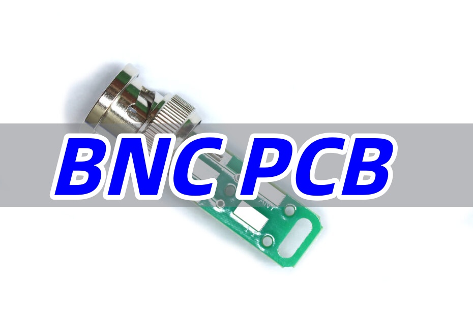
BNC PCB refers to the integration of Bayonet Neill–Concelman connectors directly onto a printed circuit board, providing a robust and reliable interface for coaxial RF connections. This article provides a comprehensive guide on selecting the right BNC connector PCB by examining types, mounting styles, design rules, and performance criteria to ensure optimal signal integrity for your application.
Selecting the right BNC PCB connector is critical, yet many engineers face significant challenges that can derail a project’s performance and timeline.
- Intermittent Signal or Loss: Choosing a connector with an incorrect impedance (e.g., 50-ohm vs. 75-ohm) or poor-quality coaxial interface leads to signal reflections, data corruption, and degraded performance in high-frequency applications.
- Mechanical Failure in Demanding Environments: Standard BNC PCB mount connectors can loosen, break, or detach from the board when subjected to vibration, shock, or frequent mating cycles, causing system failures.
- Incorrect Footprint Leading to Assembly Issues: An inaccurate BNC connector PCB footprint can cause misalignment during SMT assembly, resulting in poor soldering, short circuits, or the need for costly board rework.
- Space Constraints Limiting Design: Finding a suitable connector for ultra-compact devices is difficult; a standard BNC female PCB mount might not fit, forcing undesirable design compromises.
- Poor Performance at High Frequencies: Many standard PCB BNC connectors are not characterized for microwave frequencies, leading to unexpected insertion loss and VSWR (Voltage Standing Wave Ratio) that hamper the performance of sensitive RF systems.
Fortunately, these challenges can be effectively mitigated through informed selection and design practices. The following targeted solutions for reliable BNC PCB integration address these pain points directly.
- Specify Impedance and Frequency Upfront: Always verify if your application requires a 50-ohm or 75-ohm coaxial BNC PCB and select a connector rated for your maximum operating frequency to ensure signal integrity.
- Opt for Robust Mounting Styles: For harsh environments, choose a BNC PCB mount style with robust mechanical features, such as threaded bushings or four-hole flange mounting, to secure the connector firmly to the board and chassis.
- Utilize Certified PCB Footprint Models: Work with suppliers who provide certified, tested BNC connector PCB footprint and layout recommendations, including a BNC female PCB mount vertical 3D model, to prevent DFM (Design for Manufacturability) issues.
- Select Space-Efficient Form Factors: For tight spaces, utilize an ultra-tiny BNC jack PCB or a BNC right angle PCB mount connector to save valuable board real estate and maintain a low profile.
- Choose Connectors with Characterized HF Performance: For RF applications, select BNC PCB connectors that come with S-parameter models (S2P files) to simulate and validate high-frequency performance in your design environment.
As a specialized PCB and assembly manufacturer, BEST Technology provides not only high-quality cable adapters BNC PCB solutions but also expert DFM support. We help you navigate these critical choices to ensure your PCBA projects are built for reliability and performance from the ground up. For a consultation, pls feel free to contact us at sales@bestpcbs.com.
What is a BNC PCB?
A BNC PCB is a circuit board that incorporates a BNC connector, a common type of RF coaxial connector known for its quick-connect bayonet coupling mechanism. This integration allows the board to interface with coaxial cables for transmitting radio frequency signals up to several GHz. They are ubiquitous in applications requiring stable signal transmission, such as test and measurement equipment, video broadcasting, data acquisition systems, and telecommunications infrastructure.
- Function: The primary function is to provide a shielded, impedance-matched transition between a coaxial cable and the traces on the PCB, minimizing signal loss and electromagnetic interference (EMI).
- Importance: A well-chosen PCB BNC is fundamental to maintaining signal integrity, which is the quality of an electrical signal. A poor connector choice can degrade the signal, leading to errors and reduced system performance.
What are the Types of BNC Connector PCB?
BNC connectors for PCBs come in various types, primarily categorized by gender, impedance, and termination style. Choosing the correct type is the first step in the selection process.
- By Gender and Mounting:
- BNC Female PCB Mount: This is the most common type, where the jack is soldered onto the board. It interfaces with a plug (male) on the cable end. Options include BNC female PCB mount vertical and BNC female PCB mount right angle.
- BNC Male PCB Mount: Less common, this connector has the pin and is soldered to the board, mating with a female jack on the cable.
- By Impedance:
- 50-ohm BNC PCB: The standard for most RF and digital data applications. It provides a good balance between power handling and low loss.
- 75-ohm BNC PCB: Primarily used in video signaling (e.g., SDI), audio, and telecommunications where impedance matching to 75-ohm coaxial cable is critical. Using a 50-ohm connector on a 75-ohm line will cause signal reflections.
- By Form Factor:
- Standard PCB Mount BNC Connector: The typical size found on most equipment.
- Mini BNC PCB and Micro BNC PCB: Smaller versions designed for high-density applications where board space is at a premium, such as in compact data acquisition systems.
How Many Ways of BNC Connector PCB Mount can be Used in Your Design?
The mounting style directly impacts the mechanical robustness and assembly of your BNC connector for PCB board. There are three primary ways to mount a BNC connector.
- Through-Hole Mounting: The connector has leads that are inserted into drilled holes on the PCB and soldered. This method offers the strongest mechanical bond, making it ideal for applications subject to high mating force or vibration. However, it requires more board space and is not suitable for high-density designs.
- Surface-Mount (SMT): The connector is soldered to pads on the surface of the PCB. SMT is the standard for automated assembly, allowing for smaller board sizes and higher component density. An ultra-tiny BNC jack PCB is typically SMT. While mechanically weaker than through-hole, proper design with anchoring pads can ensure sufficient strength.
- Press-Fit Mounting: The connector is pressed into a plated-through hole in the PCB, creating a gas-tight connection without solder. This is a highly reliable method used in severe environments with extreme temperature cycling, as it eliminates solder joint fatigue.
What are the Functions of Ultra-tiny BNC Jack PCB in Modern Electronics?
The ultra-tiny BNC jack PCB is a specialized component designed to fulfill critical roles in today’s increasingly miniaturized electronics.
- Space Conservation: Its primary function is to provide a full-featured RF interface in extremely limited space, enabling the design of compact devices like portable oscilloscopes, mini-PCs, and dense server blades.
- High-Density Interconnects: It allows designers to pack multiple RF ports side-by-side on a single board, which is essential for multi-channel systems like data acquisition cards and switch matrices.
- Portable and Handheld Equipment: These connectors are indispensable for battery-operated, handheld test gear and medical devices where every cubic millimeter counts, without sacrificing the performance of a standard BNC interface.
How to Select Coaxial BNC PCB for Your Projects?
Selecting the right coaxial BNC PCB involves evaluating several key parameters against your project’s requirements.
- 1. Frequency Range: Check the datasheet for the maximum frequency rating. Standard BNCs are typically rated for 2-4 GHz, while high-performance versions can reach 10 GHz or more.
- 2. Impedance (50Ω or 75Ω): Match the connector’s impedance to your circuit and cable. Mismatch causes signal reflections, measured as a high VSWR (e.g., VSWR > 1.5:1 is generally undesirable).
- 3. VSWR (Voltage Standing Wave Ratio): This measures how well the impedance is matched. A lower VSWR (closer to 1:1) indicates better performance and less signal reflection.
- 4. Dielectric Withstanding Voltage: This specifies the maximum voltage the connector can withstand between its center conductor and shield, which is crucial for safety and reliability in high-voltage applications.
- 5. Mounting Style and Board Retention: Choose a mounting style (through-hole, SMT) that suits your assembly process and mechanical requirements. For cables that will be frequently connected/disconnected, a connector with a sturdy BNC PCB mount flange is recommended.
What are Considerations for BNC Connector PCB Footprint and Layout?
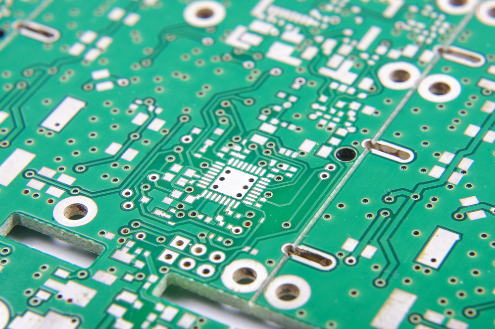
The BNC connector PCB footprint and surrounding layout are arguably the most critical aspects for achieving good signal integrity and reliable manufacturing.
- Footprint Accuracy: Always use the land pattern and drill holes recommended by the manufacturer. An incorrect footprint can lead to poor soldering, tombstoning, or misalignment.
- Impedance Matching to the PCB Trace: The transition from the connector’s coaxial structure to the PCB’s microstrip trace must be impedance-controlled. Use your PCB design tool to calculate the correct trace width for your board’s dielectric constant to maintain the 50-ohm or 75-ohm impedance.
- Grounding and Shielding: Provide an excellent, low-inductance ground connection for the connector’s shield. Use multiple vias around the ground pads to connect the top-layer ground pour directly to the internal ground planes. This creates a continuous return path and minimizes EMI.
- Keep-Out Area: Maintain a clear keep-out area around the connector, as defined in the datasheet, to avoid interference with the board outline or other components.
How to Evaluate PCB BNC for High-Frequency Performance?
Evaluating a PCB BNC connector for high-frequency applications goes beyond just reading the maximum frequency rating.
- Analyze S-Parameters: For critical applications, request or look for S-parameter data (S11, S21) from the supplier. S11 measures the return loss (reflections), and S21 measures the insertion loss (signal attenuation). Good connectors will have low return loss and high insertion loss (low attenuation) across your frequency band of interest.
- Review VSWR Plots: Examine the VSWR vs. Frequency graph in the datasheet. A connector that maintains a low, flat VSWR across the entire frequency range is superior to one where the VSWR rises sharply.
- Time Domain Reflectometry (TDR): A TDR measurement can reveal impedance discontinuities at the connector-to-PCB interface. A smooth impedance profile indicates a well-designed connector.
What Design Rules Improve Reliability of BNC Female PCB in Harsh Environments?
To ensure the reliability of a BNC female PCB connector in harsh environments (vibration, shock, moisture, temperature extremes), follow these design rules:
- Reinforced Mounting: Use a connector with a four-hole metal flange for through-hole mounting. The mechanical strength provided by the four solder points is far superior to a simple SMT pad for withstanding mating force and vibration.
- Strain Relief: Implement strain relief on the cable itself near the connector. This prevents cable weight or tugging from stressing the solder joints on the PCB.
- Conformal Coating: Apply a conformal coating to the entire assembled PCB to protect the solder joints and surrounding circuitry from moisture, dust, and chemicals.
- Material Selection: Choose connectors with robust insulator materials (e.g., PTFE/Teflon) and gold-plated contacts to resist corrosion and maintain stable electrical properties across temperature variations.
Why Choose EBest Circuit (Best Technology) for Cable Adapters BNC PCB and PCBA Projects?
EBest Circuit (Best Technology) stands as your ideal partner for high-frequency and high-reliability BNC connector circuit board projects. Here’s why:
1. 19+ Years of Specialized PCB & PCBA Expertise
- Proven Track Record: Founded in 2006, we possess deep expertise in manufacturing advanced PCBs critical for BNC applications, including:
- High-Frequency Boards: Using Rogers, Taconic, and other specialized materials for optimal signal integrity.
- Metal Core PCBs (MCPCB): Excellent thermal management for high-power adapter designs.
- Heavy Copper PCBs (up to 20 oz): For superior current-carrying capacity.
- Engineering Support: We offer comprehensive support from the start, including PCB design, layout, and DFM (Design for Manufacturability) analysis, ensuring your BNC design is optimized for performance and manufacturability.
2. Comprehensive End-to-End Turnkey Solutions
- One-Stop Service: We simplify your supply chain by managing the entire process under one roof: PCB fabrication, component sourcing, PCB assembly (SMT/THT), and full box-build.
- BNC-Focused Capabilities:
- Impedance Control: Tight tolerances (as low as ±5Ω for values <50Ω) ensure signal integrity in RF applications.
- High-Precision Manufacturing: Fine line/space capabilities (3/3 mil outer layers) and advanced laser micro-vias (0.1mm) for dense BNC layouts.
- Critical Surface Finishes: Options like ENIG, Immersion Silver, and Gold Plating provide excellent solderability and corrosion resistance for reliable BNC connections.
3. Rigorous Quality Assurance and Certifications
- Internationally Recognized Certifications: Our commitment to quality is validated by ISO 9001, ISO 13485, IATF 16949, AS9100D standards, guaranteeing reliability for demanding industries.
- Full-Process Quality Control: Every board undergoes strict inspection at each stage—from incoming materials to final testing—using AOI (Automated Optical Inspection), X-Ray, and Flying Probe Testers to ensure zero defects.
- On-Time Delivery Promise: With a 97% on-time delivery rate and real-time online production tracking, your project timelines are secured.
4. Without MOQ and Rapid Prototyping
- Small Bulk Orders Support without MOQ: We offer transparent pricing for both prototype and mass production runs, with no minimum order quantity (MOQ), providing maximum flexibility.
- Accelerated Lead Times: We understand time-to-market is critical. We offer quick-turn services, with some prototype PCBs shipping within 24 hours, keeping your BNC adapter development on schedule.
5. Customization and Technological Innovation
- Tailored Solutions: We specialize in custom solutions like Rigid-Flex boards for complex adapter housings and high-Tg materials for enhanced thermal reliability.
- State-of-the-Art Equipment: Continuous investment in advanced machinery (e.g., high-precision laser drills, automated SMT lines) ensures we stay at the forefront of PCB technology, ready to meet the evolving needs of connectivity solutions.
Leverage our full-turnkey expertise to streamline your BNC cable adapter PCB projects from BNC connector PCB footprint to SMT assembly. For any specific BNC PCB requirements solutions, please send us an email through the contact form at the bottom of our Contact Page.
In conclusion, BNC PCB integration is a critical design element that directly impacts the performance and reliability of any RF or video system. This guide has detailed the key factors—from types and mounting to layout and high-frequency evaluation—that answer the central question of how to choose the best BNC connector PCB. By carefully considering these aspects, you can avoid common pitfalls and ensure robust signal integrity. BEST Technology possesses the specialized expertise and manufacturing capability to support your most demanding BNC PCB mount and PCBA projects, from prototype to volume production. For expert assistance, please contact us at sales@bestpcbs.com.