GND meaning is foundational in electronics, referring to the ground reference point that ensures stable circuit operation. This article explores the role of GND in circuits, clarifies common misconceptions, and provides practical guidance to avoid grounding errors.
Grounding mistakes can lead to circuit failure, noise interference, or even safety hazards. Whether you’re designing a PCB or troubleshooting a device, understanding GND is critical.
Why do so many engineers struggle with GND circuits?
- Unstable Signals: Noise and voltage fluctuations due to poor grounding.
- PCB Layout Errors: Incorrect GND plane design causing EMI issues.
- Confusion Between GND Types: Mixing analog, digital, and chassis grounds.
- Faulty Reference Points: Incorrect zero-volt reference leading to measurement errors.
- Safety Risks: Inadequate grounding resulting in electric shocks or device damage.
To address these issues, follow these key solutions:
- Implement star grounding to isolate noise-sensitive circuits.
- Use continuous GND planes in PCB design to reduce impedance.
- Clearly separate PGND (power ground) and SGND (signal ground).
- Define a single-point reference for voltage measurements.
- Ensure proper chassis grounding for safety compliance.
At BEST Technology, we specialize in advanced PCB manufacturing, offering robust solutions for complex grounding challenges. Our expertise ensures your designs achieve optimal performance and reliability. Pls feel free to contact us at sales@bestpcbs.com for professional support.
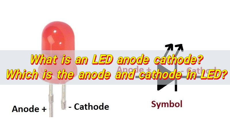
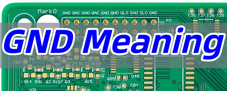
What Does GND Mean?
GND meaning stands for “ground,” the reference point in a circuit where voltage is zero. It serves as a common return path for current and a benchmark for measuring voltages elsewhere in the system.
In electronics, GND is not just a physical connection to the earth—it’s the foundational reference that ensures signal integrity and safety. For example, in a simple battery circuit, the negative terminal often serves as GND. Without a well-defined GND, circuits may suffer from noise, instability, or incorrect logic levels.
What Are the Types of GND Circuits?
GND meaning extends beyond a simple connection—it represents a system of reference potentials that ensure electronic circuits function correctly. Understanding the different types of ground circuits is essential for preventing noise, interference, and operational failures. Below we explore the main grounding schemes used in modern electronics.
1. Digital Ground (DGND)
Digital ground serves as the reference point for digital circuits, which process discrete signals (0s and 1s). These circuits, such as microprocessors and FPGAs, generate high-frequency noise due to rapid switching. DGND provides a stable electrical benchmark, ensuring signal integrity and minimizing cross-talk. In PCB design, a solid DGND plane with low impedance is recommended to handle return currents and suppress electromagnetic interference (EMI).
2. Analog Ground (AGND)
Analog ground is dedicated to analog circuits, which process continuous signals like those from sensors or audio amplifiers. Since analog signals are highly sensitive to noise, AGND must be kept separate from noisy digital return paths. Proper AGND design involves using star grounding or partitioned planes, with a single connection point between AGND and DGND to prevent ground loops and maintain signal purity.
3. Power Ground (PGND)
Power ground handles high currents from power supplies, motor drivers, or converters. Due to large fluctuating currents, PGND can introduce voltage spikes and noise into sensitive circuits. It should be routed using thick traces or dedicated layers, and connected to signal grounds at a single point near the power source. This minimizes interference and avoids ground bounce.
4. Chassis Ground
Chassis ground connects the metal enclosure or frame of a device to the ground system. It serves two key roles:
- Safety: Diverts leakage current away from users.
- EMI Shielding: Acts as a Faraday cage to block external interference.
Chassis ground is typically connected to earth ground in AC-powered systems.
5. Earth Ground
Earth ground involves a physical connection to the ground via a copper rod or grounding electrode. It is primarily used for safety in AC power systems, providing a path for fault currents to dissipate safely into the earth, thereby preventing electric shock.
In summary, effective grounding requires strategic separation and connection of these ground types. For instance, sensitive analog and high-speed digital grounds should remain isolated but linked at a single point to maintain a common reference. Similarly, power grounds must be kept separate to avoid contaminating low-voltage signal paths. By applying the right grounding strategy—such as using split planes, ferrite beads, or star-point connections—you can significantly enhance circuit reliability and performance.
In mixed-signal PCB design, avoid splitting ground planes unnecessarily. Instead, use a unified ground plane with careful partitioning of analog and digital components to reduce return path disruptions.
Why Is GND the Zero-Volt Reference in Electronics?
Voltage is a relative measure; without a reference point, readings are meaningless.
GND provides a stable “zero” level, allowing components to operate with consistent logic thresholds (e.g., 0V for LOW, 5V for HIGH in TTL logic).
For instance, an Arduino’s GND pin ensures all sensors and ICs share the same baseline.
What Are the Differences: PGND vs GND?
While both PGND (Power Ground) and GND (Signal Ground) serve as the zero-voltage reference in a circuit, their roles, design requirements, and applications are fundamentally different. Properly distinguishing between them is critical to avoiding common grounding mistakes that lead to noise, instability, and component failure.
Core Definitions
- GND (Signal Ground): This is the clean reference point for low-power analog and digital signal paths. It is used by sensitive circuits like sensors, microcontrollers, and communication interfaces (e.g., UART, I2C) where signal integrity is paramount.
- PGND (Power Ground): This ground path is dedicated to high-current, often noisy circuits such as motor drivers, switch-mode power supplies (DC-DC converters), and power amplifiers. Its primary function is to provide a low-impedance return path for large, fluctuating currents.
Key Differences Detailed
- Current Handling and Function
- PGND: Handles high currents, from several Amps to hundreds of Amps. Its key role is to minimize voltage drop and power loss in the return path of power circuits.
- GND: Carries only low-level signal return currents (microamps to milliamps). Its purpose is to provide a stable, low-noise reference voltage for accurate signal processing and logic operation.
- PCB Layout and Routing
- PGND: Requires short, wide traces or a dedicated copper pour to reduce parasitic resistance and inductance. It is often directly connected to thermal pads, heatsinks, and the chassis to aid in heat dissipation and safety grounding.
- GND: Focuses on avoiding noise coupling. It is typically implemented as a continuous plane to ensure a uniform potential. Its routing must be carefully planned to stay away from noisy PGND areas and high-power components.
- Noise Considerations and Safety
- PGND: Inherently noisy due to high-speed switching and large current swings (e.g., in a DC-DC converter). It must be isolated to prevent this noise from propagating through the system.
- GND: Must be meticulously protected from the noise and voltage spikes present on the PGND. Its cleanliness is essential for the reliable operation of sensitive components.
The Critical Mistake and the Best Practice Solution
A common and costly error is merging PGND and GND paths on the PCB layout. This allows noisy power return currents to flow through the signal ground areas, creating ground loops and corrupting sensitive measurements.
The best practice solution involves a two-step approach:
- Strategic Separation: Keep PGND and GND physically separate on the PCB layout. This involves defining distinct copper areas for each, preventing the high-current loops of the PGND from overlapping with the sensitive signal paths of the GND.
- Single-Point Connection: Connect the PGND and GND planes at a single point, known as a “star point.” This is typically done near the power input or the main power supply IC. This connection establishes a common system voltage reference without allowing noisy currents to circulate in the signal ground.
For circuits with very high-frequency noise, a ferrite bead can be placed at the star point. This adds high-frequency isolation while maintaining a DC path, further enhancing the cleanliness of the signal ground. By implementing this separation and single-point connection strategy, you directly address a fundamental grounding mistake, leading to a more robust and reliable design.
What Does 10k GND Mean?
- In jewelry, “10k GND” refers to 10k gold (10 karat gold), where “GND” is likely a misspelling or abbreviation.
- In electronics, “10k GND” could describe a resistor (10kΩ) connected to ground, commonly used in pull-down configurations.
How to Define GND in PSpice?
In PSpice, GND must be explicitly defined as node “0” to serve as the simulation reference:
- Place a GND symbol from the
sourceorcapsymlibrary. - Select the component named ”0″ (numeric zero).
- Connect it to the circuit’s return path.
Failing to use the “0” node will result in simulation errors.
What Are the Different GND Definitions in PCB Design?
In PCB design, GND meaning is not a one-size-fits-all concept. It represents a systematic framework for managing current return paths, signal integrity, and safety. The choice of grounding strategy is a cornerstone of robust circuit design, directly influencing noise control, EMI performance, and overall system reliability. Understanding these methodologies is fundamental to avoiding common grounding mistakes.
Core Grounding Strategies
The strategy you choose depends heavily on the operating frequency and the nature of the signals in your circuit.
- Single-Point Grounding: This method connects all ground returns from various subsystems to a single physical point on the PCB, creating a “star” topology. It is highly effective at preventing ground loops, a common source of low-frequency noise.
- Best For: Low-frequency circuits (typically below 1 MHz), sensitive analog systems (e.g., sensors, audio amplifiers), and DC power supplies.
- Drawback: At high frequencies, the long traces to the central point exhibit high impedance, making this approach ineffective and even counterproductive.
- Multi-Point Grounding: In high-speed designs, the goal is to minimize impedance at all costs. This approach connects components to the nearest low-impedance ground plane using the shortest possible path, typically via numerous vias to a dedicated ground layer in a multi-layer PCB.
- Best For: High-frequency digital and RF circuits (above 10 MHz), where providing a minimal-inductance return path is critical for signal integrity.
- Drawback: This can easily create complex ground loops, which are problematic if not managed correctly in mixed-signal systems.
- Hybrid Grounding: Most modern electronics are mixed-signal systems, requiring a blend of strategies. Hybrid grounding uses a single-point connection to tie different ground domains (like Analog GND and Digital GND) together at low frequencies, while each domain utilizes a multi-point plane locally.
- Best For: Systems with ADCs, DACs, or any design combining noisy digital logic with sensitive analog circuits.
- Implementation: A classic example is a “split plane” layout, where analog and digital ground planes are partitioned but connected at a single point under the mixed-signal IC to prevent digital noise from corrupting analog measurements.
- Floating Ground: A floating ground system is not physically connected to the earth (chassis) ground. Its potential is independent, which can effectively break ground loops caused by connections to other equipment.
- Best For: Battery-powered devices, medical isolation equipment, and specific test and measurement scenarios.
- Critical Consideration: Floating systems are susceptible to electrostatic discharge (ESD) and charge accumulation. A standard practice is to connect the floating ground to the chassis through a high-value resistor (e.g., 1 MΩ) to safely bleed off static charge while maintaining DC isolation.
Fundamental Ground Type Classifications
Beyond the overall strategy, it’s crucial to distinguish between the types of ground based on their function:
- Signal Ground (GND): This is the reference point for low-power analog and digital signals. Its primary purpose is to provide a “clean” voltage基准 for accurate signal processing and logic operation. Currents are small, so the focus is on minimizing noise.
- Power Ground (PGND): This path is dedicated to high-current circuits like motor drivers, power supplies, and DC-DC converters. It carries large, fluctuating currents that generate significant noise. The key design goal is low impedance to minimize voltage drops and power loss.
- Chassis Ground: This connects to the metal enclosure of the device, serving two purposes: safety (diverting fault currents) and EMI shielding (acting as a Faraday cage).
- Earth Ground: This is the physical connection to the earth via a grounding rod. It is primarily a safety measure for AC-powered systems.
The core reason for separating, for example, PGND and Signal GND is common impedance interference. Even a small trace resistance can cause significant issues. When a high-power motor’s return current shares the same path as a sensitive sensor’s signal return, the motor’s large current fluctuations will create a variable voltage drop across the trace impedance. This fluctuating voltage effectively injects noise directly into the sensor’s reference point, corrupting the measurement. Proper grounding ensures these return paths do not interfere with one another.
The choice of grounding scheme is a direct response to your circuit’s requirements:
- Low-Frequency, Precision Analog Systems: Prioritize single-point grounding to eliminate ground loops.
- High-Speed Digital Systems: A solid, continuous multi-point ground plane is non-negotiable for signal integrity.
- Mixed-Signal Systems: A hybrid approach with careful layout partitioning is the most reliable method to avoid common grounding mistakes.
A modern best practice for complex mixed-signal PCBs is to use a unified ground plane rather than physically splitting it. The key is to meticulously partition the component placement—grouping all analog components together and all digital components together—over a continuous ground plane. This provides the lowest-impedance return path and avoids the potential antenna effects and complex return paths created by slits in the ground plane.
What Are the Common GND Confusions and Misuse in Circuits?
- Ground Loops: Multiple GND paths causing current circulation and noise.
Fix: Use single-point grounding or isolation transformers. - Floating Grounds: Unconnected GND leads leading to erratic behavior.
Fix: Ensure all GND points are tied to a common reference. - Ignoring Current Return Paths: Narrow GND traces causing voltage drops.
Fix: Use wide traces or dedicated GND planes.
To conclude, GND meaning is the cornerstone of effective circuit design, ensuring stability, safety, and performance. By understanding grounding principles and avoiding common mistakes, you can significantly enhance your electronics projects.
At BEST Technology, we combine precision engineering with practical insights to help you overcome grounding challenges. Pls feel free to reach out to us at sales@bestpcbs.com for PCB solutions that stand the test of quality and reliability.
FAQs About GND Meaning
Q1: Why is Grounding Necessary?
Grounding ensures safety, reduces noise, and maintains signal integrity. Prioritize low-impedance paths, minimize loop areas, and isolate noisy/sensitive grounds. Grounding serves three primary purposes:
- Safety: Protects against electric shock by providing a path for fault currents (e.g., from short circuits) to safely dissipate into the earth.
- Noise Control: Provides a stable reference point (0V) for signals, reducing interference in electronic circuits.
- EMI Mitigation: Minimizes electromagnetic interference by controlling return currents and shielding sensitive components.
Q2: What Are Common Ground Symbols?
- PE/FG: Protective Earth/Frame Ground (safety grounding to chassis or earth).
- PGND: Power Ground (for high-current paths, e.g., power supplies).
- AGND: Analog Ground (for noise-sensitive analog circuits).
- DGND: Digital Ground (for digital circuits with high-frequency noise).
- GND: General signal ground (common reference point).
Q3: Why Does Signal Return Path Matter?
Signals always follow the lowest-impedance path back to their source. Poor return paths cause:
- EMI Radiation: Large current loops act as antennas.
- Signal Integrity Issues: Impedance discontinuities distort signals.
- Solution: Use uninterrupted ground planes under high-speed traces and avoid splitting ground planes across power domains.
Q4: Should Analog and Digital Grounds Be Separated?
Yes. Digital circuits generate high-frequency noise that can corrupt analog signals.
- Separation Method: Use split ground planes for analog and digital sections, connected at a single point near the power supply.
- Exception: If the digital ground is exceptionally “clean” (low noise), they may share a plane.
Q5: How to Ground General Components on a PCB?
- Place components close to a continuous ground plane.
- Minimize vias and trace lengths to reduce impedance.
- Group noisy and sensitive circuits separately.
Q6: How to Ground Interface Connectors (e.g., USB, Ethernet)?
- Use a dedicated “interface ground” isolated from the main signal ground.
- Connect interface ground to main ground via a thin trace or 0Ω resistor to block noise.
- Add filters (e.g., ferrite beads) to interface power/ground lines.
Q7: How to Ground Shielded Cables?
- Connect the cable’s shield to the interface ground (not the main signal ground).
- Ensure the interface ground is clean to prevent noise from radiating via the shield.
- Avoid “pigtail” connections—use 360° clamping for low-impedance bonding.