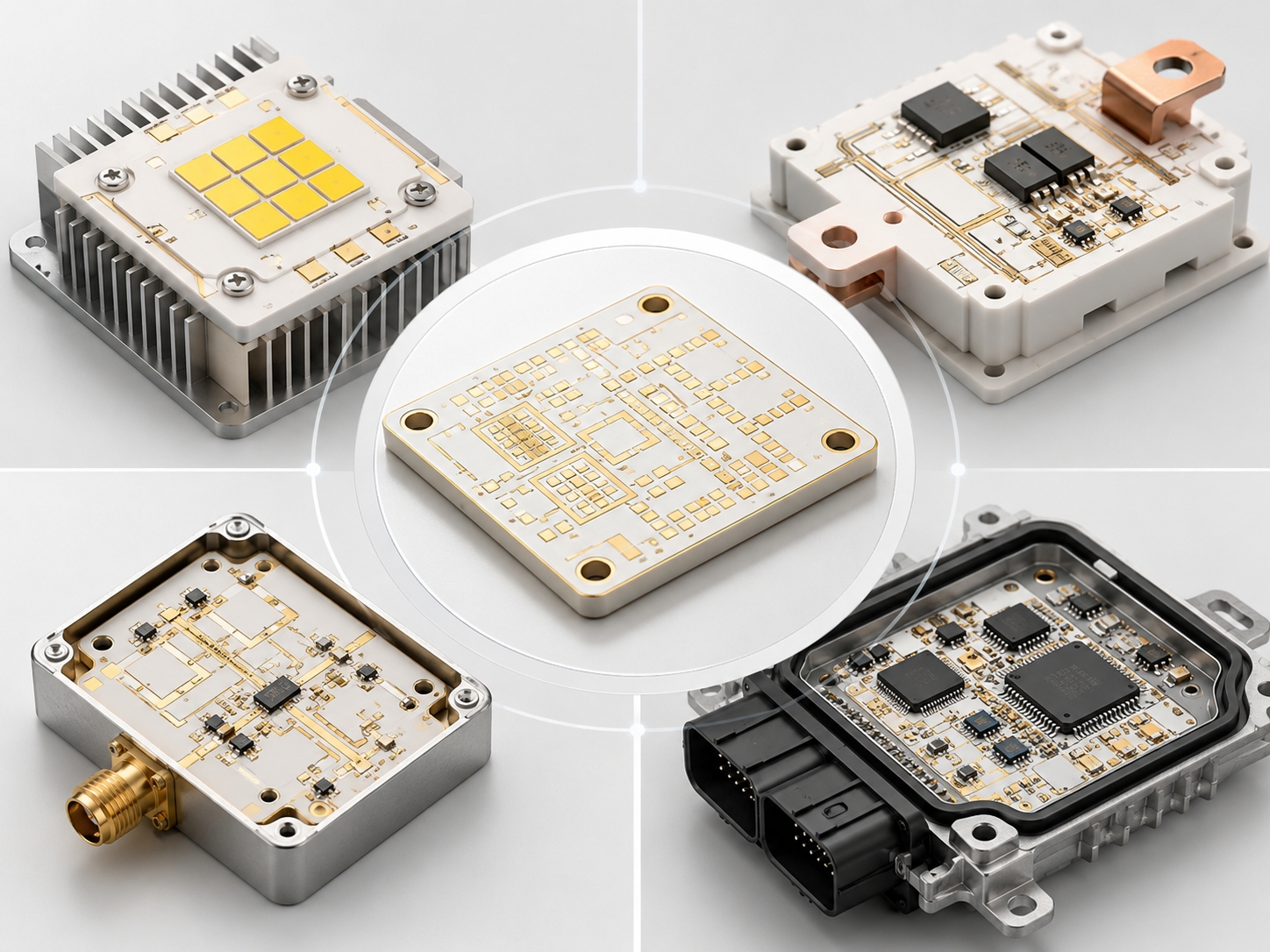
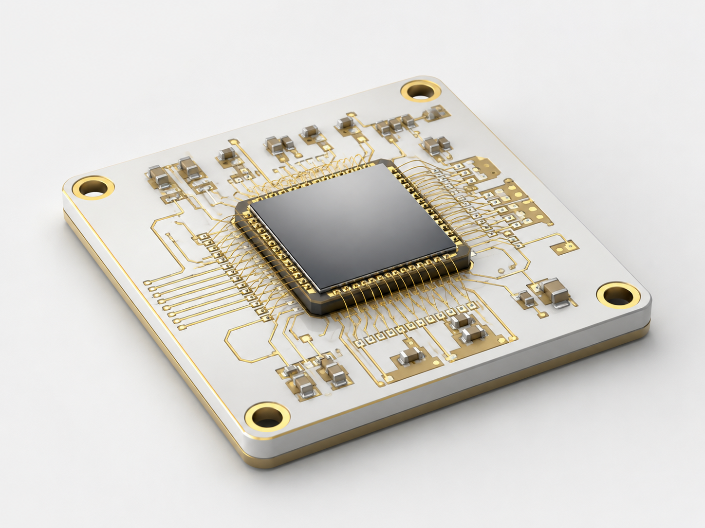
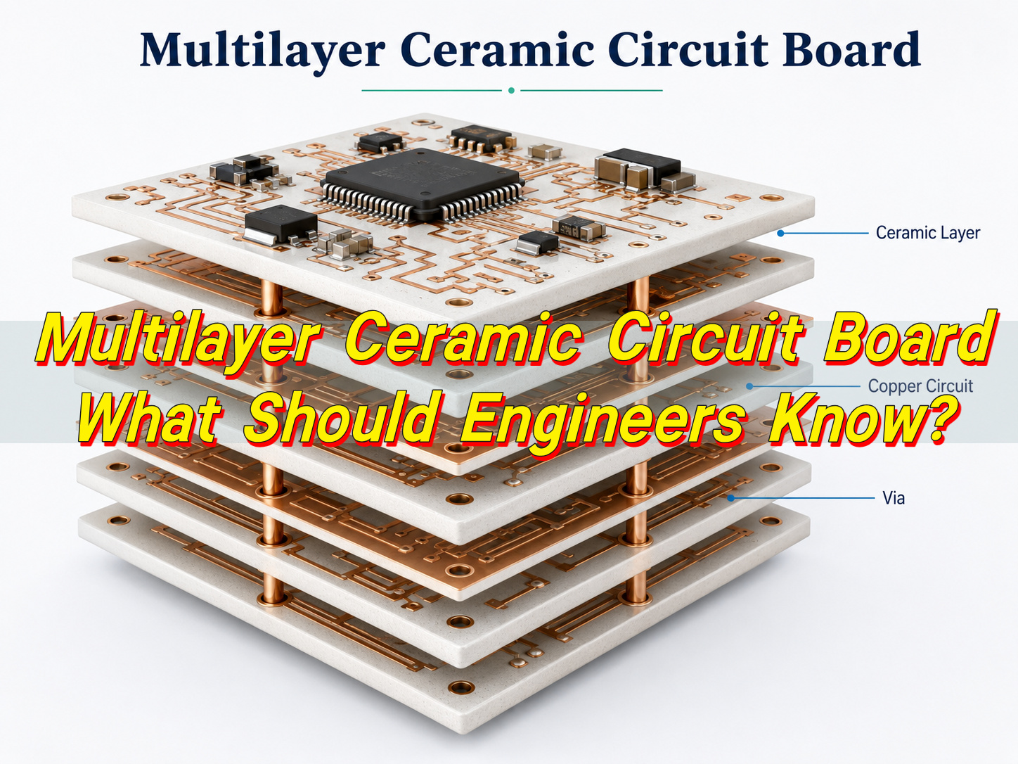
What Is a Rogers Ceramic PCB?
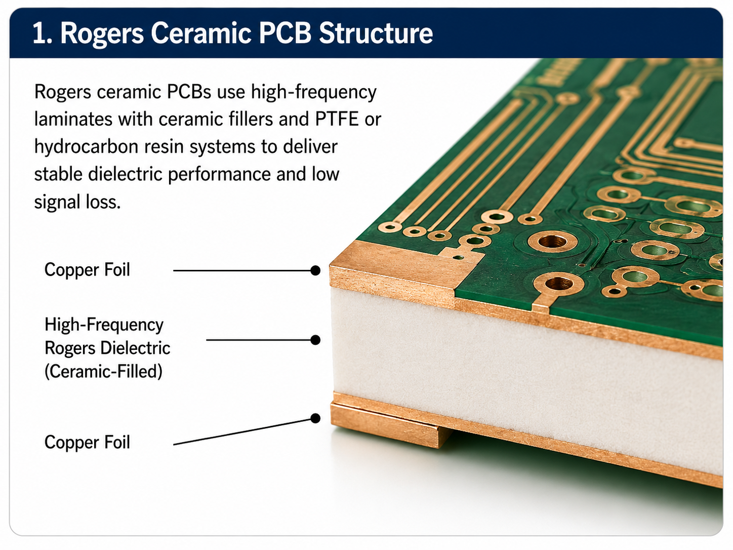
Rogers ceramic PCB usually refers to a printed circuit board made with Rogers high-frequency laminate materials that contain ceramic filler systems. In practical PCB sourcing, this term often describes boards built with materials such as the RO3000 or RO4000 series rather than a fully fired ceramic substrate such as alumina or aluminum nitride.
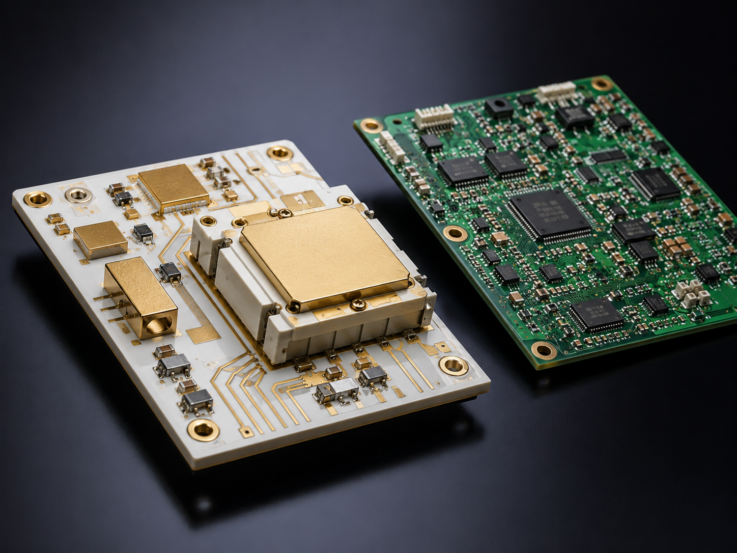
A Rogers ceramic PCB board is designed for circuits where standard FR4 no longer provides enough electrical consistency. When signals move into RF, microwave, millimeter-wave, or high-speed digital ranges, the dielectric material becomes part of the electrical design. The laminate does more than support copper traces. It affects insertion loss, phase stability, impedance control, antenna tuning, and long-term signal behavior. This is why engineers often specify Rogers materials for antenna modules, radar circuits, RF front-end boards, base station hardware, satellite communication circuits, and precision test equipment.
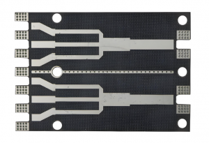
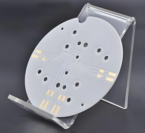
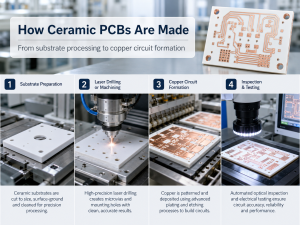
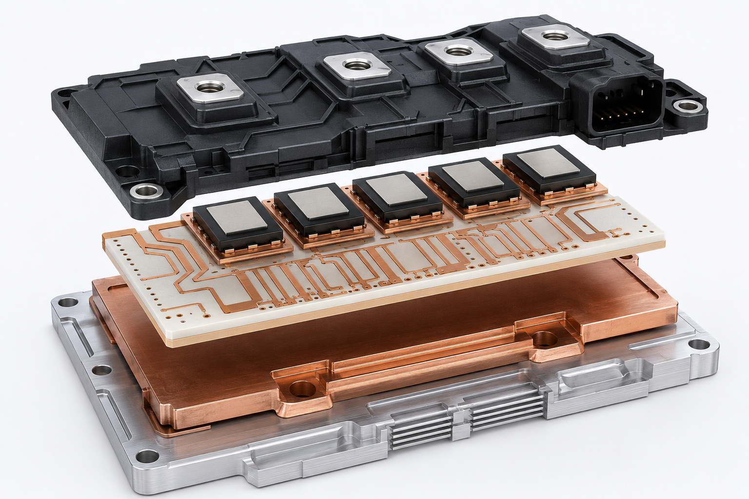
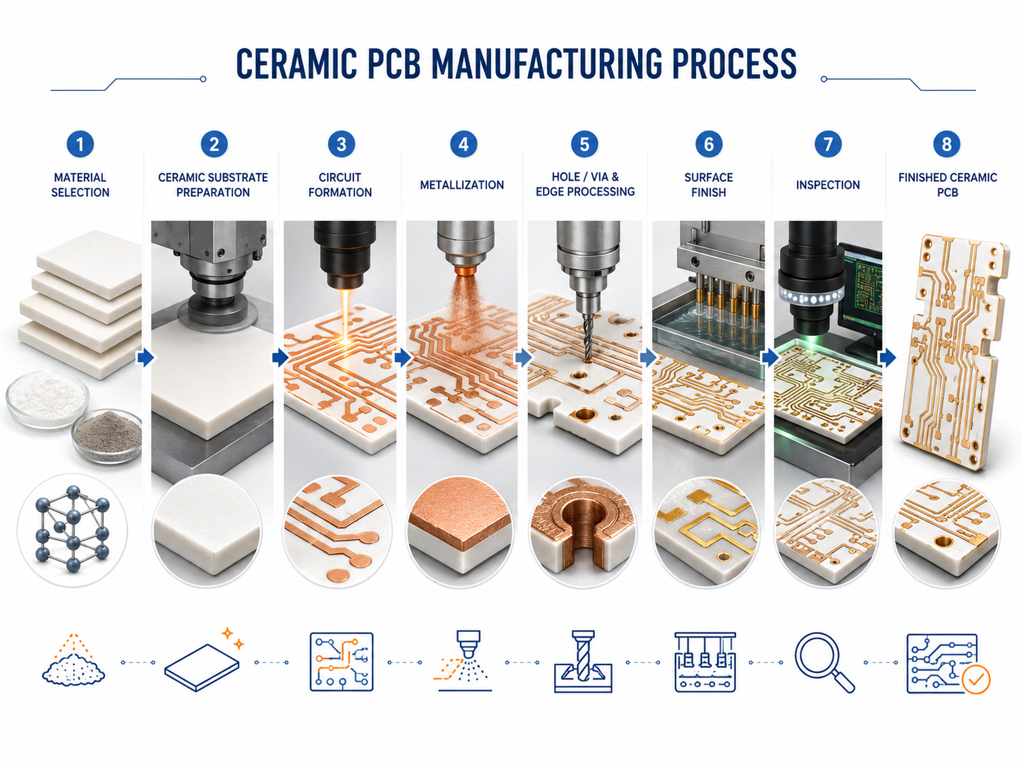
A Rogers ceramic PCB is still manufactured through standard PCB processes such as drilling, copper plating, imaging, etching, lamination, solder mask application, surface finishing, routing, and inspection. The fabrication requirements are more demanding than standard FR4, but the board remains a printed circuit board.
Why Are Rogers Ceramic-Filled Materials Used for RF PCBs?
Rogers ceramic-filled materials are used for RF PCBs because they offer a controlled dielectric platform for signals that are sensitive to loss, phase shift, and impedance deviation. In low-frequency circuits, material variation may have limited impact. In RF circuits, a small change in dielectric constant, copper roughness, trace width, or laminate thickness can shift the electrical result. For antennas, that shift may change resonance. For radar, it may affect range and accuracy. For microwave modules, it may increase insertion loss. For high-speed links, it may influence eye diagram quality.
The ceramic filler helps improve dielectric stability and supports more predictable electrical behavior. In many Rogers material families, the filler system works with PTFE or hydrocarbon resin systems to create a useful combination of low loss, stable Dk, manufacturability, and mechanical reliability.
One of the strongest benefits is lower dielectric loss. Signal loss comes from several sources, including conductor loss, dielectric loss, radiation loss, connector transition loss, and assembly-related discontinuities. PCB material cannot solve every part of the loss budget, but it can make the board more efficient.
Another major advantage is Dk control. The dielectric constant influences the width of controlled-impedance traces, the size of antenna elements, coupling between structures, and the electrical length of transmission lines. When Dk is stable, engineers can design more compact and repeatable RF circuits.
Thermal behavior also supports RF stability. RF modules may experience temperature changes caused by operating power, external environment, soldering, and long service cycles. As temperature changes, the PCB substrate can expand, and its dielectric behavior can shift. Rogers ceramic-filled laminates are designed to reduce these effects compared with many general-purpose materials.
What Rogers Materials Are Commonly Used for Ceramic PCB Boards?
Several Rogers material families can be used for ceramic-filled high-frequency PCB boards. The best choice depends on frequency, loss target, stackup structure, copper profile, thermal requirement, cost target, and assembly process. A China Rogers ceramic PCB manufacturer may offer many of these materials, but buyers should confirm original material availability, laminate thickness options, copper type, lead time, and proven fabrication experience with the selected grade.
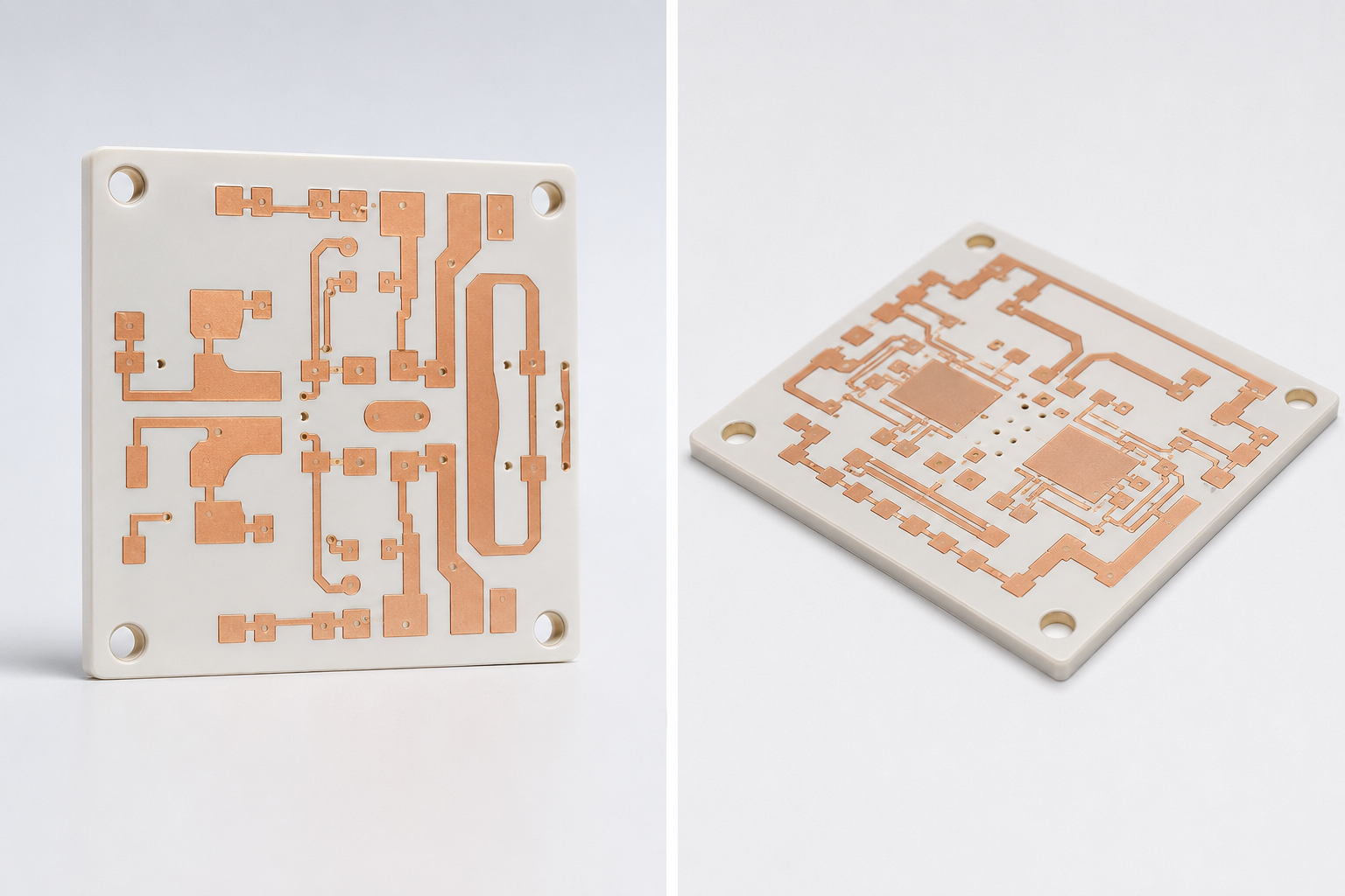
Common material discussions usually include RO3003, RO3006, RO3010, RO3035, RO3003G2, RO4003C, RO4350B, RO4360G2, RO4835, and certain antenna-grade materials in the RO4000 family. These materials are not interchangeable.
Each grade has its own dielectric constant, dissipation factor, thermal behavior, copper options, and processing requirements. A mature Rogers ceramic PCB supplier should help match the material to the circuit instead of recommending only the most familiar laminate.
| Rogers Material | General Material Type | Typical Use Direction | Practical Buying Notes |
|---|---|---|---|
| RO3003 | Ceramic-filled PTFE laminate | RF, microwave, radar, antennas, low-loss circuits | Suitable when low Dk and low loss are important. Often used in radar and mmWave designs. |
| RO3003G2 | Enhanced ceramic-filled PTFE laminate | Automotive radar and mmWave ADAS modules | Designed for next-generation millimeter-wave automotive radar applications. |
| RO3006 | Ceramic-filled PTFE laminate | Compact RF circuits needing higher Dk | Higher Dk can reduce circuit size, but line width and fabrication tolerance require close control. |
| RO3010 | Ceramic-filled PTFE laminate | Miniaturized RF structures, filters, and couplers | High Dk supports compact layouts, but design sensitivity increases as dimensions become smaller. |
| RO3035 | Ceramic-filled PTFE laminate | RF designs needing a mid-range Dk | Useful when the design needs a balance between size, loss, and RF performance. |
| RO4003C | Hydrocarbon ceramic laminate | Cost-sensitive microwave and RF boards | Often selected when designers need RF performance with practical fabrication efficiency. |
| RO4350B | Hydrocarbon ceramic laminate | RF power amplifiers, base stations, and wireless modules | Commonly used in RF circuits requiring stable performance and good production compatibility. |
| RO4360G2 | Hydrocarbon ceramic laminate | Higher-Dk RF circuits and multilayer designs | Useful for compact RF layouts that require higher dielectric constant materials. |
| RO4835 | Hydrocarbon ceramic laminate | RF designs requiring improved oxidation resistance | Suitable for applications where long-term laminate stability is important. |
| RO4500 / RO4700 Series | Antenna-grade laminates | Commercial antenna boards and volume RF designs | Useful for antenna designs where mechanical rigidity and stable installation matter. |
For purchasing, material selection should start from the drawing, stackup, impedance table, and application frequency. A Rogers ceramic PCB factory in China can quote faster when the buyer provides the exact material grade, dielectric thickness, copper weight, finished copper thickness, surface finish, solder mask color, impedance tolerance, hole structure, board outline, and testing standard.
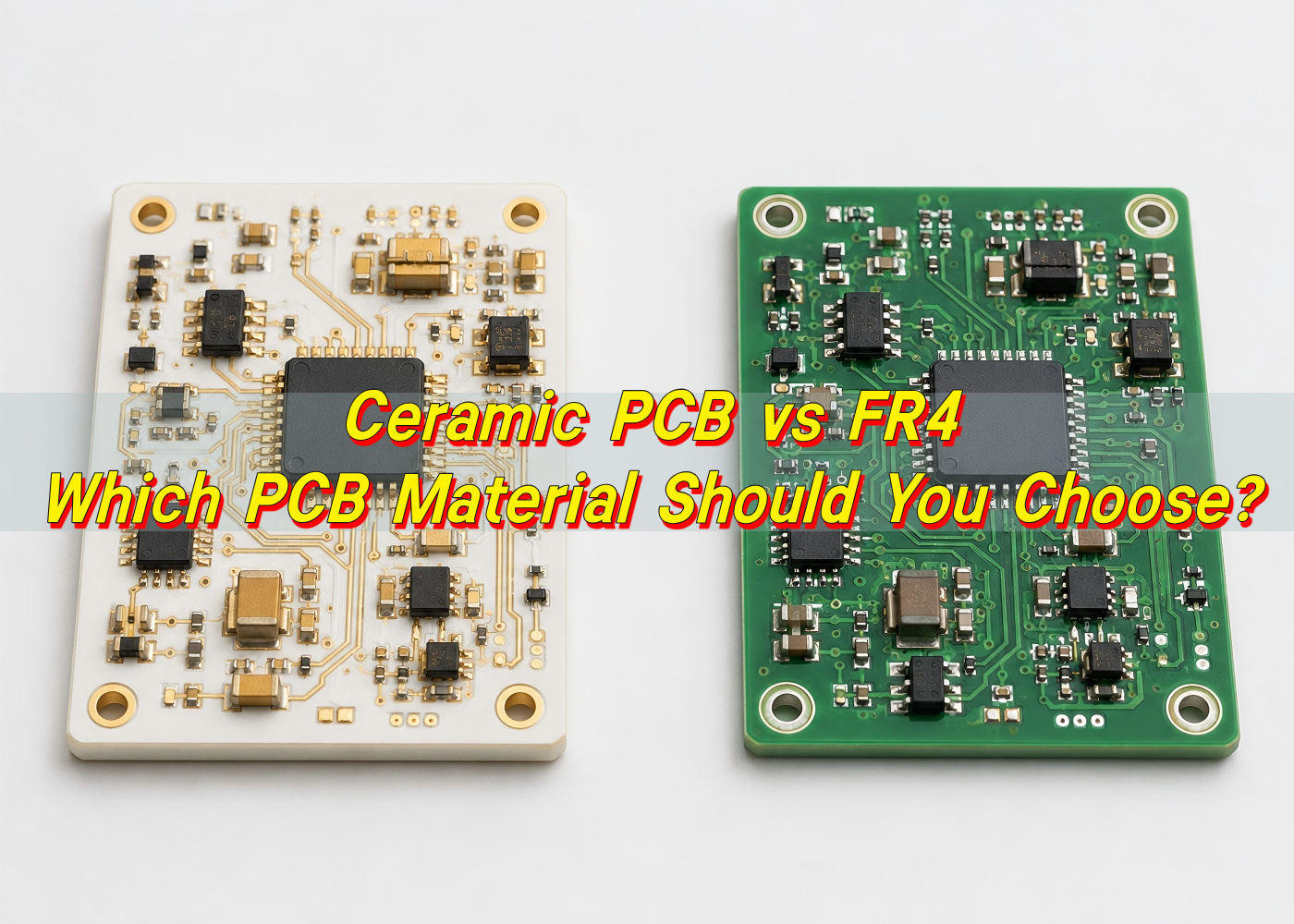
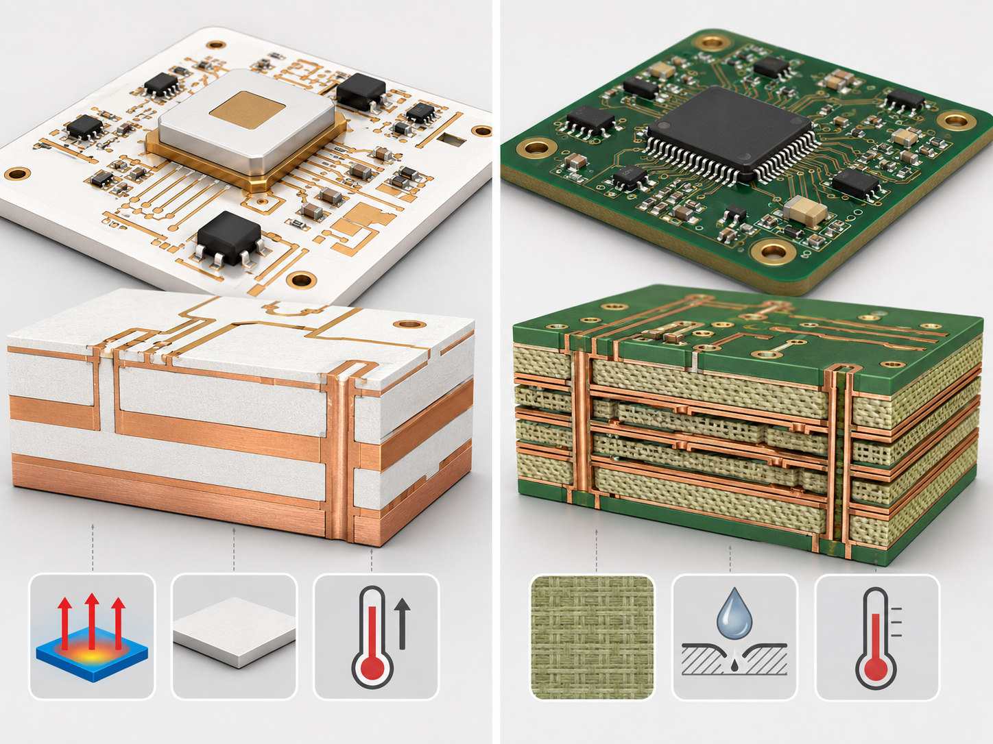
How Is a Rogers Ceramic PCB Board Different from FR4 PCB?
A Rogers ceramic PCB board and an FR4 PCB may look similar after fabrication, but they serve different electrical needs. FR4 is an excellent general-purpose PCB material for many digital, analog, power, control, consumer, and industrial products.
The main difference is dielectric performance. FR4 has dielectric constant and loss characteristics that can vary by resin system, glass weave, frequency, and supplier. Rogers materials provide more controlled Dk and lower-loss options, allowing engineers to design transmission lines and antenna structures with greater confidence.
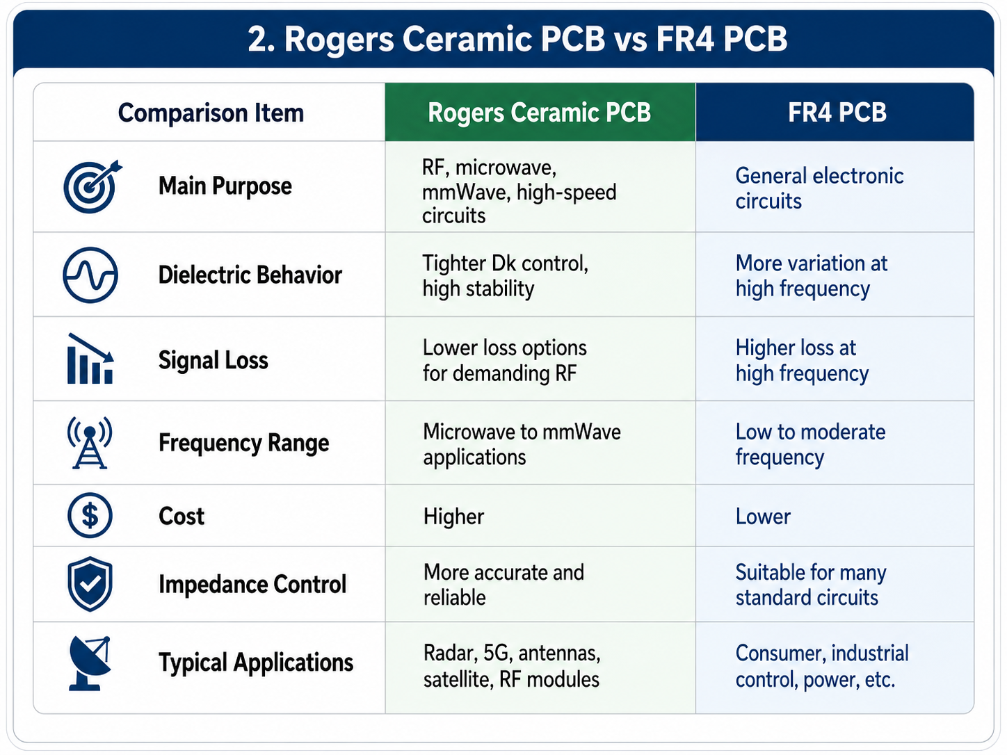
Another difference is frequency suitability. FR4 can support some RF applications at lower frequencies, especially when the design has enough margin and the board structure is simple. As frequency rises, insertion loss and Dk variation become more visible. A high frequency Rogers ceramic PCB is often chosen for circuits where impedance, phase, and insertion loss need closer control. This includes radar boards, RF front-end modules, satellite communication hardware, high-speed test boards, and advanced antenna designs.
| Comparison Item | FR4 PCB | Rogers Ceramic-Filled PCB |
|---|---|---|
| Main purpose | General electronic circuits | RF, microwave, mmWave, high-speed, and controlled-loss circuits |
| Dielectric behavior | Suitable for broad use, with more variation at high frequency | Designed for tighter Dk control and RF stability |
| Signal loss | Suitable for many standard circuits | Lower-loss options for demanding RF paths |
| Frequency range | Suitable for low to moderate frequency applications | Better fit for microwave, radar, antenna, and high-speed applications |
| Cost | Usually lower | Usually higher because of material cost and process control |
| Fabrication difficulty | Familiar and efficient | Requires experienced process control |
| Impedance control | Commonly available | More sensitive and more valuable for RF accuracy |
| Typical applications | Consumer electronics, industrial control, and standard power boards | Radar, 5G, RF modules, antennas, aerospace communication, and test instruments |
| Best buying approach | Standard PCB RFQ may be enough | Provide exact material, stackup, copper, impedance, and inspection requirements |
Hybrid stackups are also common. Some designs use Rogers material only for the RF layers and FR4 for lower-speed control layers. This can reduce cost while preserving RF performance where it matters most. However, hybrid boards need careful lamination planning because material expansion, bonding material, registration, and via reliability must work together. A China Rogers ceramic PCB factory with hybrid stackup experience can help review these details before production.
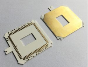
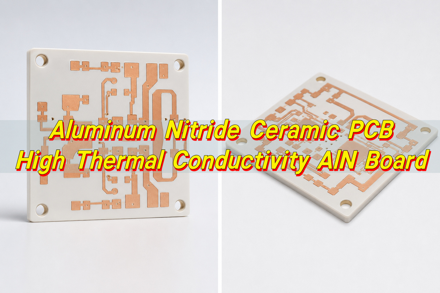
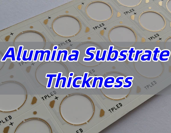
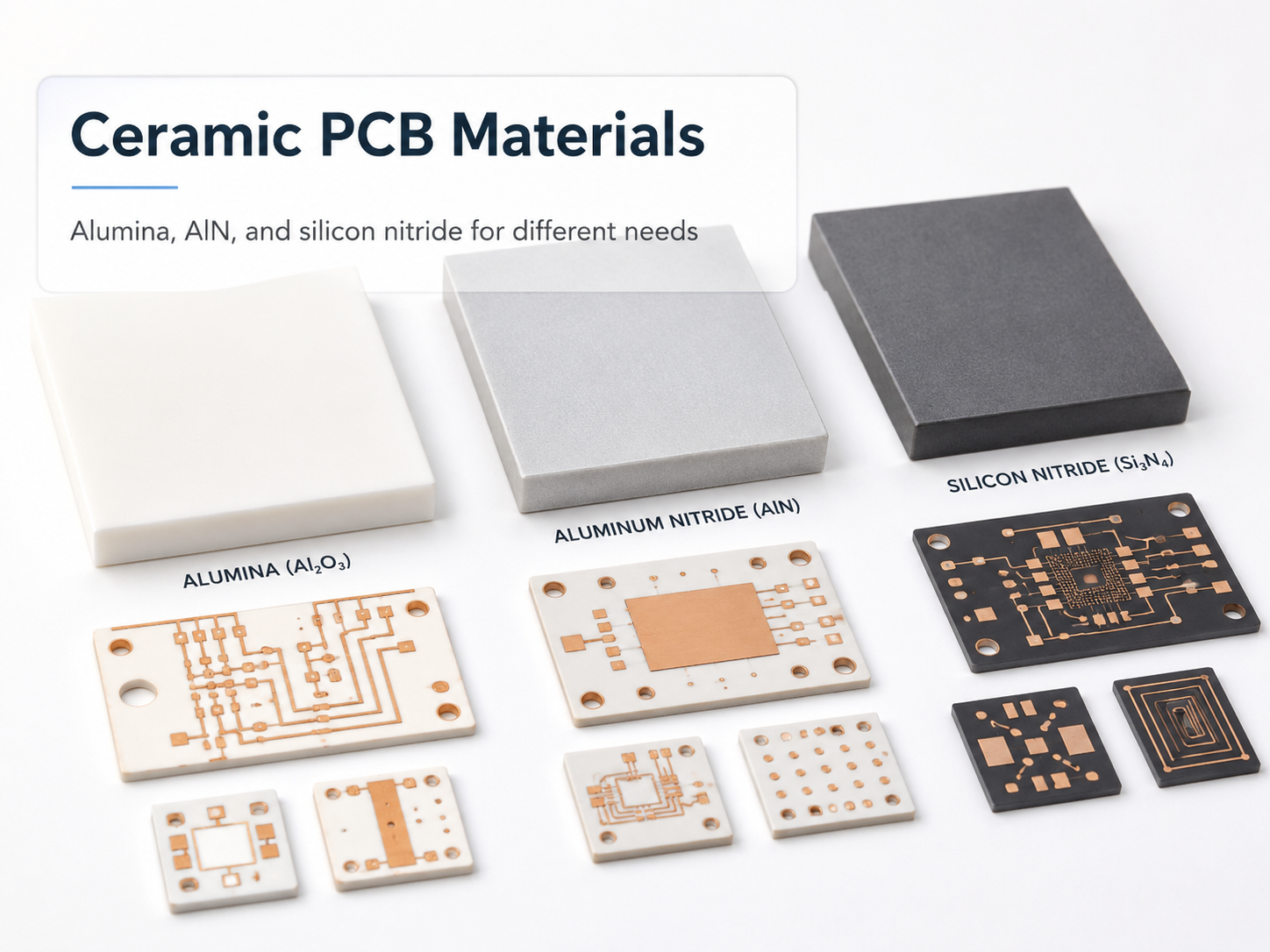
How Is a Rogers Ceramic PCB Different from Alumina or AlN Ceramic PCB?
A Rogers ceramic PCB and an alumina or AlN ceramic PCB are often confused because the word “ceramic” appears in both descriptions. They are different board technologies.
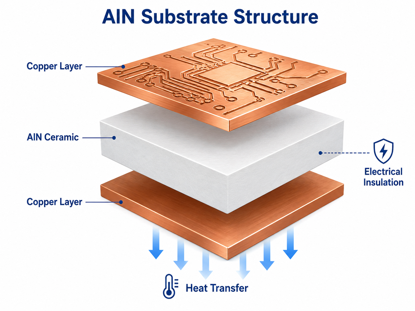
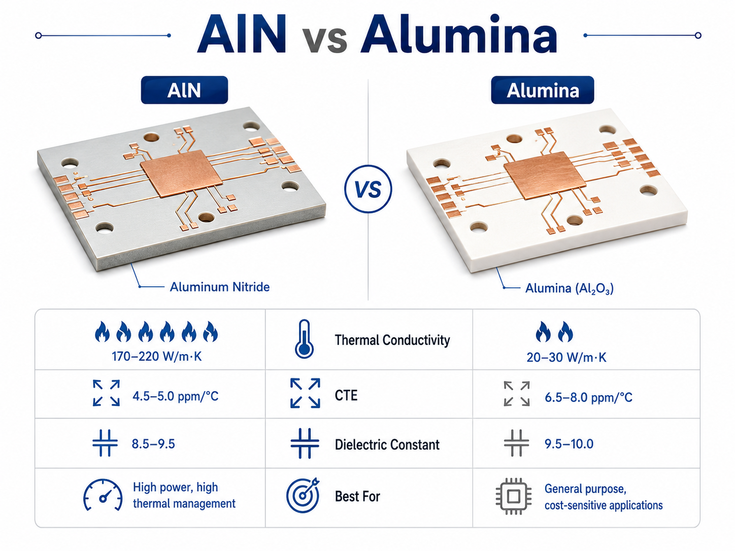
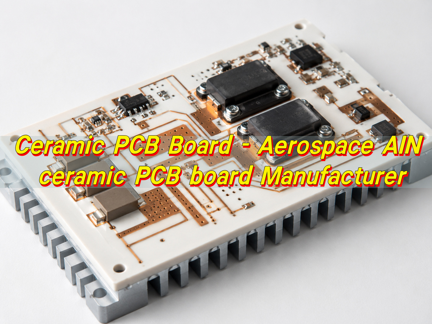
A Rogers ceramic PCB board is usually selected for RF signal performance. It supports low loss, stable dielectric properties, controlled impedance, and PCB-style fabrication. Alumina and AlN ceramic PCBs are often selected for heat dissipation, electrical insulation, high-temperature resistance, power modules, LED substrates, laser modules, and semiconductor packaging. AlN is especially valuable when thermal conductivity is the main design driver.
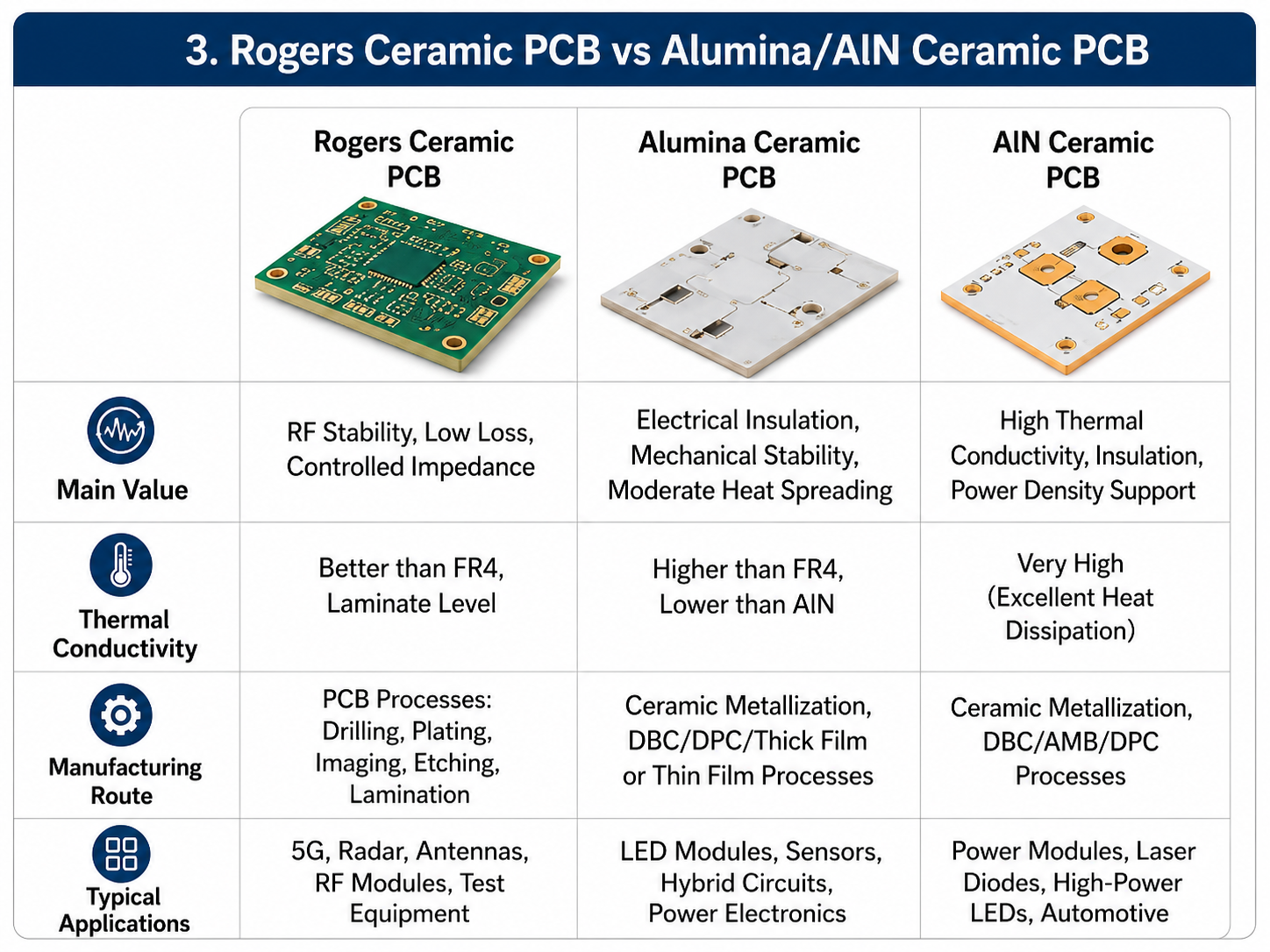
This means the two material categories solve different engineering problems. If the circuit is an RF antenna board, radar module, filter board, or microwave transmission circuit, Rogers ceramic-filled laminate may be the better starting point. If the circuit carries high power density and needs direct heat spreading under chips, MOSFETs, IGBTs, LEDs, or power modules, alumina or AlN ceramic substrates may be more suitable.
| Comparison Item | Rogers Ceramic-Filled PCB | Alumina Ceramic PCB | AlN Ceramic PCB |
|---|---|---|---|
| Material nature | Organic resin system with ceramic filler, such as PTFE or hydrocarbon ceramic laminate | Fired aluminum oxide ceramic substrate | Fired aluminum nitride ceramic substrate |
| Main design value | RF stability, low loss, and controlled impedance | Electrical insulation, mechanical stability, and moderate heat spreading | High thermal conductivity, insulation, and power density support |
| Manufacturing route | PCB drilling, plating, imaging, etching, and lamination | Ceramic metallization, DBC, DPC, thick film, thin film, or related processes | Ceramic metallization, DBC, AMB, DPC, or related processes |
| Thermal conductivity | Better than many standard laminates, but still laminate-level | Higher than FR4, lower than AlN | Very high, often selected for heat-intensive power electronics |
| RF application fit | Strong for RF, microwave, antennas, and radar | Used in some RF packages and circuits, but the design approach differs | Used where thermal control and insulation dominate |
| Mechanical behavior | Similar to advanced PCB laminate handling | Hard and brittle ceramic substrate | Hard and brittle ceramic substrate |
| Assembly format | Familiar SMT and PCB assembly flow | SMT or die attach, depending on metallization | SMT or die attach, depending on metallization |
| Typical applications | 5G antennas, radar boards, RF modules, satellite communication, and test boards | LED modules, sensors, hybrid circuits, and power electronics | Power modules, laser diodes, high-power LEDs, and automotive power electronics |
There is also a supply chain difference. Rogers laminates are specialty PCB materials, but they fit into the PCB supply ecosystem. Alumina and AlN ceramic circuits often involve a different supplier base, different metallization capability, different panel sizes, and different inspection methods.
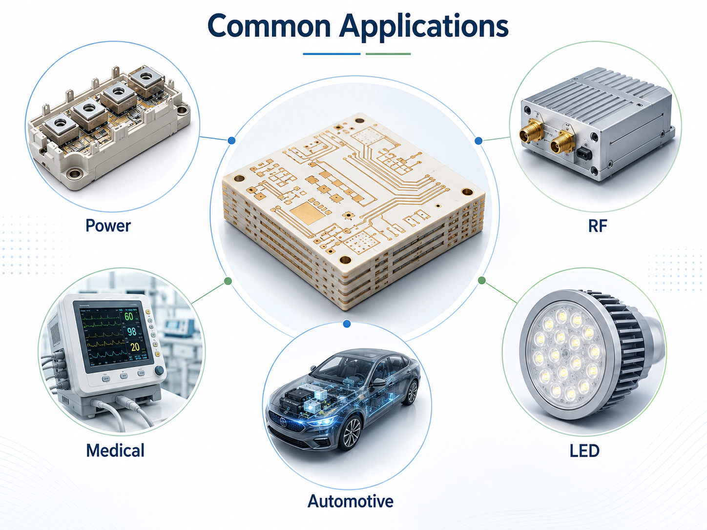
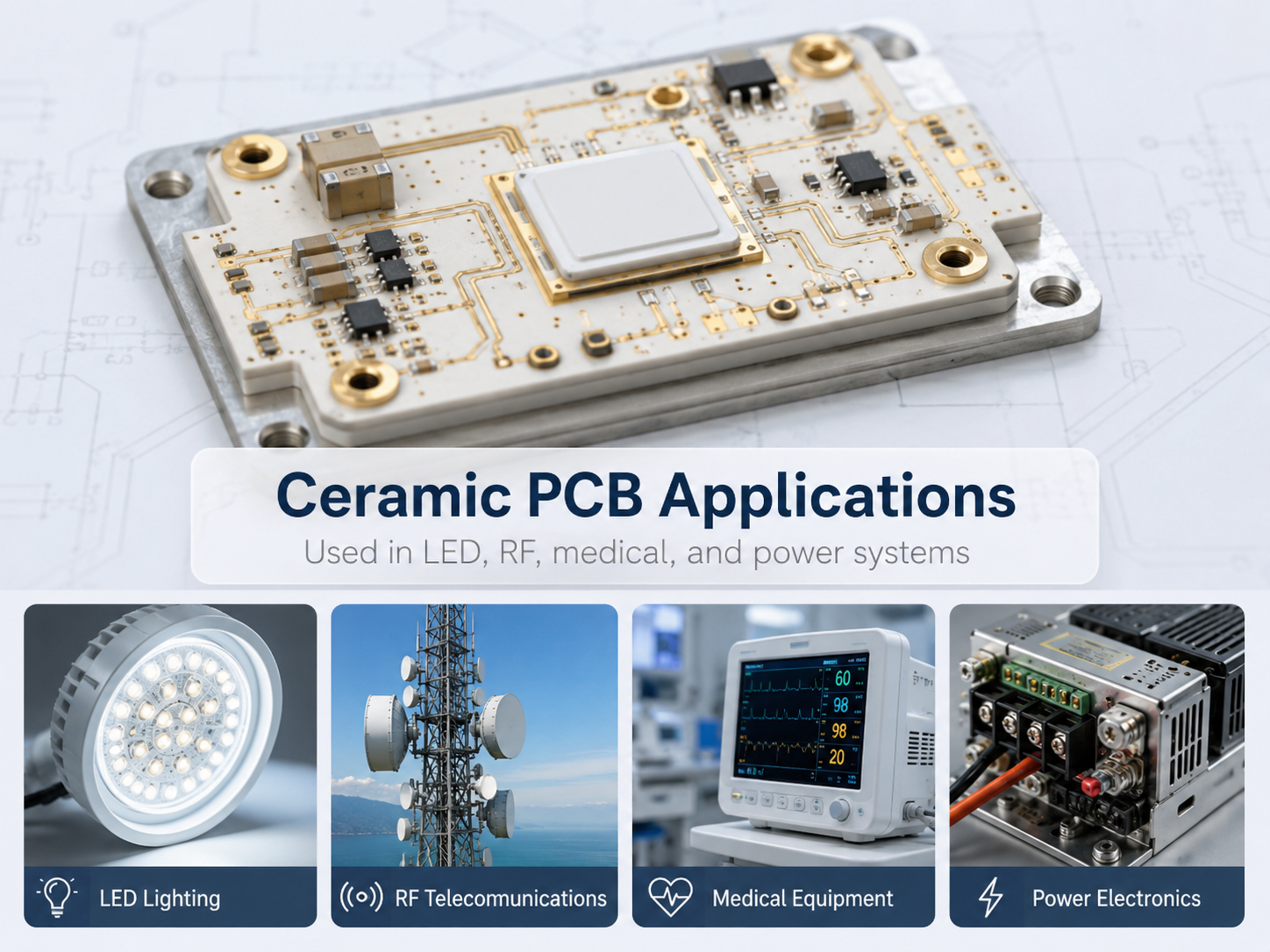
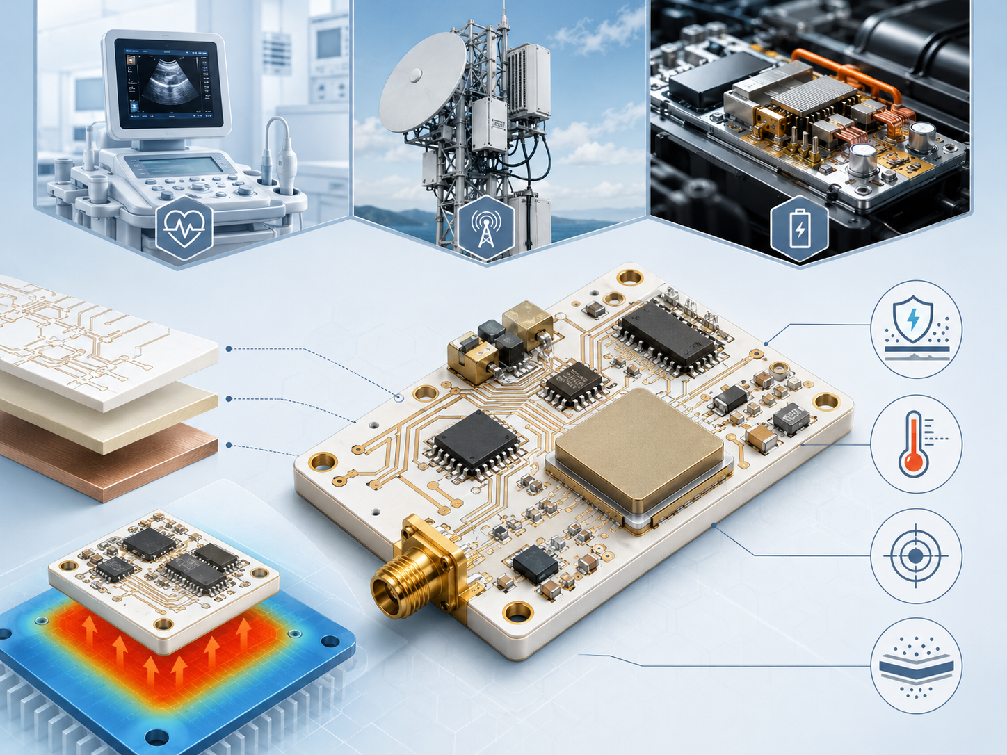
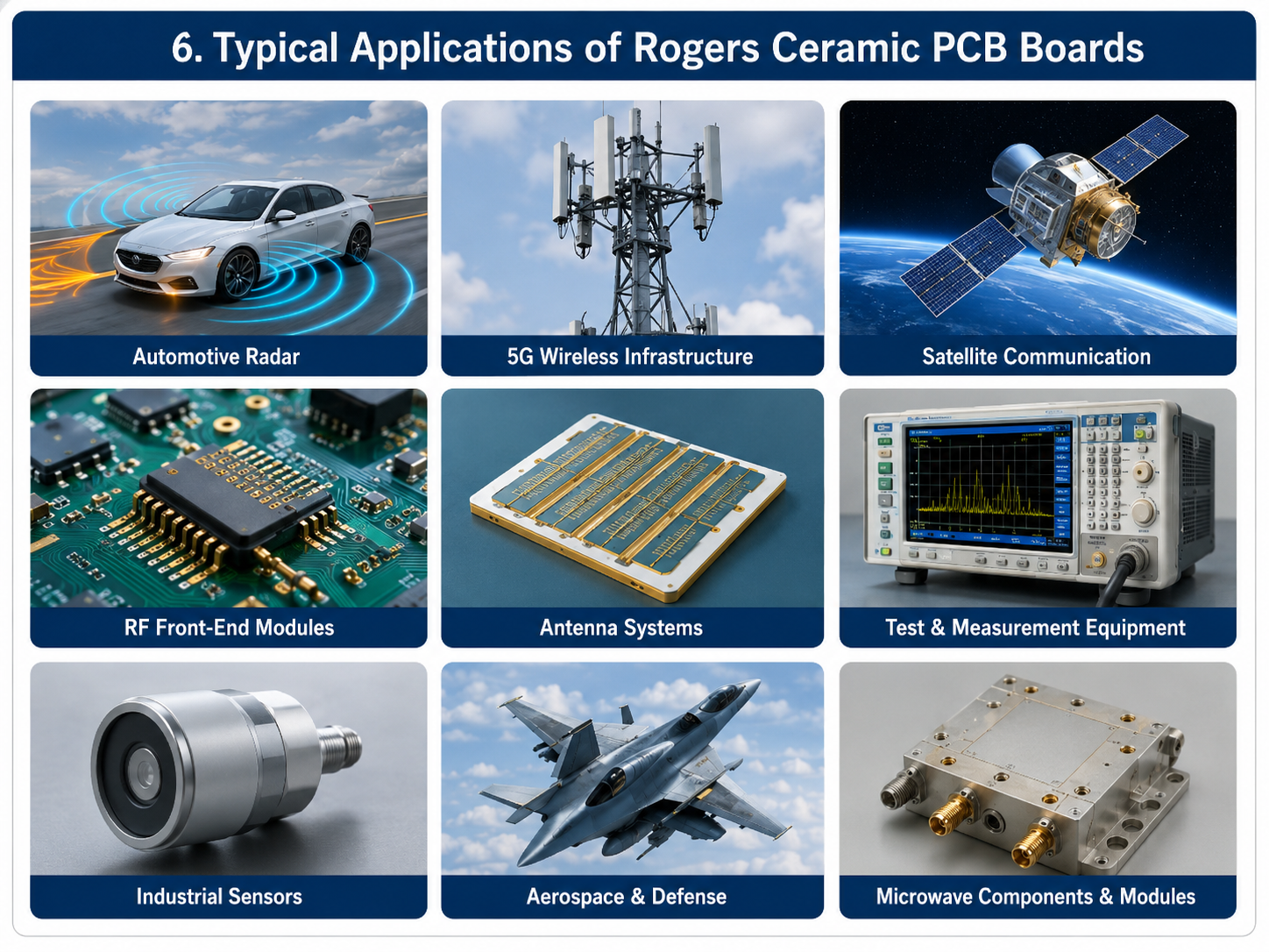
What Applications Use Rogers Ceramic PCB Boards?
Rogers ceramic PCB boards are used where signal quality, RF efficiency, and stable electrical performance carry real product value. These boards are common in communication, sensing, aerospace, defense, automotive, medical, industrial, and test environments.
Typical applications include:
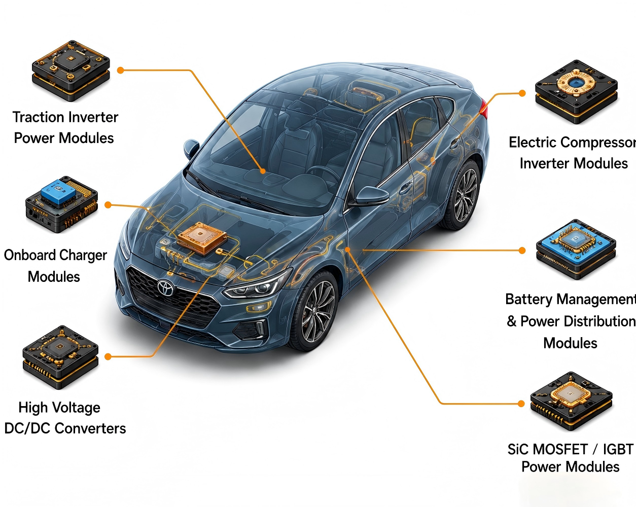
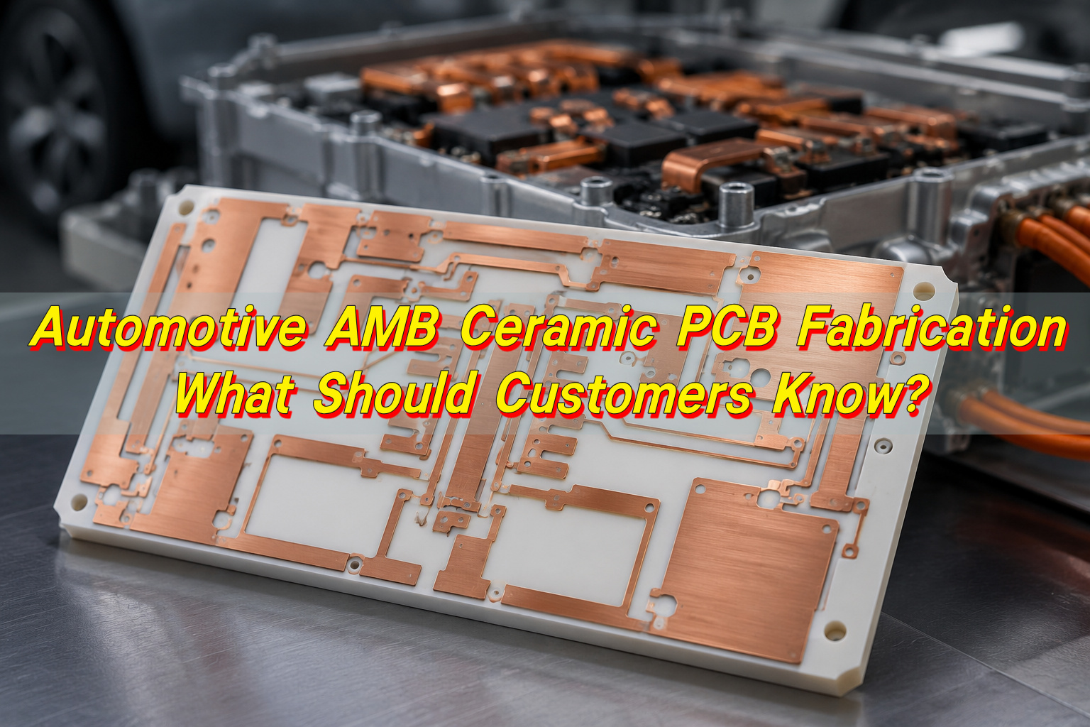
- Automotive radar modules: Rogers ceramic-filled materials are often used in radar and ADAS designs because stable Dk and low insertion loss support accurate radar signal behavior.
- 5G and wireless infrastructure: Base station antennas, RF power amplifier boards, filters, and transceiver modules can benefit from low-loss ceramic-filled laminates.
- Satellite communication and aerospace electronics: Stable phase, low loss, and controlled impedance are valuable in compact RF communication hardware.
- Microwave modules and RF front ends: Mixers, amplifiers, filters, couplers, and low-noise amplifier sections often need predictable laminate behavior.
- Antenna systems: Patch antennas, array antennas, GNSS antennas, and high-frequency communication antennas rely on stable dielectric properties for resonance and gain behavior.
- Test and measurement equipment: High-speed probes, RF evaluation boards, calibration structures, and precision fixtures require repeatable signal paths.
- Industrial radar and sensors: Level sensors, motion sensors, presence detection modules, and mmWave sensing products can use Rogers materials for stable RF performance.
In automotive radar, the PCB is part of the sensing chain. It supports antenna structures, RF transmission paths, and transitions between chips and radiating elements. A small material deviation can influence beam behavior or signal accuracy.
In 5G infrastructure, Rogers ceramic-filled laminates help manage RF loss and signal integrity in high-frequency paths. Power amplifier boards and antenna systems often work under thermal and electrical stress. A material with strong RF stability and manageable fabrication requirements can improve production consistency.
In satellite and aerospace communication, weight, size, reliability, and RF performance need careful balance. A Rogers ceramic PCB supplier in China may support prototypes and production boards for communication modules, but the buyer should confirm documentation, material traceability, impedance reports, microsection reports, and inspection records. In demanding industries, buying only by unit price can create later cost in debugging and qualification.
How Does Rogers Ceramic PCB Support Signal Stability?
A Rogers ceramic PCB supports signal stability by giving the circuit a more predictable dielectric environment. In RF design, the copper trace and dielectric material form a transmission structure. The signal does not simply travel through copper. It travels as an electromagnetic field around the conductor and through the surrounding dielectric. Because of this, the laminate’s Dk, Df, thickness, copper roughness, and temperature behavior all affect the signal path.
Stable Dk supports stable impedance. Controlled impedance is essential for RF transmission lines, high-speed digital links, antennas, and differential pairs. When Dk varies too much, the trace width calculated in the design tool may produce a different impedance in the real board.
Low dissipation factor supports lower dielectric loss. At high frequency, signal energy can be absorbed by the dielectric material. A lower-loss laminate keeps more energy in the signal path, which can improve insertion loss, gain budget, and receiver sensitivity.
Thermal stability also contributes to signal stability. During operation, the board may warm up because of RF power, nearby components, ambient temperature, or enclosure conditions. If the dielectric constant changes greatly with temperature, the circuit can drift.
Copper profile also has a strong effect. At RF frequencies, current tends to flow near the conductor surface because of skin effect. Rougher copper can increase conductor loss and influence phase behavior. Many high-frequency Rogers designs use smoother copper options such as rolled copper, LoPro copper, or very low profile copper, depending on the material and application.
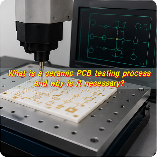
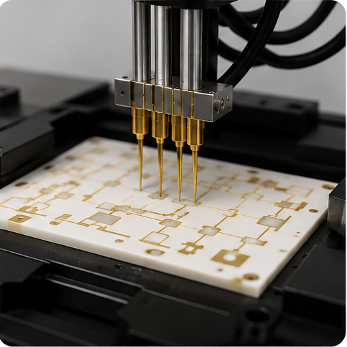
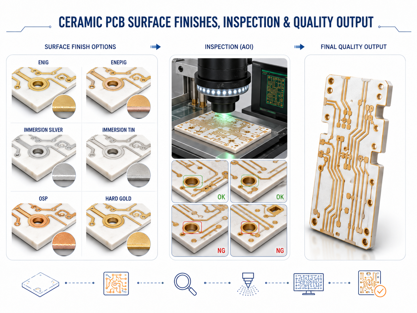
Manufacturing accuracy is equally important. Even the best laminate cannot compensate for poor trace width control, uneven etching, incorrect stackup thickness, unstable lamination, or poorly managed plating. A reliable Rogers ceramic PCB manufacturer in China should control the complete process, including incoming material verification, stackup review, impedance modeling, drilling quality, copper plating, etching compensation, solder mask registration, surface finish selection, AOI, electrical testing, and impedance coupon measurement.
Surface finish can also influence high-frequency performance. ENIG, immersion silver, OSP, and other finishes have different effects on solderability, storage life, wire bonding compatibility, flatness, and RF behavior. For RF pads, antennas, and edge-launch connectors, the finish should be selected with both assembly and signal behavior in mind. The best choice depends on the application, not only on standard factory preference.
A high-quality Rogers ceramic PCB in China can perform very well when the factory understands RF fabrication discipline. The buyer should provide clear impedance requirements, target frequency, stackup drawing, controlled dielectric thickness, copper roughness preference, and inspection requirements.
What Design Factors Affect High Frequency Rogers Ceramic PCB Performance?
High frequency Rogers ceramic PCB performance depends on material selection, stackup design, trace geometry, copper profile, via structure, surface finish, grounding, panel process control, and assembly quality. The laminate is important, but the complete design and manufacturing system determines the final RF result.
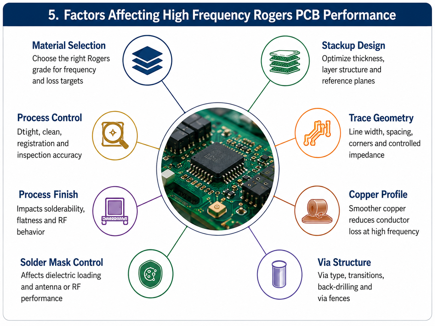
The first factor is material grade. RO3003, RO4350B, RO4003C, RO3003G2, and other Rogers materials serve different design needs. Designers should choose the material based on operating frequency, loss target, Dk value, thickness availability, copper option, cost target, and fabrication route. For example, a 77 GHz radar antenna board may favor very low loss and tight Dk behavior, while a lower-frequency wireless board may use a more cost-balanced RO4000 option.
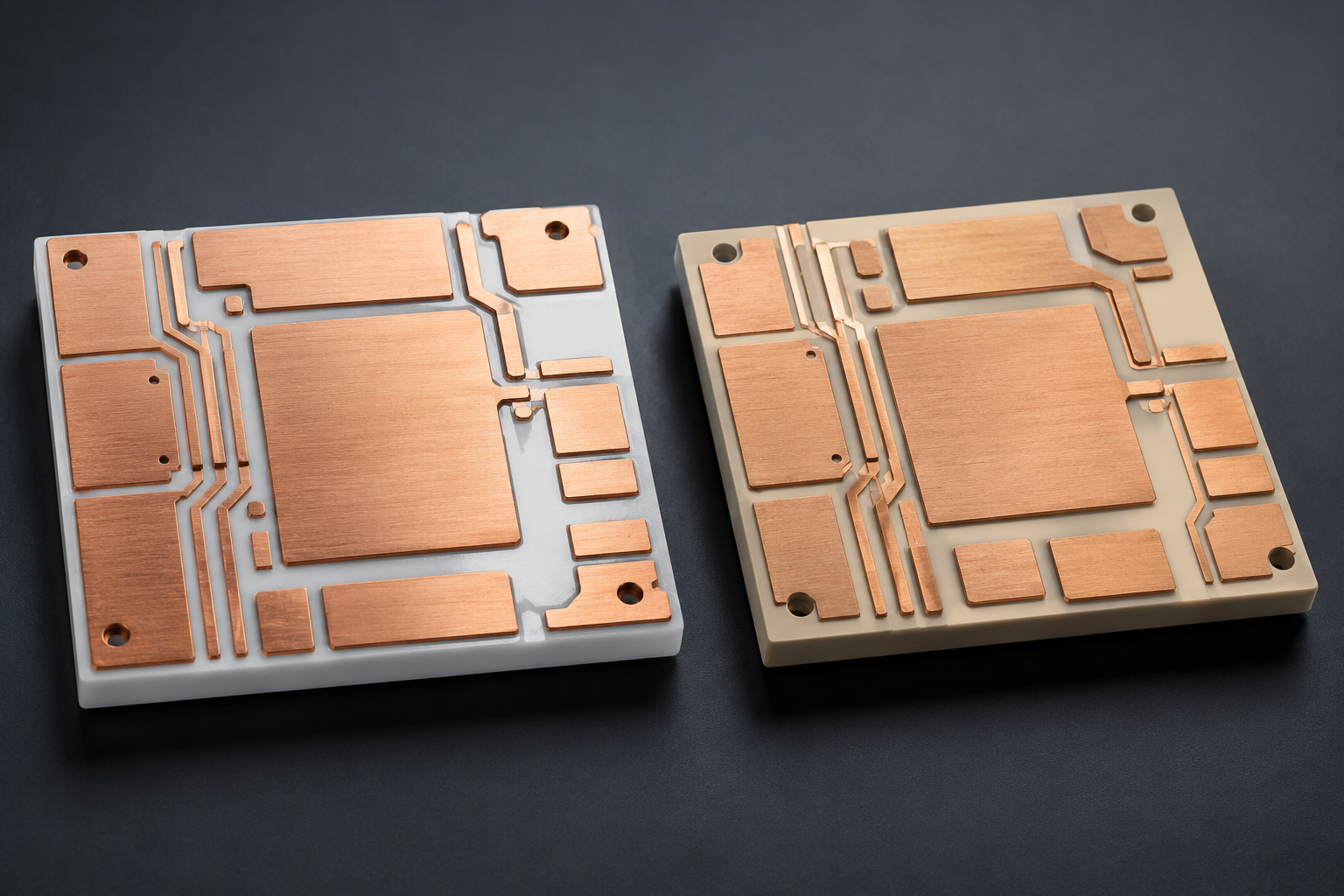
The second factor is stackup. Stackup affects impedance, coupling, crosstalk, shielding, mechanical stability, and assembly flatness. RF layers need controlled dielectric thickness and stable reference planes.
The third factor is trace geometry. At high frequency, trace width, spacing, copper thickness, solder mask opening, corner shape, and launch transition can affect performance. Microstrip, stripline, grounded coplanar waveguide, and differential structures each have their own design rules.
The fourth factor is copper roughness. Smoother copper can help reduce conductor loss at high frequency. However, copper type also affects peel strength, cost, availability, and lamination behavior.
The fifth factor is via design. Vias can create inductance, capacitance, stubs, and mode conversion. RF vias, grounding via fences, back-drilled vias, blind vias, buried vias, and filled vias should be reviewed carefully. In antenna areas, via placement can tune or disturb the radiating structure.
The sixth factor is solder mask control. In many RF areas, solder mask coverage can alter dielectric loading. Some designs keep solder mask away from RF traces or antenna areas. Others allow solder mask in less sensitive areas for protection. The fabrication drawing should clearly define solder mask openings, keep-out zones, and antenna area treatment. This small detail can make a major difference in repeatability.
The seventh factor is panel and process control. Rogers materials may require different drilling, desmear, plasma treatment, lamination, and routing conditions compared with standard FR4. The PCB factory should understand how to protect dimensional stability and hole quality. For high-frequency designs, etching compensation must be precise because trace width directly affects impedance. Inspection should include AOI, electrical testing, impedance testing, microsection when required, and final visual control.
The eighth factor is supplier communication. A buyer looking for a Rogers ceramic PCB supplier in China should send a complete technical package rather than only Gerber files. A clear RFQ package usually includes:
- Gerber or ODB++ data, drill files, IPC netlist, and mechanical drawing.
- Exact Rogers material grade, dielectric thickness, copper weight, copper type, and stackup.
- Controlled-impedance table with target values, tolerance, layer references, and coupon requirements.
- Surface finish, solder mask requirements, RF keep-out areas, and antenna notes.
- Inspection requirements, required reports, quantity, delivery target, and assembly conditions.
In summary, a Rogers ceramic PCB is a high-value choice when RF stability, low loss, impedance control, and repeatable signal behavior matter. Rogers ceramic-filled materials are different from FR4 and also different from alumina or AlN ceramic substrates, so buyers should match the material to the actual engineering requirement. Before buying, confirm the material grade, stackup, copper type, impedance requirements, supplier experience, and inspection records. For Rogers ceramic PCB manufacturing support, material review, or quotation assistance, contact sales@bestpcbs.com