PCB manufacturing PCB manufacturing
Home > Blog

pcb board assembly

PCB Box Build Assembly Services In The USA
Friday, February 27th, 2026

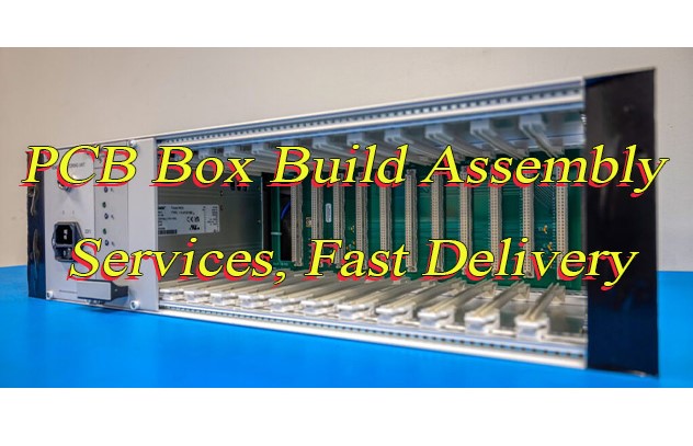
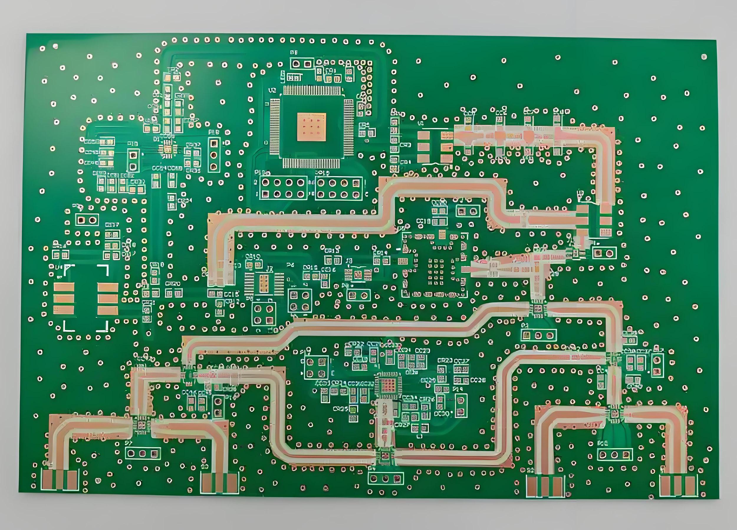
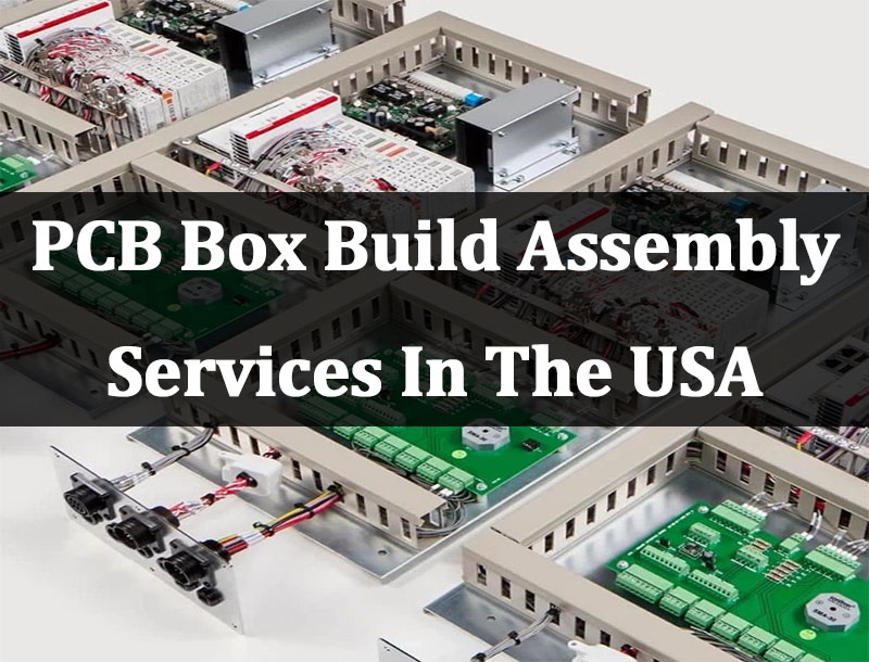
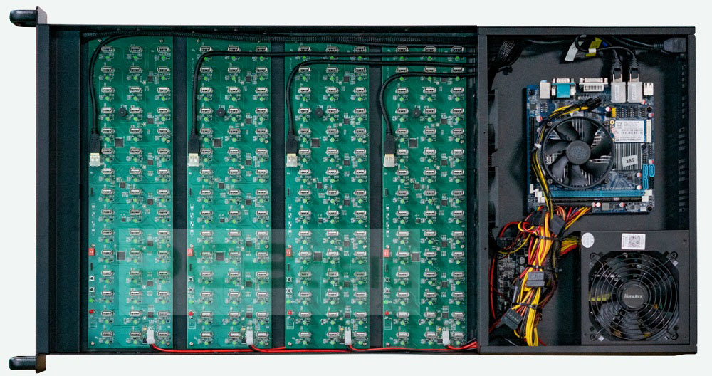
PCB box build assembly services mark the shift from standalone board production to fully integrated system manufacturing. By combining PCB assembly, enclosure integration, cable routing, thermal management, firmware loading, and final validation into one coordinated workflow, they enable U.S. OEMs to achieve stronger reliability, regulatory alignment, and scalable production. This article explains how PCB box build assembly services in the USA operate, how to assess engineering capability, and which design decisions most influence long-term system performance.

EBest Circuit (Best Technology) delivers integrated PCB and box build manufacturing through a vertically coordinated production model that combines PCB fabrication, SMT assembly, cable harness processing, mechanical integration, and system-level testing under one management structure. Serving industrial control, medical electronics, power systems, and high-reliability applications, we support both prototype and volume production without imposing rigid MOQ limitations, ensuring flexibility for U.S. OEMs seeking scalable and engineering-focused manufacturing partnerships. If you have any questions or specific requirements, contact our team at sales@bestpcbs.com.

What Are PCB Box Build Assembly Services And How Do They Extend Beyond PCB Assembly Services?

PCB box build assembly services go far beyond traditional pcb assembly services. While printed circuit board assembly services focus on component placement, soldering, inspection, and functional testing of bare boards, box build encompasses:

  • Mechanical enclosure integration
  • Cable harness and wire routing
  • Power distribution and grounding systems
  • Thermal management implementation
  • Firmware loading and system-level calibration
  • Final assembly, labeling, and packaging

In short, box build transforms individual PCB assemblies into finished, deployable electronic systems.

A typical flow includes:

  1. PCB fabrication and assembly
  2. Subassembly integration
  3. Mechanical enclosure mounting
  4. Cable harness installation
  5. System-level testing and burn-in
  6. Packaging and shipment

This holistic approach reduces handoffs between vendors and minimizes interface-related failures.

How Do Box Build And PCB Assembly Services Support Regulated U.S. Industries?

In the United States, box build solutions are heavily driven by industry compliance and application complexity. Examples include:

Industrial Control Systems

  • Power distribution modules
  • PLC control enclosures
  • HMI interface units
  • High-current bus bar integrations

These systems require strict thermal validation and vibration resistance.

Medical Equipment

  • Patient monitoring devices
  • Diagnostic imaging subsystems
  • Portable therapy equipment

Medical box build requires traceability, documented assembly records, and validation protocols aligned with ISO 13485 environments.

Aerospace And Defense

  • Avionics control units
  • Power conversion modules
  • Ruggedized communication systems

Here, IPC Class 3 workmanship and environmental stress screening (ESS) are typically mandatory.

Box build and PCB assembly services must align mechanical tolerances, grounding schemes, and EMI shielding to maintain certification readiness.

Who Offers Box Build PCB Assembly Services In Illinois With Engineering Depth?

Illinois has a strong manufacturing base, particularly in industrial electronics and medical devices. When evaluating who offers box build PCB assembly services in Illinois, engineers typically assess:

  • In-house PCB fabrication vs subcontracted boards
  • Engineering engagement during DFM review
  • Cable harness design capability
  • UL and IPC certification compliance
  • Lead time stability

A provider with real engineering depth will not only assemble hardware but also:

  • Suggest wire routing optimization
  • Improve airflow within enclosure
  • Recommend connector repositioning
  • Optimize grounding topology

This consultative approach distinguishes strategic partners from simple contract assemblers.

What Defines High-Reliability Box Build PCB Assembly Services In USA?

High reliability is not a marketing phrase. It is measurable.

Key defining characteristics include:

  • IPC-A-610 Class 3 workmanship standards
  • Documented torque control during mechanical fastening
  • Controlled cable bend radius management
  • Ground continuity testing
  • Thermal profiling under load conditions
  • Serialized traceability per unit

In industrial and aerospace programs, providers often conduct:

  • Functional test validation
  • Hi-pot testing
  • Vibration screening
  • Environmental stress screening

These layers ensure that system integration does not introduce latent defects.

Engineering Design Considerations In PCB Box Build Assembly Services

Many reliability failures originate from early design oversights rather than manufacturing errors. Engineers should consider:

Thermal Management

  • Heatsink mounting interface flatness
  • TIM (thermal interface material) selection
  • Airflow channel modeling
  • Fan placement and redundancy

Cable Routing

  • Strain relief anchoring
  • Separation of signal and power lines
  • EMI-sensitive loop reduction

Grounding Strategy

  • Star grounding vs chassis grounding
  • Shield termination placement
  • Earth bond continuity

Mechanical Tolerance Stack-Up

  • Mounting hole alignment
  • Enclosure tolerance allowances
  • Vibration damping materials

Engaging a box build provider during the design stage dramatically reduces redesign cycles later.

From Prototype PCB Assembly To Full Box Build Integration

The transition from prototype pcb assembly to production-level box build often reveals integration gaps.

Common prototype-to-production challenges include:

  • Connector misalignment with enclosure cutouts
  • Cable length miscalculation
  • Insufficient airflow margin
  • Serviceability concerns

Best practice involves:

  • Building pilot runs of 5–20 units
  • Conducting full functional and environmental validation
  • Documenting assembly instructions with photos
  • Locking torque specifications

This structured ramp-up prevents costly mid-production corrections.

Cost Structure Of PCB Box Build Assembly Services In The USA

Cost is influenced by several measurable variables:

  • Labor intensity of mechanical assembly
  • Custom cable harness complexity
  • Testing requirements
  • Enclosure fabrication method
  • Volume scaling

While cheap PCB box build assembly services may appear attractive initially, hidden costs often emerge in the form of:

  • Higher field failure rates
  • Warranty returns
  • Rework cycles
  • Delayed certification

Total cost of ownership should include reliability, lead time predictability, and engineering support—not just unit price.

Case Example: Industrial Power Control Enclosure

A U.S.-based OEM developing a 48V industrial power distribution module required:

  • 6-layer heavy copper PCB
  • Integrated bus bar
  • Forced air cooling
  • Rugged aluminum enclosure

Initial prototype testing showed excessive thermal rise near MOSFET banks.

During box build redesign:

  • Airflow direction was reversed
  • Cable harness was repositioned to reduce airflow obstruction
  • Thermal pad thickness was adjusted
  • Additional chassis grounding was implemented

Result:

  • 18% reduction in peak temperature
  • Improved EMI performance
  • Faster UL validation

This example highlights why box build engineering input is critical early in the product lifecycle.

How To Select A U.S. PCB Box Build Assembly Partner

Engineers should verify:

  • IPC and ISO certifications
  • In-house engineering review capability
  • Supply chain transparency
  • Document control systems
  • Lead time consistency

Questions worth asking include:

  • Is DFM feedback included before mass production?
  • Are torque values documented per unit?
  • Is cable harness manufacturing internal or outsourced?
  • Can they support both PCBA and enclosure integration?

A qualified provider treats system integration as an engineering discipline—not just mechanical assembly.

All in all, as product architectures become more integrated, the distinction between board-level manufacturing and system-level assembly continues to blur. PCB box build assembly services in the USA provide a structured pathway from individual PCB assemblies to fully validated electronic systems ready for deployment in industrial, medical, and aerospace environments.

If you would like assistance evaluating your next project—from printed circuit board assembly services to full system box build integration—our engineering team is ready to review your design files and provide structured feedback. Just feel free to let us know your specific requirements via sales@bestpcbs.com.

FAQs About PCB Box Build Assembly Services

1. What Is The Difference Between PCB Assembly And Box Build?
PCB assembly focuses on populating boards, while box build integrates boards into complete electromechanical systems.

2. Are Box Build Services Only For High Volume Projects?
No. Many providers support low-to-mid volume industrial production.

3. How Long Does A Typical Box Build Project Take?
Lead time varies by complexity, typically ranging from 3 to 6 weeks including validation.

4. Can Box Build Providers Assist With Design Improvement?
Yes, engineering-driven providers contribute to thermal, mechanical, and cable routing optimization.

5. What Certifications Are Important For U.S. Projects?
IPC-A-610, ISO 9001, ISO 13485, and UL compliance are commonly required.

What is pcb board assembly? PCB assembly manufacturer
Thursday, January 2nd, 2025

What is pcb board assembly? PCB board assembly is the process of installing various electronic components (such as resistors, capacitors, chips, etc.) on the PCB and achieving electrical connections through welding and other methods to build a circuit board that can achieve specific electronic functions. This process includes component preparation, PCB board pretreatment, welding and post-assembly inspection.

What is the assembly of a PCB?

What is pcb board assembly? PCB assembly manufacturer

PCB assembly is the process of installing and electrically connecting various electronic components to a printed circuit board according to design requirements. It includes component preparation (purchase inspection, classified storage), PCB preparation (inspection, cleaning), welding (plug-in welding and patch welding) and post-assembly inspection (appearance and electrical performance inspection). Its quality is crucial to the performance and reliability of electronic products and is widely used in consumer electronics, industrial control, communications, automotive electronics and other fields.

How do you assemble a PCB board?

  • Component preparation: Purchase electronic components according to design documents and check whether the component specifications, models and appearance are qualified. After that, the qualified components are classified and stored by type, packaging form, etc.
  • PCB preparation: Check the appearance of the PCB board for scratches, short circuits and other defects, and wipe it with a special cleaner or alcohol to ensure that the surface is free of oil and dust, and that the pads are flat and free of oxidation.
  • Soldering process: Insert the component pins into the corresponding holes of the PCB, use an electric soldering iron to melt the solder to fill the pins and pads to form solder joints, and pay attention to controlling the temperature and time.
  • SMT soldering: Print solder paste on the PCB pads, place the components with a SMT machine, and then heat them according to the temperature curve through a reflow oven to melt the solder paste to form solder joints.
  • Post-assembly inspection: Perform an appearance inspection to check the solder joints and component installation. Then perform an electrical performance test, use professional equipment to check whether the function is normal, and troubleshoot and repair the faults.

What is the function of PCB assembly?

The main functions of PCB assembly include the following aspects:

  • Electrical connection: The copper wire tracks on the PCB board can connect various electronic components (such as resistors, capacitors, and integrated circuits) to form a complete circuit system. This efficient connection method simplifies circuit design and improves circuit reliability.
  • Component support: PCB provides stable support for components. Through welding and other methods, components can be firmly mounted on PCB, which improves the structural integrity and portability of the equipment.
What is pcb board assembly? PCB assembly manufacturer
  • Circuit protection: The insulating material of PCB can effectively isolate electromagnetic interference and protect the circuit from the external environment (such as moisture, dust, etc.), thereby extending the service life of electronic equipment, especially in harsh industrial environments.
  • Heat dissipation function: In high-performance, high-power electronic equipment, the metal layer (such as copper foil) on the PCB can quickly absorb and disperse the heat generated when the circuit is working, preventing components from being damaged by overheating. By optimizing the design, such as increasing the thickness and layout of the copper foil, the heat dissipation efficiency can be further improved.
  • Space optimization and compact structure: The design of the PCB is not only related to the functional realization of the circuit, but also affects the production cost, production efficiency and subsequent maintenance and replacement. Optimizing the use of space makes the internal structure of electronic equipment more compact and beautiful.

What is the standard for PCB assembly?

The standardization of PCB assembly is one of the important measures to ensure product quality and reliability. The following are the main standards for PCB assembly:

  • PCB board size and positioning: The size and positioning of the PCB board should meet the design requirements to ensure accurate alignment and fixation during the assembly process.
  • Component welding quality: The quality of the welding point is the key. The welding point should be smooth, firm, and burr-free to avoid poor welding, cold welding and other undesirable phenomena.
  • Component arrangement and layout: The arrangement and layout of the components should meet the design requirements to ensure the correct spacing and position between the components to avoid mutual interference.
  • Solder point quality: The solder joint should be firm, smooth, and burr-free to ensure the normal operation of the circuit.
  • Appearance quality: The surface of the PCB board should be clean, flat, and scratch-free, and the components should be arranged neatly and beautifully.
  • Electrical performance: Ensure that the electrical performance of the PCB after assembly meets the design requirements.
  • Weather resistance: PCB assembly should have good weather resistance and be able to work stably under different environmental conditions.
  • Reliability: The durability and reliability of the components should be considered during the assembly process to ensure stability in long-term use.

In addition, the specific assembly standards may vary depending on different application scenarios and product types. During the assembly process, relevant standards and requirements should be followed to ensure the quality and stability of the assembly.

What files are needed for PCB assembly?

The following main files are needed in the PCB assembly process:

  • Gerber file: This is the most critical file in PCB production, which contains the geometric information of each layer of the circuit board, such as copper lines, pads, solder mask and silk screen layers. Gerber files are usually generated by CAD software and saved in a standard format.
  • Drill file (.drl or .xin): This file provides the location and size information of all the drill holes on the circuit board, ensuring that the drill holes are accurately aligned with the circuit pattern.
  • Bill of Materials (BOM): The BOM lists all the materials and components that make up the circuit board, including their quantity, specifications and supplier information.
  • Coordinate files: These files provide the coordinate and orientation information of each component on the circuit board, which is essential for the automated assembly process.
  • Assembly drawings: If the PCB needs to be assembled with other electronic components, it is necessary to provide assembly drawings or assembly instructions, which detail how the components are installed on the circuit board.
  • Test requirements: If the manufacturer is required to perform specific tests, such as functional tests or electrical performance tests, it is necessary to provide test requirements or test instructions files.
  • Design Rule Check File (DRC): Used to verify whether the PCB design meets the manufacturing requirements and standards, helping to find and correct potential problems during the design stage.
  • 3D Model (STEP File): Used to generate a 3D model of the circuit board to help simulate and verify during the production process.
  • Structure Drawing (DXF format): Used to make a CAD structure drawing of the circuit board to ensure accuracy during the manufacturing process.

When providing these files, make sure they are up-to-date, accurate, and match the production requirements. It is also very important to maintain communication with the manufacturer to ensure that they have a clear understanding of the design requirements and can produce as expected.

What are the materials used in PCB assembly?

PCB assembly mainly uses the following materials:

1. Electronic components

  • Passive components: including resistors (used to control current and voltage, with a variety of resistance values, powers and packaging forms), capacitors (used to store charge and filter, there are ceramic, electrolytic, tantalum capacitors and other types, with different capacities and withstand voltage values), inductors (used to store magnetic field energy, with winding and stacked inductors, and the unit of inductance is Henry).
What is pcb board assembly? PCB assembly manufacturer
  • Active components: such as integrated circuits (including various functional circuits, with DIP, SOP, BGA and other packaging forms), transistors (used for amplification and switching functions, with BJT and FET and other types, with different parameters).

2. Welding materials

  • Solder wire: The main component is tin-lead or lead-free alloy, with different diameters, lead-containing solder wire has a lower melting point, lead-free solder wire has a higher melting point, and often contains flux inside.
  • Solder paste: used for SMT welding, it is a mixture of solder powder and flux, and its viscosity and metal content affect the quality of printing and welding.
  • Flux: used to remove metal surface oxides and reduce solder surface tension, available in liquid, paste and other forms, and ingredients include organic acids, rosin, etc.

3. PCB substrate materials

  • FR-4: Commonly used epoxy glass fiber cloth laminate, with good insulation, mechanical strength and thermal stability, and different thicknesses.
  • Ceramic substrate: excellent thermal conductivity and high-frequency performance, such as aluminum nitride and alumina ceramic substrates, suitable for high-power and high-frequency devices.
  • Flexible PCB substrate: used for bendable or foldable devices, the material is soft, and polyimide is often used as an insulating layer.

4. Other auxiliary materials

  • Cleaning agent: used to clean impurities on PCB boards, including alcohol and special electronic cleaning agents.
  • Thermal conductive materials: such as thermal grease and thermal conductive tape, used for heat dissipation of high-power components.

How is a PCB board structured?

The basic structure of a PCB board includes multiple layers, each of which has its specific functions and effects.

PCB boards are mainly composed of the following layers:

  • Top Layer: This is the top layer of the PCB board, which is usually filled with electronic components such as resistors, capacitors, and chips. The top layer not only carries these components, but also is responsible for their connection and wiring to ensure that current and signals can be accurately transmitted.
  • Bottom Layer: Located at the bottom of the PCB board, it is mainly responsible for the laying of ground wires and the connection of auxiliary signal lines. The bottom layer provides a solid support for the circuit board to ensure the stability and safety of the circuit.
  • Inner Layer: Located between the top layer and the bottom layer, it is composed of multiple layers of copper foil stacked to form a complex circuit network. The inner layer is used to conduct signals and power supply, reduce signal interference, and ensure the clarity and accuracy of the signal.
  • Solder Mask Layer: This is a special layer, the main function of which is to protect the pads on the circuit board, prevent the solder from splashing into other areas during the soldering process, and ensure the soldering quality and stability of the circuit.

What is the difference between PCB and PCB assembly?

The main difference between PCB and PCBA lies in their status and function.

1. Definition and function

  • PCB: PCB is the cornerstone of electronic devices, providing physical support and electrical connection for electronic components. It consists of a conductive copper layer and an insulating layer, and is usually manufactured by methods such as chemical etching. The PCB itself does not contain any electronic components, but is just an empty circuit board.
What is pcb board assembly? PCB assembly manufacturer
  • PCBA: Printed circuit board assembly refers to the installation of electronic components on the PCB to form a complete circuit. PCBA is functional and can be directly installed in the final product for use.

2. Cost and complexity

  • PCB: Since there are no electronic components, the manufacturing process is relatively simple and the cost is low.
  • PCBA: Due to the need to install and test electronic components, the manufacturing process is more complicated and the cost is higher. PCBA is more complex and more expensive than PCB.

3. Application

  • PCB: Mainly used to manufacture PCBA, as a support and connection frame for electronic components.
  • PCBA: After assembly, PCBA is used in various electronic devices such as computers, smartphones, home appliances, etc.

In summary, PCB board assembly is an interlocking, delicate and complex process. From the careful selection of component preparation, to the pretreatment of PCB boards, and the final strict control, each step should not be underestimated. It organically integrates various electronic components with PCB boards to become PCBA.