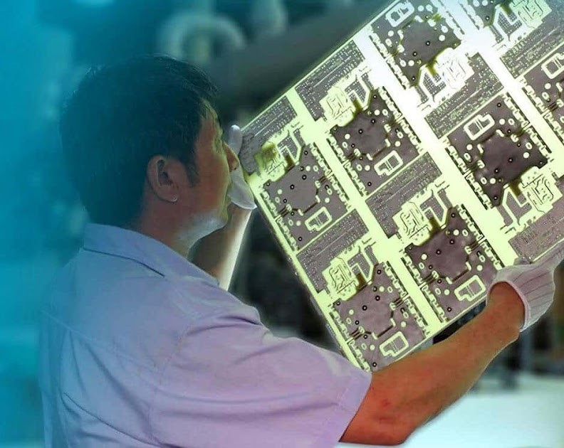
How to assembly a IC board? Let’s discover components, function, application, design spec and guide, assembly process for IC circuit board.
Are you worried about these problems?
- Miss market opportunities due to delivery delays?
- Struggle with high costs squeezing profits?
- Face technical barriers in design realization?
As a IC board manufacturer, EBest Circuit (Best Technology) can provide you service and solutions:
- Reliability assurance: Full-spectrum testing including high-temp/humidity, thermal shock, and vibration extends product life by over 30%, backed by verifiable data.
- Flexible customization: Agile production scales from 50-piece small batches to large-volume manufacturing, with precise BOM traceability to meet diverse needs.
- Eco-compliance guarantee: Full compliance with RoHS 2.0/REACH standards using lead-free solder and recyclable materials, ensuring smooth entry into EU/US markets.
Welcome to contact us if you have any request for IC board: sales@bestpcbs.com.
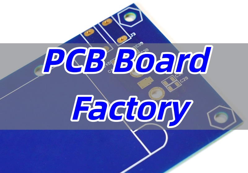
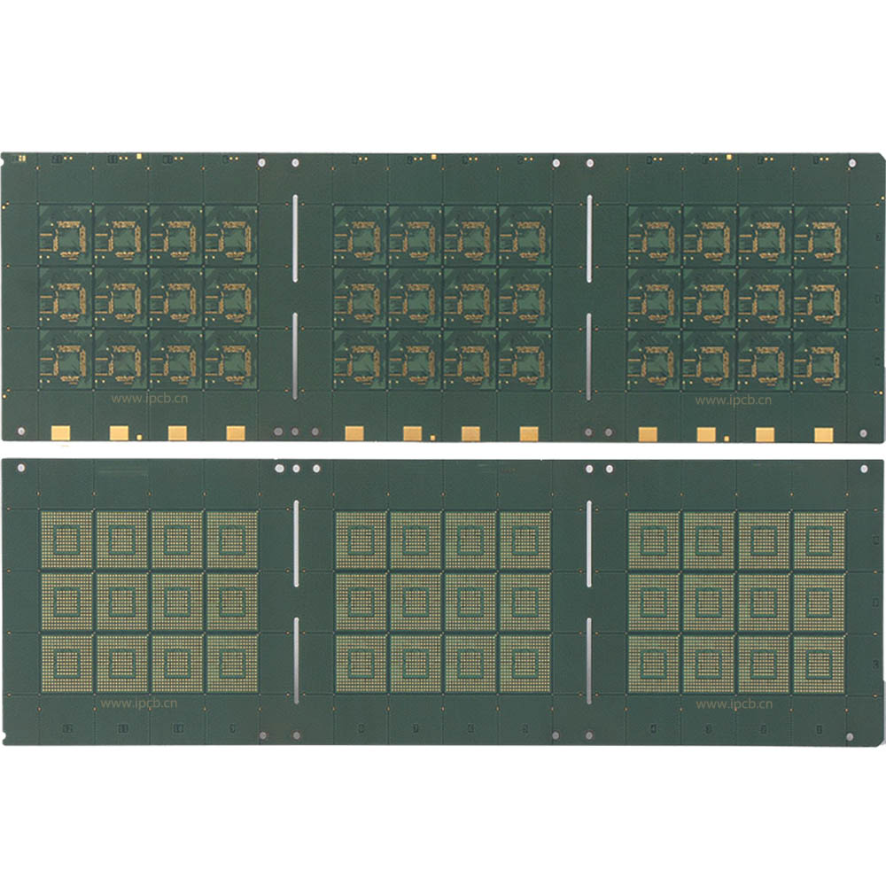
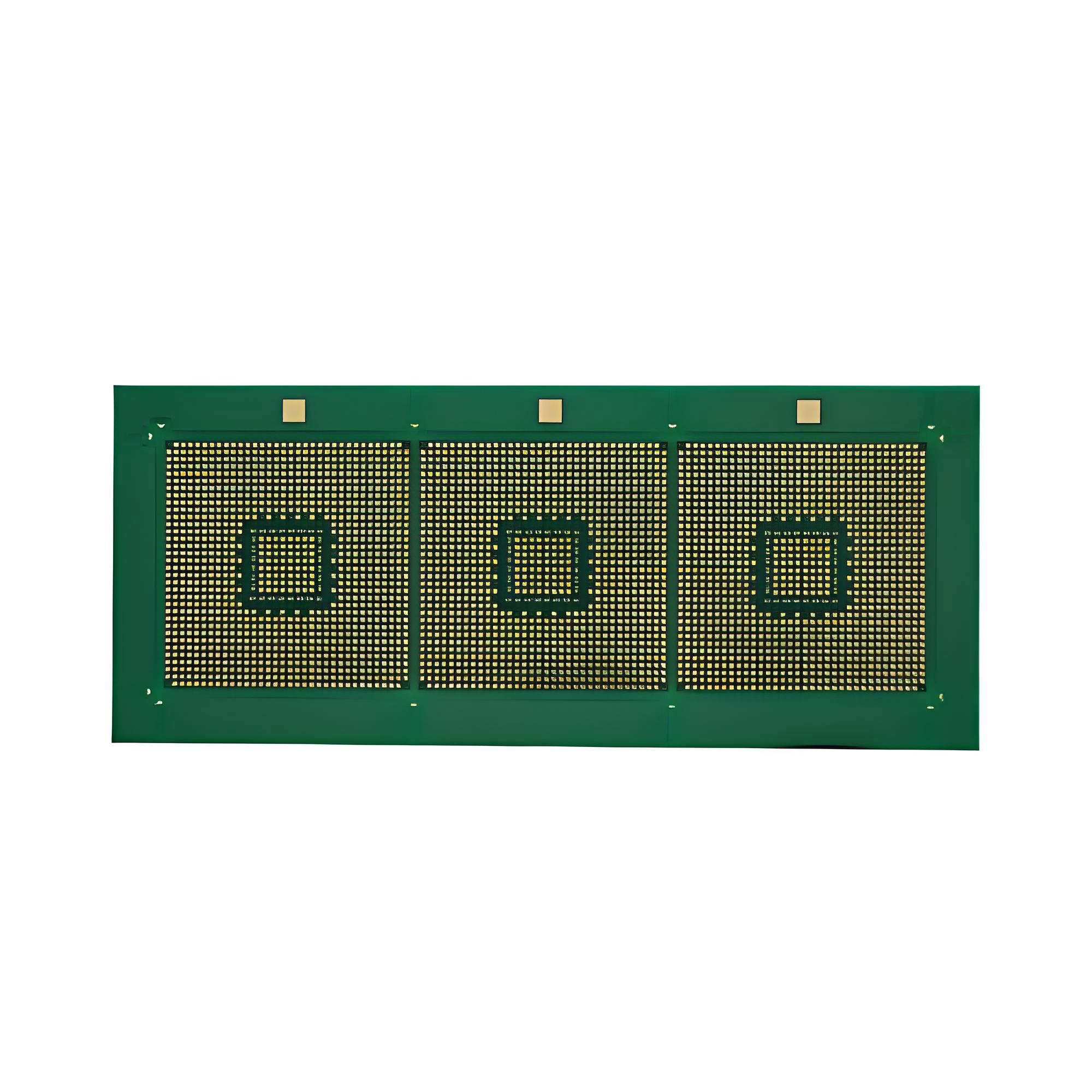
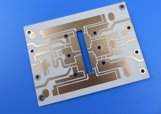
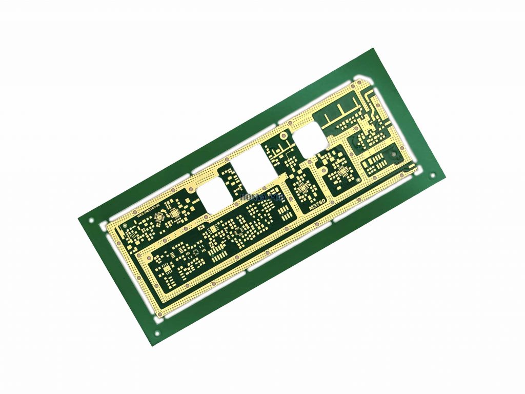
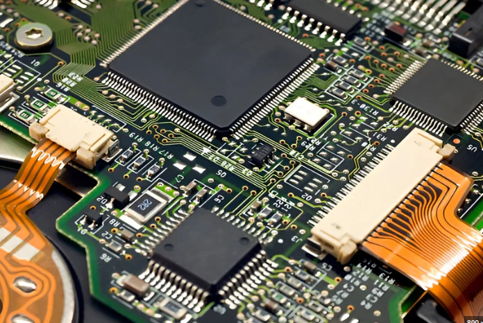
What Is the IC board?
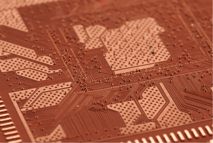
An IC board (also called as Integrated Circuit Board) is a substrate made from insulating materials such as fiberglass epoxy resin, featuring finely etched metal traces (wiring) on its surface. It is used to mount integrated circuit chips (ICs) and other electronic components, providing mechanical support, electrical connection pathways, and forming complete circuits to serve as the core circuit board enabling electronic device operation.
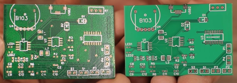
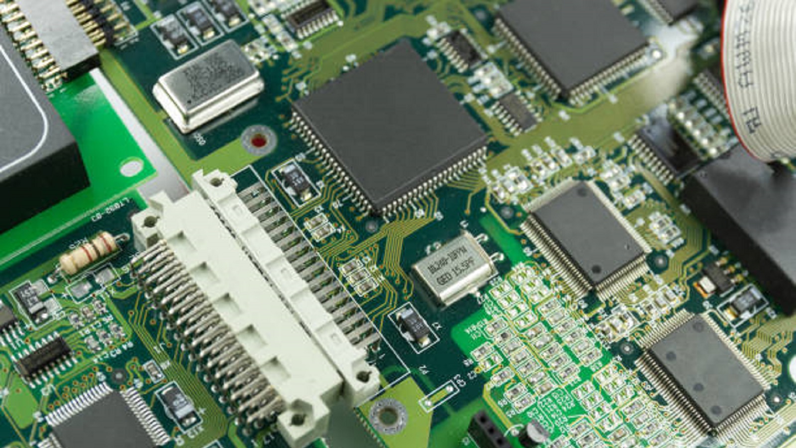
What Are Components of IC Board?
Components of IC Board:
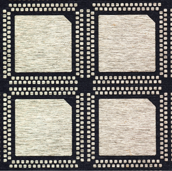
- Substrate Material: The core carrier, commonly made of fiberglass epoxy resin (FR-4), BT resin, ABF film, ceramic substrate (alumina/aluminum nitride), or silicon wafer, providing mechanical support, insulation, and thermal dissipation pathways.
- Metal Wiring Layer: Precisely etched copper or aluminum traces forming a multi-layer electrical network (e.g., power planes, ground planes) with interlayer connections via vias (conductive/non-conductive), enabling signal transmission.
- Component Mounting Areas: Pads, sockets, and surface-mount points for securing chips, resistors, capacitors, and other components while ensuring reliable electrical contact.
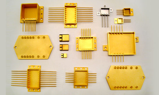
- Packaging Structure: Standard formats such as DIP, SOIC, QFN, etc., which protect internal circuits from environmental damage and provide external interfaces (e.g., pins, solder balls).
- Solder Mask: Coating non-solder regions (e.g., green/red oil) to prevent short circuits.
- Silkscreen Layer: Labels indicating component positions, models, and functional identifiers for maintenance and assembly.
- Surface Finish Layer: Processes like HASL (hot air solder leveling), ENIG (electroless nickel immersion gold), or immersion silver to prevent copper oxidation and enhance solder reliability.
- Thermal Management System: Heat-conductive materials, heat sinks, or thermal via designs to efficiently dissipate chip heat and ensure stable operation.
- Insulation/Dielectric Layer: Insulating materials (e.g., epoxy resin) within the substrate to isolate conductive layers and maintain electrical safety.
- Functional Module Integration: Internal circuits including transistors (MOSFET/BJT), logic gates, arithmetic logic units (ALU), caches, and I/O interfaces, enabling core functions like computation and control.
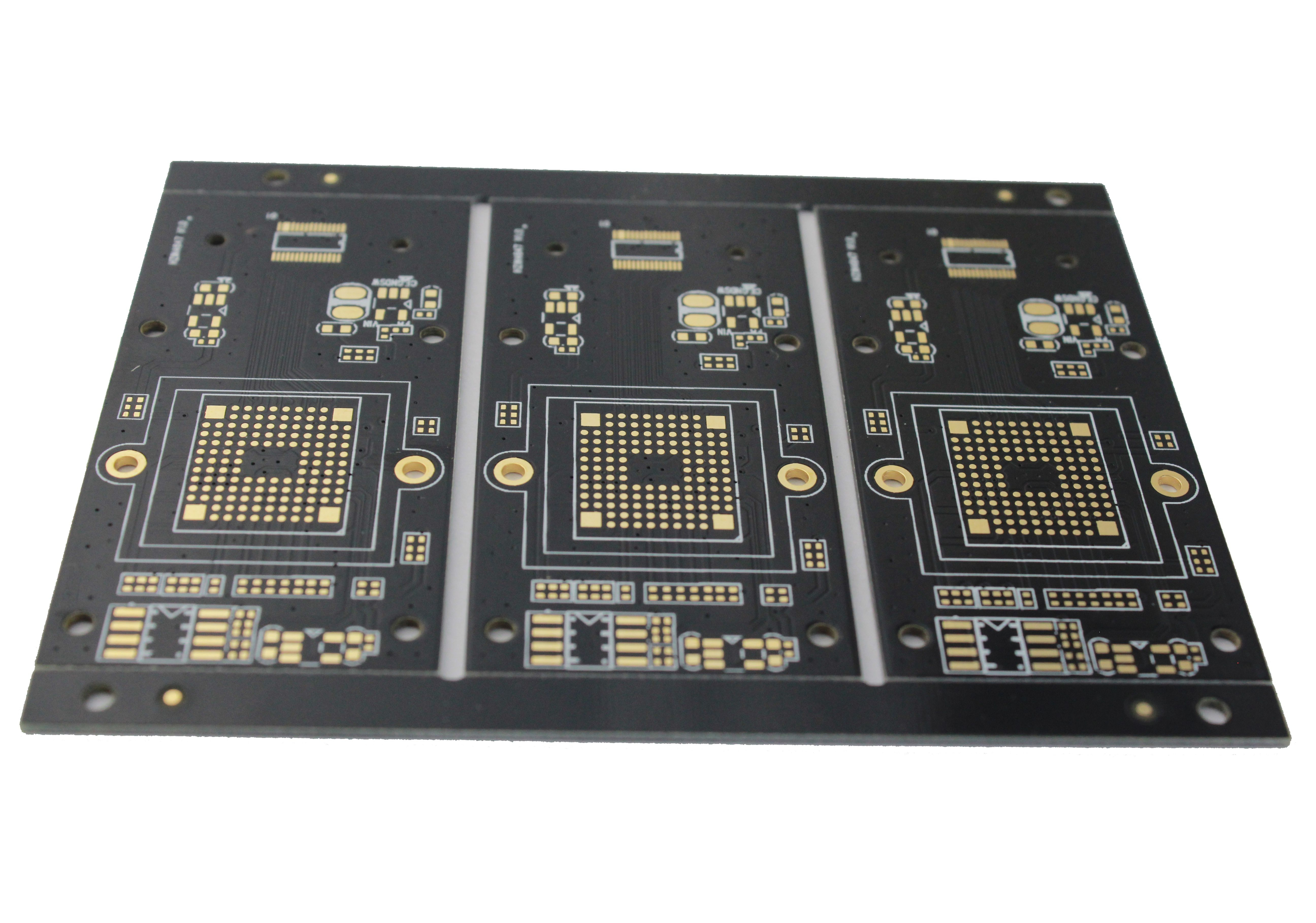
- Package Substrate (IC Substrate): Serving as a bridge between the chip and PCB, it employs high-density wiring (e.g., ABF/BT substrate) to connect micron-scale pads to PCBs while providing mechanical support and thermal pathways.
What Are Functions of IC Circuit Board?
Functions of IC Circuit Board:
- Mechanical Support and Fixation: Provides a stable physical installation platform for integrated circuit chips, resistors, capacitors, and other electronic components, ensuring they remain securely positioned and undamaged during device operation.
- Electrical Connection and Signal Transmission: Enables electrical interconnection between components through surface-etched metal traces and multi-layer wiring structures, efficiently transmitting power, control signals, and data signals.
- Thermal Management: Utilizes substrate materials (such as ceramic or metal substrates) or built-in thermal structures (like thermal vias or heat sinks) to rapidly dissipate heat generated by chips, maintaining stable operating temperatures.
- Environmental Protection: Employs packaging structures (e.g., DIP, QFN) and solder mask layers (green/red oil) to shield internal circuits from environmental hazards such as moisture, dust, and chemical corrosion.
- Interface and External Connection: Offers standardized interfaces (e.g., pins, solder balls, connectors) for reliable electrical connections to external circuits, power supplies, or other devices.
- Functional Integration and Modularity: Integrates core circuit modules including transistors, logic gates, memory cells, etc., supporting computation, control, storage, and other essential functions of electronic devices while enabling highly compact designs.
- Cost Control and Scalable Production: Reduces manufacturing costs per unit through standardized designs, batch production, and automated assembly, while improving production efficiency and yield rates.
- Signal Integrity Assurance: Minimizes signal loss, crosstalk, and electromagnetic interference during transmission via precision wiring design, impedance matching, and shielding measures, ensuring stable high-speed signal transmission.
What Are Applications of IC Board?
Applications of IC Board:
- Tablet PC Image Processing
- Smart Home Appliance Control
- 5G Base Station Signal Transmission
- Router Network Data Forwarding
- Autonomous Driving Environmental Perception
- Vehicle Battery Management System
- Medical Imaging Equipment Diagnosis
- Industrial Robot Motion Control
- Aerospace Navigation and Positioning
- Data Center High-Performance Computing
- Smart Grid Energy Monitoring
- Solar Power Generation Conversion
- Smart Meter Remote Meter Reading
- Medical Life Support System
- Industrial Sensor Data Acquisition
- Satellite Communication Signal Processing
- Aircraft Flight Control System
- Server Storage Chip Management
- Consumer Electronics Audio Processing
IC PCB Board Design Specification
| Design Parameter | Typical Value/Range |
| Layer Count | 2–40+ layers (depending on complexity) |
| Board Thickness | 0.2–8.0mm (standard FR4: 1.6mm) |
| Substrate Type | FR4, High-Frequency Materials (e.g., Rogers/Arlon) |
| Minimum Trace Width | 0.05–0.1mm (outer layers) |
| Minimum Trace Spacing | 0.05–0.1mm |
| Single-Ended Impedance | 50±5Ω |
| Differential Impedance | 90–100Ω (e.g., USB2.0/HDMI) |
| PTH Diameter | ≥0.10mm (mechanical drilling) |
| Microvia Diameter | 0.04–0.10mm (laser drilling) |
| Pad Diameter | Hole size +0.1–0.3mm (minimum annular ring) |
| Surface Finish | ENIG, Immersion Tin, Immersion Silver |
| Dielectric Constant (εᵣ) | 4.2–4.5 (FR4) |
| Signal Layer Count | 3–6 layers (typical multi-layer boards) |
| Board Size | ≤508×610mm (maximum) |
| Layer Alignment Accuracy | ±0.1mm |
| Thickness Tolerance | ±8% |
How to Design A IC Board?
1. Requirement Analysis and Specification Formulation
- Scene-specific demand refinement: For consumer electronics (e.g., smartphone main frequency ≥3GHz), industrial control (temperature resistance -40~125℃), automotive electronics (AEC-Q100 certification) and other scenarios, quantify specific indicators (e.g., power noise ≤2% VCC).
- Standard and regulatory alignment: Clarify IPC-A-610 soldering standards, RoHS environmental requirements, EMC/EMI testing specifications (e.g., CISPR 25), and reserve design margins to address process fluctuations.
2. Architecture Design and Planning
- Modular design strategy: Adopt IP core reuse (e.g., CPU soft core, DDR controller), define clear interface protocols (I2C/SPI/PCIe), and evaluate module-level power distribution (e.g., dynamic power proportion ≤70%).
- Process-material-package collaboration: Select substrates based on signal rate (FR4 for ≤1GHz, PTFE/ceramic for high-frequency scenarios), match packaging forms (QFN/BGA), and verify thermo-mechanical reliability (e.g., CTE matching).
3. Circuit Design and Simulation
- Mixed-signal design: Distinguish digital/analog regions, adopt isolation strips (≥3 times line width) to reduce crosstalk; analog circuits require separate power/ground planes and decoupling capacitor gradients (1μF+10nF).
- Multidimensional simulation verification: Pre-simulation includes functional verification (Verilog-AMS models), timing analysis (setup/hold checks), signal integrity (eye diagram margin ≥20% UI); post-simulation incorporates parasitic parameter extraction (R/C/L) to verify actual delay ≤10% of clock cycle.
4. Physical Layout Design
- Intelligent layout algorithm: Use automatic layout tools (e.g., Cadence Innovus) to optimize component positions, manually adjust critical paths (e.g., clock tree) to reduce delay; place thermally sensitive components (e.g., power transistors) near heat sinks and reserve thermal via arrays.
- Wiring rule deepening: High-speed differential pairs (e.g., USB3.0) adopt equal-length routing (error ≤5mil), spacing ≥2 times line width; power plane segmentation avoids sharp angles, copper foil thickness ≥2oz for enhanced current capacity.
5. Layout Implementation and Verification
- Advanced process adaptation: For processes below 28nm, adopt double patterning technology (DPT) to resolve lithography limits; incorporate dummy fills to improve uniformity and guard rings to suppress noise.
- Multi-round verification closed loop: After DRC/ERC/LVS checks, perform power integrity analysis (IR-Drop ≤50mV), signal integrity review (reflection/crosstalk ≤5%); modify netlists via ECO if necessary and re-verify.
6. Post-Simulation and Parameter Extraction
- Thermal-electrical coupling analysis: Use Ansys Icepak for thermal simulation, combine electrical parameters (e.g., on-resistance) to evaluate hotspot distribution; critical devices (e.g., MOSFETs) maintain junction temperature ≤125℃ with thermal allowance.
- Reliability accelerated testing: Validate long-term reliability through high-temperature operating life (HTOL), temperature cycling (TC); package-level tests (e.g., solder ball shear force ≥10N) ensure mechanical strength.
7. Manufacturing File Output
- Process file standardization: Generate manufacturing instructions including layer stack structures (layer thickness/material), impedance control tables, drilling parameters (hole diameter/tolerance), and confirm process capabilities (e.g., minimum line width/spacing) with foundries.
- Supply chain full-process management: Establish BOM lists, audit supplier qualifications (e.g., ISO certification), plan SMT process parameters (temperature curves), and design test fixtures (e.g., JTAG interfaces) for mass production testing.
8. Testing and Validation
- Multi-stage testing strategy: Prototype phase includes functional testing (e.g., I/O level verification), boundary scan (JTAG chain detection); mass production employs statistical process control (SPC) to monitor yield, and samples undergo environmental stress tests (e.g., 85℃/85%RH constant humidity).
- Document digital archiving: Use PDM systems to manage design files (layouts/simulation reports), test data (eye diagrams/temperature rise curves), and change records, supporting traceability and iterative optimization.
IC Board Assembly Processes
1. Wafer Dicing and Selection
- Dicing Technology Evolution: Mechanical blade dicing uses diamond-coated blades for wafers over 100μm, while laser dicing employs UV/IR lasers for contactless cutting of ultra-thin wafers (<100μm) and complex patterns. Post-dicing cleaning involves deionized water rinsing to remove silicon debris and UV exposure to reduce blue tape adhesion for easier die picking.
- Die Selection Process: Utilizes vacuum suction or robotic arms with high-precision vision systems to select qualified chips, rejecting edge-defective dies. Yield control integrates AOI detection for real-time feedback.
2. Die Attach
- Adhesive Systems: Conductive adhesives (e.g., silver paste) for high thermal conductivity applications, non-conductive adhesives for insulation, and solder pastes (Sn-Ag-Cu) for high-temperature reliability. Curing profiles match material properties—thermal curing at 175–185°C or UV curing for 90–120 seconds.
- Precision Alignment: High-precision die bonders achieve ±0.05mm positional accuracy using dual-vision systems and pressure sensors to control bonding force, preventing chip damage.
3. Wire Bonding
- Material Selection: Gold wires (20–30μm) for high-frequency reliability, aluminum wires for cost efficiency (lower strength), and copper wires with nitrogen protection for oxidation resistance. Bonding methods include thermosonic (gold) or ultrasonic (aluminum) techniques, ensuring bond strength ≥5g without non-stick bonds.
- Process Optimization: Bonding parameters (force, temperature, time) are optimized via DOE experiments. X-ray inspection confirms void-free bonds, while SEM analyzes microstructural integrity.
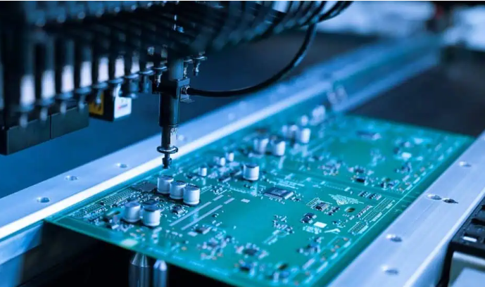
4. Surface Mount Technology (SMT)
- Solder Paste Printing: Stencil printing maintains solder paste thickness deviation ≤±15%, with SPI verification for uniformity. High-density PCBs use stepped stencils (0.03mm local thickening) to compensate solder volume.
- Placement and Reflow: High-speed pick-and-place machines achieve 0201 component placement accuracy ±25μm. Reflow uses 10-zone nitrogen-protected furnaces, peak temperature 235–245°C for 40–60 seconds, monitored by thermocouples. AOI checks 11 solder joint criteria, with 3D detection for BGA shadow elimination.
5. Through-Hole Technology (THT)
- Wave Soldering: Turbulent waves break through oxidation layers, while smooth waves form solder joints. Process parameters: 2–5 seconds at 240–260°C. Flux spray systems precisely control coating volume, and preheat gradients minimize thermal shock.
- Lead Forming: DIP/PGA component leads are bent using precision dies to match PCB hole dimensions, with tolerance ≤0.1mm.
6. Encapsulation and Protection
- Material Selection: Plastic molding (epoxy) for cost efficiency (limited thermal resistance), ceramic for high-frequency/high-power, and metal for optimal thermal conductivity. Underfill materials use capillary action to fill BGA gaps, eliminating thermal stress.
- Process Refinement: Transfer molding pressure 10–20MPa, curing time 90–120 seconds. Vacuum degassing reduces encapsulation voids, with solder paste oxidation <1% for enhanced joint reliability.
7. Testing and Validation
- Electrical Testing: ICT checks opens/shorts, flying probe tests cover high-density boards, and functional tests verify system performance. DC tests measure terminal voltage/current, while AC tests evaluate gain/distortion.
- Reliability Testing: High-temperature/humidity (85°C/85% RH), thermal cycling (-40°C to 125°C), and vibration (5–2000Hz) screen for latent defects. AEC-Q standards apply to automotive electronics, supporting 2000V/200A high-power testing.
8. Quality Control Essentials
- Statistical Process Control: SPC charts monitor solder paste thickness, placement accuracy, and soldering temperature. Process capability indices (Cp/Cpk) assess stability via Minitab visualization.
- Traceability System: Batch records include wafer lot IDs, equipment parameters, and operator info, stored in cloud systems for 10-year traceability. ESD protection maintains workstation grounding resistance <1Ω.
9. Common Issues and Solutions
- Solder Joint Defects: Reflow profile optimization with extended preheat and nitrogen protection reduces oxidation. Metallographic analysis ensures IMC layer thickness ≤5μm for reliability.
- Die Warpage Control: Substrate warpage <0.75% using high-Tg materials. Vacuum degassing and <1% solder paste oxidation minimize voids.
10. Environmental Compliance
- Lead-Free Processes: Compliant with RoHS using Sn-Ag-Cu solder (lead content <1000ppm). Waste management includes segregated recycling of solder dross and adhesive waste, with emissions treated via activated carbon adsorption and combustion.
- Circular Economy: Metal/plastic waste repurposed into recycled products; agricultural waste converted to organic fertilizer or bioenergy for full lifecycle sustainability.
Why Choose EBest Circuit (Best Technology) as IC Board Assembly Manufacturer?
Reasons why choose us as IC board assembly manufacturer:
- Proven Industry Expertise: With 15 years of deep expertise in IC board assembly, serving over 200 Fortune 500 companies globally. Certified success stories across automotive electronics (AEC-Q100), industrial control, and consumer electronics, empowering client value upgrades through professional experience.
- 5-Year Warranty Assurance: Backed by industry-leading warranty terms, providing clients with long-term reliability confidence without compromising service quality.
- Cost Optimization: Leverage economies of scale and intelligent supply chain optimization to reduce raw material costs by 15%-20%. Combined with lean production models, this minimizes process waste, delivering highly competitive pricing that boosts client profit margins.
- Rigorous Quality Control: Implement AOI+X-ray dual-inspection systems for 100% solder joint verification. SPC statistical process control ensures critical parameters achieve Cp/Cpk ≥1.67, maintaining yield rates above 99.8% to slash post-sale repair costs and return risks.
- Lightning-Fast Delivery: Innovative “3-5-7” rapid delivery system—3 days for prototype validation, 5 days for pilot production, and 7 days for mass production launch. Dynamic capacity allocation reduces emergency order lead times by 40%, empowering clients to seize market opportunities swiftly.
- Comprehensive Technical Support: Dedicated 20-member engineering team provides end-to-end technical accompaniment from DFM design to mass production troubleshooting. Capable of handling ultra-precision processes like 0201 component placement and 01005 micro-resistor welding, ensuring 100% design realizability.
- Global Environmental Compliance: Full compliance with RoHS 2.0 and REACH standards using lead-free solder (Pb content <1000ppm) and recyclable materials. Certified under ISO 14001 environmental management system, facilitating smooth customs clearance for European and American markets.
- Flexible Customized Production: Supports agile switching from low-MOQ (as low as 50 pieces) multi-variety batches to large-scale production. Smart material management systems enable precise BOM traceability, meeting diverse customization demands.
- Comprehensive Reliability Validation: Rigorous testing includes high-temperature/humidity (85°C/85%RH), thermal shock (-40°C~125°C for 1000 cycles), and mechanical vibration (5-2000Hz) to extend product lifespan by over 30% and enhance market reputation.
Welcome to contact us if you have any request for IC board assembly: sales@bestpcbs.com.