High-Density Interconnect (HDI) PCBs are revolutionizing the electronics industry with their advanced capabilities and compact designs. As technology continues to evolve, the demand for smaller, faster, and more efficient electronic devices has led to the widespread adoption of HDI PCBs.
What is Definition of HDI PCB?
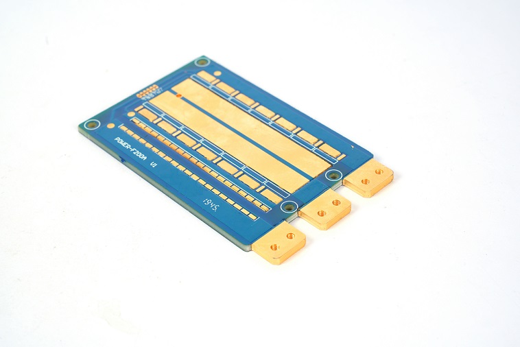
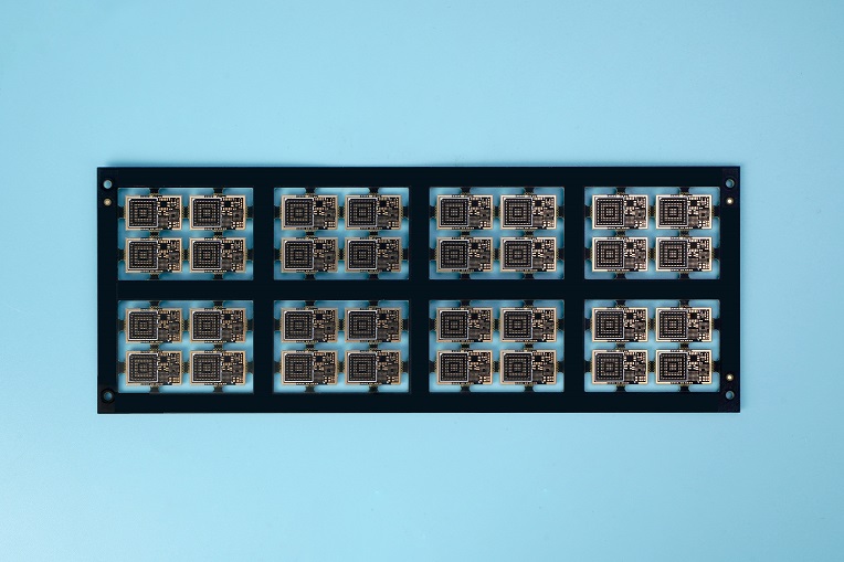
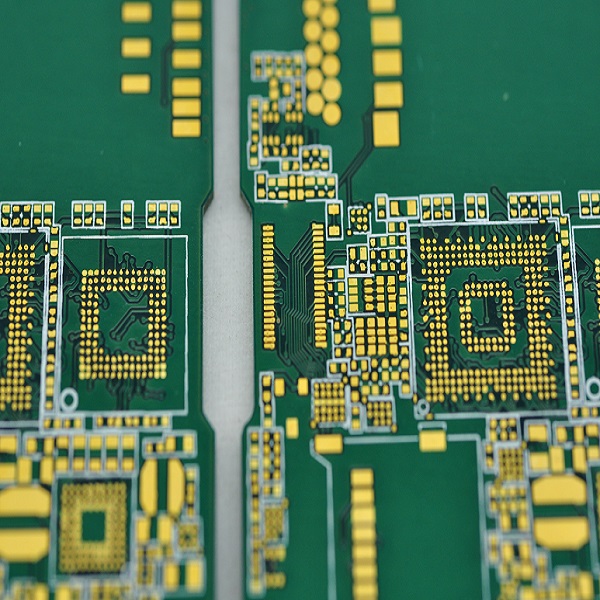
HDI board refers to High Density Interconnect, that is, high density interconnect board, which is a relatively new technology developed by the PCB industry at the end of the 20th century.
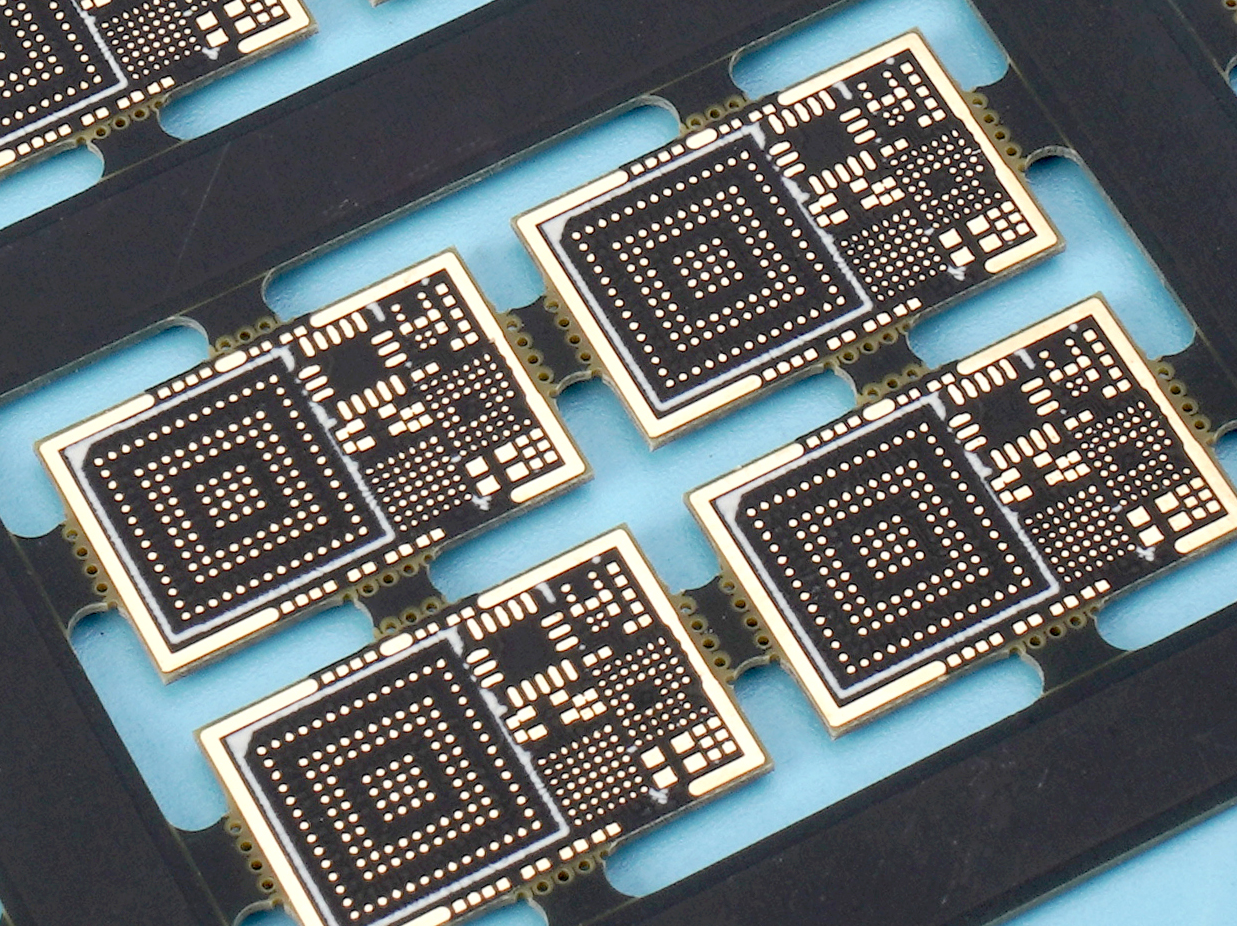
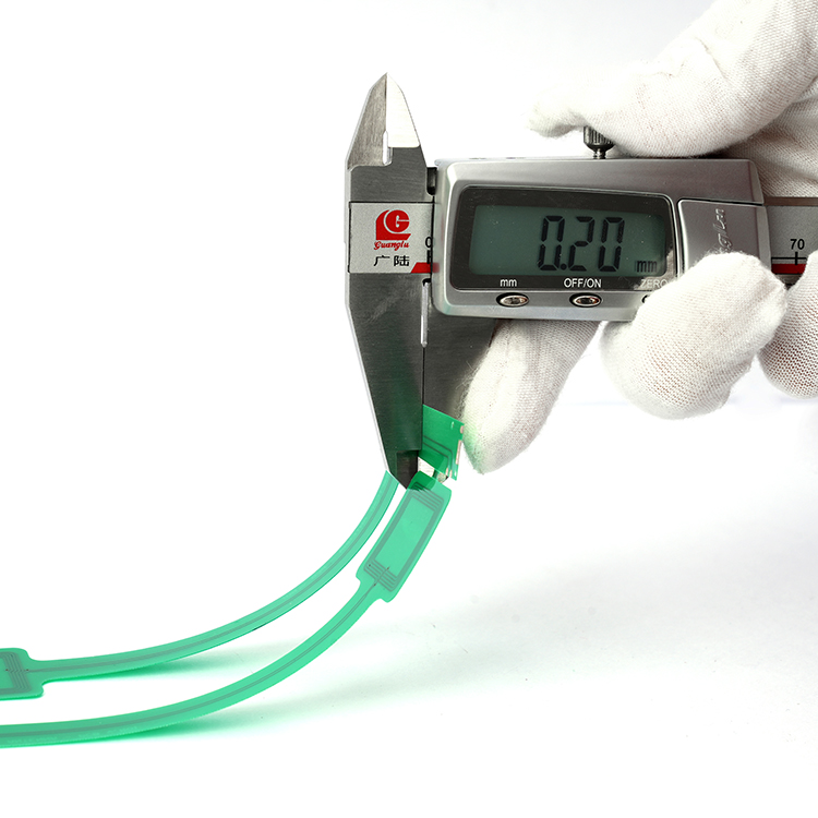
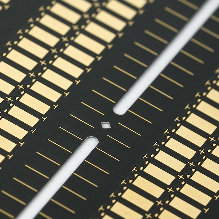
The drilling of the traditional PCB board is affected by the drilling tool, and when the drilling aperture reaches 0.15mm, the cost is already very high, and it is difficult to improve again. The drilling of HDI board no longer relies on traditional mechanical drilling, but uses laser drilling technology. (This is why it is sometimes called a laser plate.) The hole diameter of the HDI board is generally 3-5mil (0.076-0.127mm), the line width is generally 3-4mil(0.076-0.10mm), the size of the pad can be greatly reduced, so more line distribution can be obtained within the unit area, and the high-density interconnection comes from this.
Smaller device spacing, more I/O pins and embedded passive devices Larger ASiCs and FPGAs with increasingly shorter rise times and higher frequencies all require smaller PCB feature sizes, which is driving a strong demand for HDI/ micro through-holes. The typical high density interconnector designs are including:
- 1+N+1
- 2+N+2
- 3+N+3
- 4+N+4
What are the benefits of HDI PCB?
HDI is a compact circuit board designed for small volume users. Compared with ordinary FR4 PCB, the most significant feature of HDI is the high wiring density, and the difference between the two is mainly reflected in the following three aspects.
1. HDI is smaller and lighter
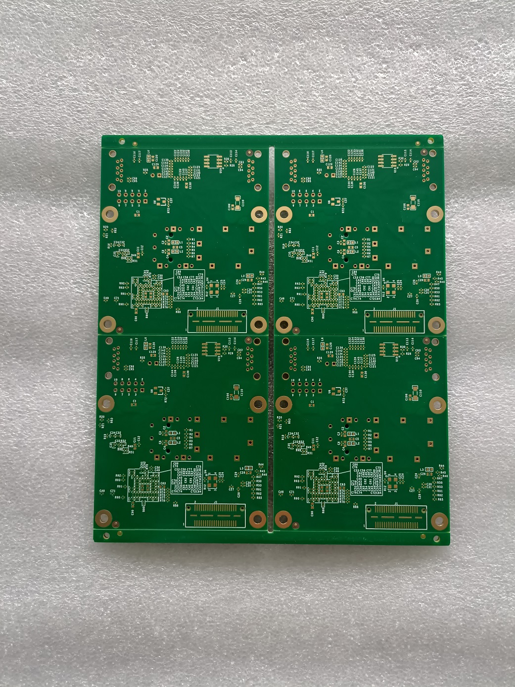
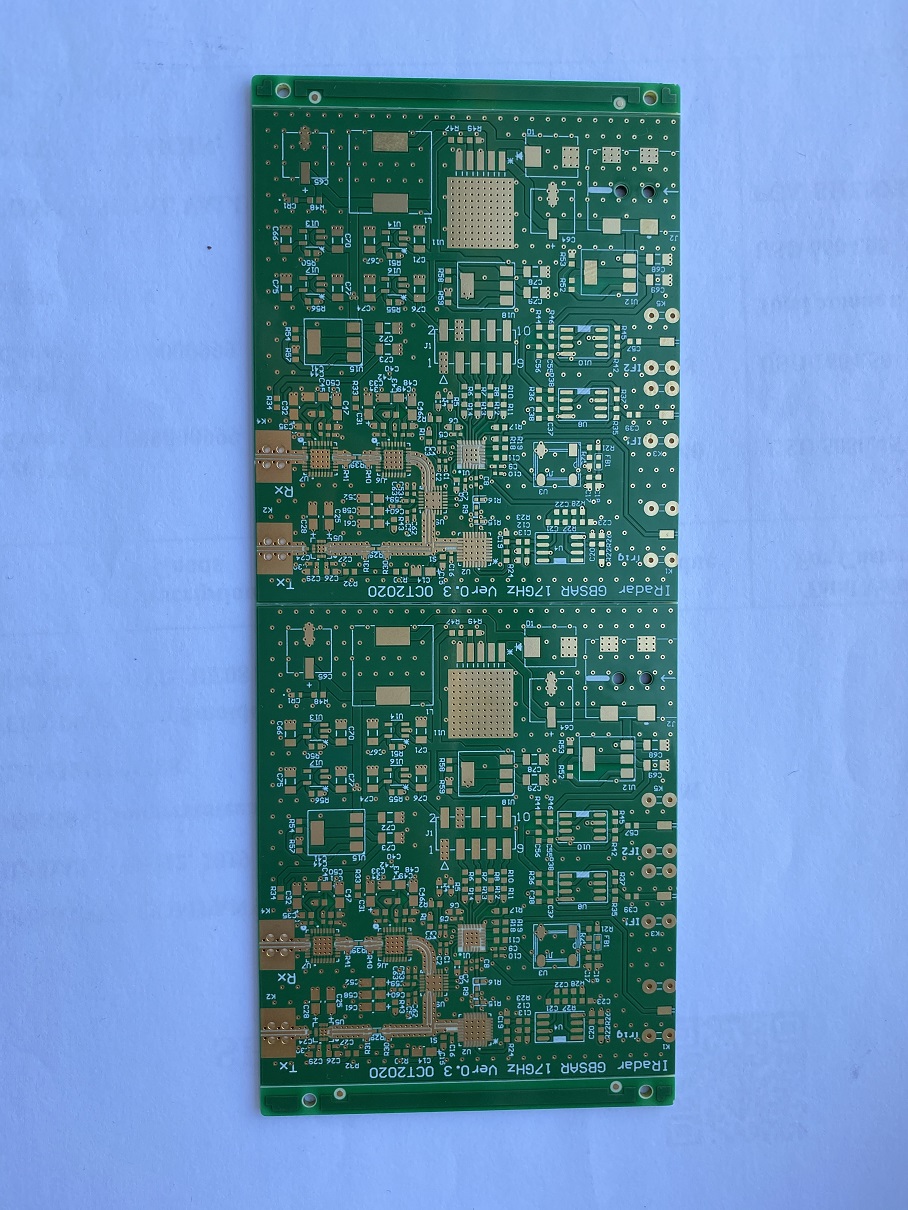
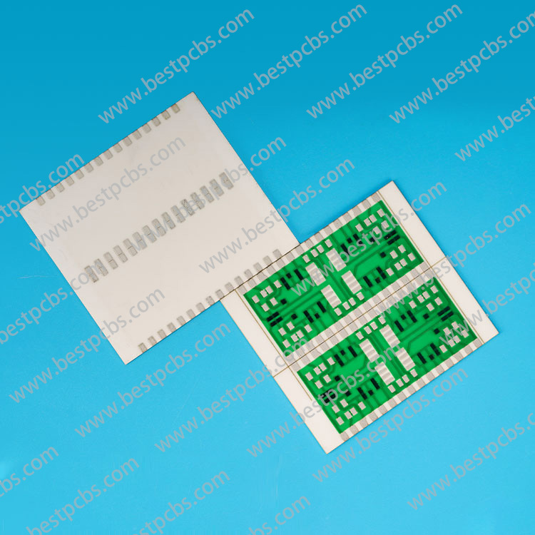
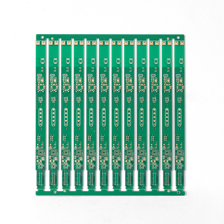
HDI board is a traditional dual panel as the core board, through continuous stacking layer by layer. This kind of circuit board made by continuous layering is also called Build-up Multilayer (BUM). Compared with traditional circuit boards, HDI circuit boards have the advantages of “light, thin, short and small”.
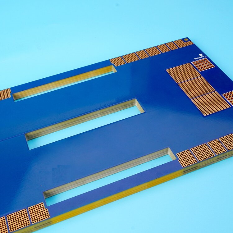
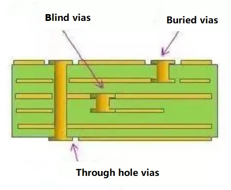
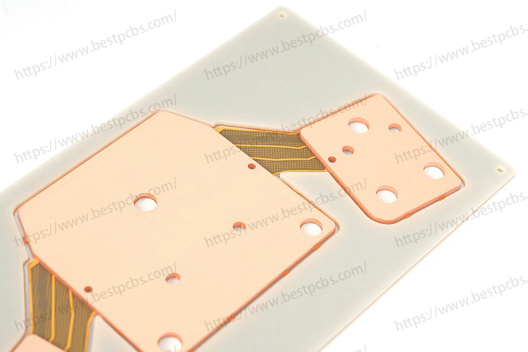
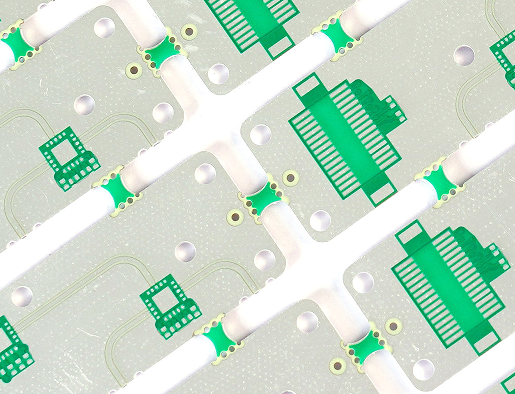
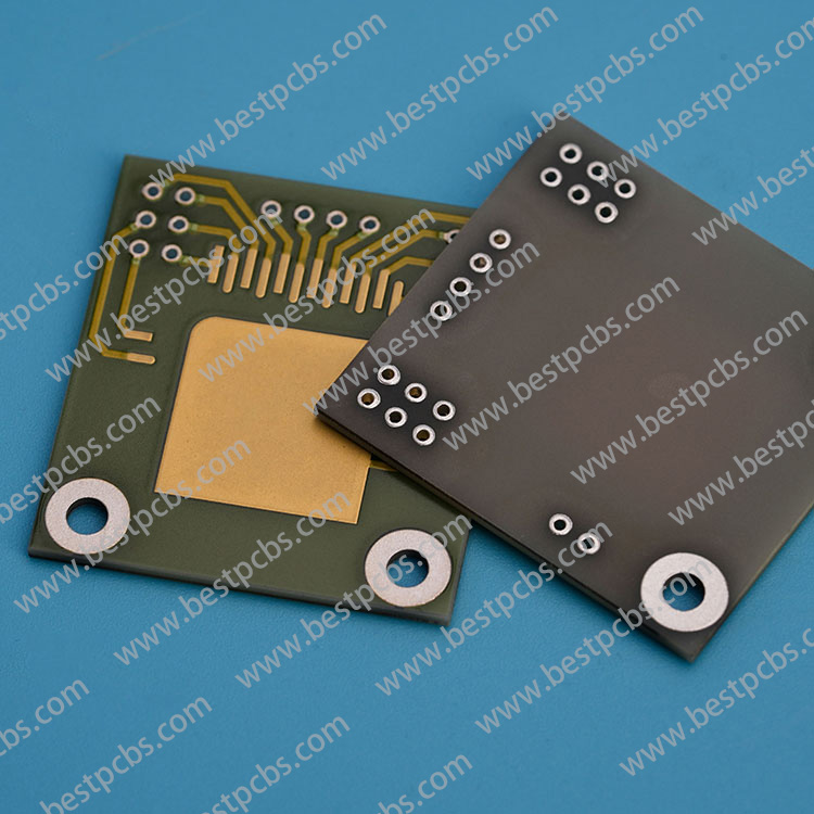
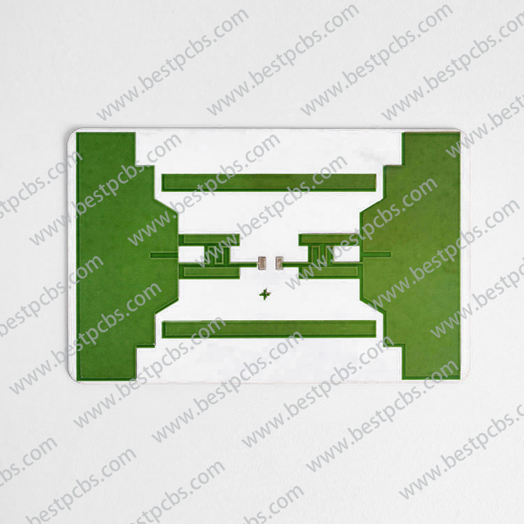
The electrical interconnection between the HDI board is realized through the conductive through hole, buried hole and blind hole connection, its structure is different from the common multi-layer circuit board, and a large number of micro-buried blind holes are used in HDI board. HDI uses direct laser drilling, while standard PCBS usually use mechanical drilling, so the number of layers and aspect ratio tend to be reduced.
The high density of HDI board is mainly reflected in the hole, line, pad density, and layer thickness.
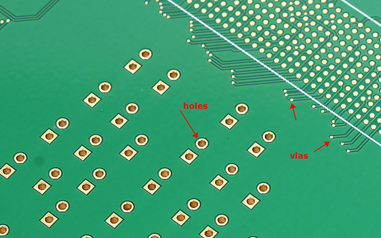
● Micro-via hole
The HDI board contains the design of micro-pilot holes such as blind holes, which is mainly reflected in the micro-hole formation technology with a diameter less than 150um, and the high requirements of cost, production efficiency and hole position precision control. In the traditional multilayer circuit board, there are only through holes and no tiny buried blind holes.
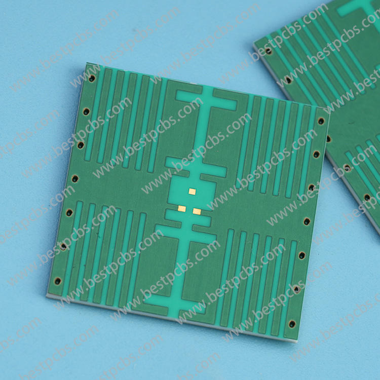
● Fine line width and line distance
Its main performance in the wire defects and wire surface roughness requirements are more and more stringent. Generally, the line width and line distance do not exceed 76.2um.
● High pad density
The density of welded contacts is greater than 50 per square centimeter.
● Thinning of medium thickness
It is mainly manifested in the trend of the thickness of the interlayer medium to 80um and below, and the thickness uniformity requirements are becoming more and more stringent, especially for high-density plates and packaging substrates with characteristic impedance control.
2. Better electrical performance
HDI not only enables end-product designs to be miniaturized, but also to meet higher standards of electronic performance and efficiency at the same time.
The increased interconnect density of HDI allows for increased signal strength and improved reliability. In addition, the HDI board has better improvement for RF interference, electromagnetic wave interference, electrostatic discharge, heat conduction and so on. HDI also uses full digital signal process control (DSP) technology and a number of patented technologies, with a full range of load adaptability and strong short-term overload capability.
3. The HDI board has very high requirements for buried holes
It can be seen from the above that whether it is the volume of the board, or the electrical performance, HDI is better than ordinary PCB. Where the coin has two sides, the other side of HDI is as a high-end PCB manufacturing, its manufacturing threshold and process difficulty are much higher than ordinary PCB, and there are more problems to pay attention to when producing – especially the buried hole jack.
What are the basic parameters of HDI PCB?
HDI PCB has greater different with normal FR4 PCB, from the stack up, material selection, manufacturing and cost. So, it is vital to understanding the basic parameters of a high-density interconnect board before start your designing trip. The standard parameters of HDI board mainly include the following aspects:
- Numbers of layers
Generally, the number of layers of HDI board is 4-20 layers, and the high-end HDI board can reach to 40-50 layers.
- Line width/spacing
Due to the HDI PCB are always used in high-end applications, their line width and spacing are usually very strict, and the common requirement is that the line width/spacing is 4/4mil (0.1mm), or even smaller.
- Blind hole, buried hole, bus
These are one of the characteristics of the HDI board, blind hole and buried hole can reduce the area of the circuit board, make your design more density, and the bus enable to improve the signal transmission rate of the PCB.
- Board thickness
The board thickness of HDI board is usually range from 0.8 to 3.2mm, of which 1.6mm is the most common thickness.
- Pad
The pad on the HDI board is generally very small, and the common pad size is 0.2mm to 0.5mm. Different factory has different capabilities, it is best to ask your supplier or manufacturer to get a manufacturing capability document.
- Impedance control
For high-speed signal transmission circuits, the impedance control of the HDI board is very important, and the requirements are very strict. It is needed to tell your vendor if your HDI board will be used in high-speed devices.
- Material
The main materials of HDI board are FR4, BT, PI, PET, etc. Different materials can meet different requirements.
This is the end of this sharing, contact us today to learn more about our HDI PCB solutions and how we can help you achieve your technological goals. In our next chapter, we will introduce the manufacturing process and methods of HDI boards, let me know if you are interested in it.