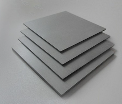
Rogers RT Duroid 5880 is a high-frequency laminate specifically designed for applications where precision and low signal loss are critical. The substrate is a composite material known for its excellent performance in RF and microwave circuits. It uses a PTFE (polytetrafluoroethylene) base reinforced with glass microfibers.
The use of glass microfiber ensures the material is durable but lightweight, making it suitable for applications in which weight is a factor. Its composition is perfect for projects where high-frequency signals are involved. From defense systems to automotive radar, RT Duroid 5880 is a reliable choice. It has become the go-to substrate for engineers and designers looking for efficiency, precision, and durability.
Composition of Rogers RT/duroid 5880
RT Duroid 5880 is composed of PTFE (polytetrafluoroethylene) combined with glass microfiber. PTFE provides a low dissipation factor, which reduces signal loss. This is important for maintaining high performance in RF and microwave applications. Glass microfiber reinforces the material, make it stronger without adding unnecessary weight. The composition also includes copper cladding, which is typically laminated on both sides. The copper layer helps with conductivity, ensuring signals travel efficiently across the board.
The unique combination of PTFE and glass microfiber gives RT Duroid 5880 its excellent mechanical stability. It also minimizes the effect of temperature changes, which is critical for high-frequency circuits. As a result, the material can handle extreme temperatures without affecting the performance of the PCB.
RT/duroid 5880 Specifications
The following table highlights the important specifications of Rogers RT Duroid 5880. These specs reflect the high performance of RT Duroid 5880 for complex RF and microwave tasks.
Property
Value
Dielectric Constant (Dk)
2.20 (±0.02)
Dissipation Factor (Df)
0.0004 (measured at 10 GHz)
Thermal Conductivity
0.20 W/m/K
Operating Temperature Range
-55°C to +150°C
Water Absorption
0.02%
Volume Resistivity
1.7 x 10^9 MΩ·cm (minimum)
Surface Resistivity
1.4 x 10^8 MΩ (minimum)
Coefficient of Thermal Expansion (CTE)
46 ppm/°C (in X-Y axis)
Tensile Strength
10.3 MPa
Flammability
UL 94 V-0
Peel Strength
5.0 N/mm (after soldering)
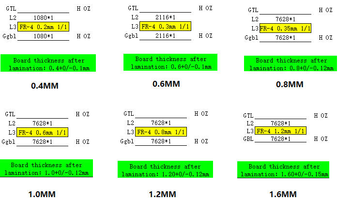
RT/duroid 5880 Thickness
RT Duroid 5880 comes in various thicknesses. Engineers can choose the right thickness depending on their project’s needs. Rogers RT/duroid 5880 laminate is commercially available in sheet stock and roll stock forms in a range of thicknesses. Here’s a list of the standard thicknesses available:
Available sheet sizes:
304.8 x 457.2 mm
457.2 x 609.6 mm
609.6 x 914.4 mm
Standard thickness:
0.127 mm (5 mils)
0.254 mm (10 mils)
0.381 mm (15 mils)
0.508 mm (20 mils)
0.787 mm (31 mils)
1.524 mm (60 mils)
3.175 mm (125 mils)
Available roll widths:
304.8 mm
609.6 mm
1219.2 mm
Standard roll length: 76.2 meters
Thickness range: 0.127 mm to 1.575 mm
RO5880 RF PCB Advantages
Rogers RT Duroid 5880 has a lot of strengths when used in RF and microwave PCB projects:
Minimal Signal Loss
With a low dissipation factor of 0.0004, it reduces signal loss, which is very helpful for high-frequency systems like radar or satellite communications.
Strong Stability
It holds up well under temperature changes and in humid environments, keeping circuits running smoothly even in tough conditions.
Reliable Electrical Properties
The dielectric constant of 2.20 remains stable over a range of frequencies. This helps keep circuits working consistently without interference or signal issues.
Heat Tolerance
It withstands heat up to 150°C, making it a good choice for systems that need to handle higher temperatures.
Low Moisture Absorption
With only 0.02% water absorption, the material works well in damp environments. Outdoor systems like antennas benefit from this.
Ease of Manufacturing
The material is easy to work with during production, which keeps costs lower and speeds up manufacturing.
Chemical Resistance
The PTFE base resists damage from chemicals and solvents, making the material last longer in harsh environments like aerospace and industrial applications.
Typical Applications of High-Frequency PCB
High-frequency PCBs built with Rogers RT Duroid 5880 serve important roles across many industries:
Aerospace – used in radar, satellite, and navigation systems, RT Duroid 5880 supports reliable communication and tracking, even in high-pressure environments.
Telecommunications – in mobile networks, base stations, and antennas, high-frequency PCBs help maintain clear and fast data transmission, supporting the backbone of communication systems.
Medical Devices – MRI machines, wireless health monitors, and other equipment use high-frequency PCBs to keep medical data accurate and systems working seamlessly.
Defense – communication gear, and electronic warfare systems.
Automotive Systems – advanced driver assistance systems (ADAS) and vehicle radar depend on high-frequency PCBs for real-time data, making roads safer for everyone.
Satellite Communication – RT Duroid 5880 is frequently used in satellite systems where strong signal transmission over long distances is crucial for communication networks.
Common-Used High Frequency PCB Materials in EBest Circuit (Best Technology)
At EBest Circuit (Best Technology), we use a range of top-quality materials for high-frequency PCBs, depending on the project’s needs. Some of the most popular materials include:
Material
Dielectric Constant (Dk)
Loss Tangent (Df)
Key Features
Rogers RO4003C
3.38
0.0027
Low loss, excellent thermal stability, ideal for RF applications.
Rogers RO4350
3.48
0.0043
Low loss, high thermal conductivity, suitable for microwave applications.
RT/Duroid RO5880
2.94
0.0037
Very low loss, excellent performance at high frequencies, good for multilayer designs.
N4000-13
3.0
0.009
Good thermal stability, low moisture absorption, designed for high-frequency applications.
Taconic RF-60A
6.15
0.0027
High dielectric constant, low loss, suitable for low-loss RF and microwave applications.
Each material brings different strengths for specific applications, giving you the best options for your project.
Discuss Your High Frequency PCB Project with Us Today
If you have a high-frequency PCB project in mind, reach out to us. We’re experienced in creating high-quality PCBs that meet your exact specifications. Whether you need RF, microwave, or other types of high-frequency boards, we’ll make sure your project runs smoothly. Contact us at sales@www.bestpcbs.com today, and we’ll help you turn your plans into reality.
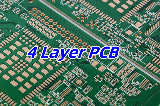
A 4 layer PCB is a type of circuit board that consists of four distinct layers of conductive material. Each layer serves a specific function. The layers typically include two signal layers, one ground (GND) layer, and one power (VCC) layer. Generally, through holes, buried holes, and blind holes are used to connect the internal layers. There are more buried and blind holes than 2 layer PCB boards. In addition, try not to run signal track on the two layers of VCC and GND. A 4 layer PCB offers more complex designs, better signal integrity compared to simpler designs.
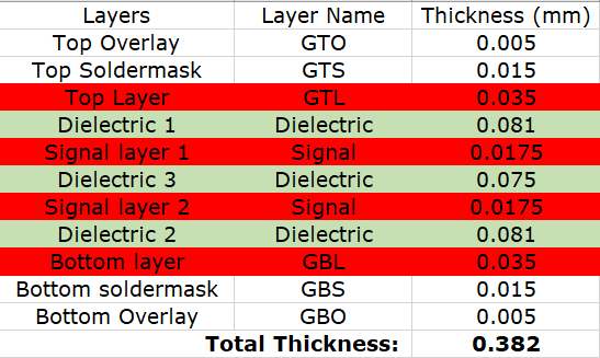
4 Layer PCB Stack-up
The typical stack-up configuration is as follows:
Top Layer (Signal Layer): This layer carries signals and connections.
Inner Layer 1 (Ground Plane): This layer serves as a reference for signal return paths, reducing noise and interference.
Inner Layer 2 (Power Plane): This layer distributes power to various components on the PCB.
Bottom Layer (Signal Layer): Like the top layer, it carries additional signals and connections.
4 layer PCB Stack up Options
Generally, there are three main categories for preferred stack-up solutions for 4 layer PCBs:
Solution 1: The standard layer setup for common 4 layer PCBs.
TOP (signal layer)
GND1 (ground layer)
PWR1 (power layer)
BOT (signal layer)
Solution 2: Suitable for situations where key components are laid out on the BOTTOM
layer or key signals are routed on the bottom layer; generally applicable under certain restrictions.
TOP (signal layer)
PWR1 (power layer)
GND1 (ground layer)
BOT (signal layer)
Solution 3: Suitable for PCBs primarily using through-hole components, commonly
used where the power is routed in layer S2, and the BOTTOM layer serves as a ground plane, thereby forming a shielding cavity.
GND1 (ground layer)
S1 (signal layer)
S2 (signal layer)
PWR1 (power layer)
Top LayerG1G2Bottom Layer
4 Layer PCB Thickness
The thickness of a 4 layer PCB can vary depending on the design requirements. Generally, a standard 4 layer PCB thickness ranges from 0.4mm to 1.6mm. The total thickness is determined by the materials used and the copper weight on each layer. A thicker PCB can offer better thermal management and mechanical stability, making it suitable for high-power applications. Here are the 4 layer PCB thickness with different thickness in EBest Circuit (Best Technology):
4 Layer PCB Manufacturing Process
Cutting material and grinding → drilling positioning holes → inner layer circuit → inner layer etching → inspection → black oxide → lamination → drilling → electroless copper → outer layer circuit → tin plating, etching tin removal → secondary drilling → inspection →print solder mask→Gold-plated→Hot air leveling→print silkscreen→routing outline→Test→Inspection
Ground Plane Design in 4 Layer PCB
The ground plane in a 4 layer PCB is essential to ensuring good performance and signal integrity. Here’s how to design an effective ground plane:
1. Purpose of the Ground Plane
Reference Point: It provides a stable reference for signals, reducing noise and improving signal integrity.
Return Path: It acts as a low-resistance return path for signals, minimizing electromagnetic interference (EMI).
2. Placement in Stack-up
Typically, the ground plane is placed as one of the inner layers, often Inner Layer 1. This positioning helps shield signals on the top and bottom layers.
3. Continuous Ground Plane
Aim for a solid, uninterrupted ground plane. Breaks or cuts can introduce impedance and increase noise.
4. Vias and Connections
Use vias to connect components to the ground plane. Ensure that vias are placed close to component pads to minimize inductance.
Consider using multiple vias for high-current paths to distribute the current effectively.
5. Thermal and Electrical Considerations
Use thermal vias if heat dissipation is a concern. Place them near high-power components to spread heat away from sensitive areas. Ensure that the ground plane is thick enough to handle the expected current loads without excessive voltage drop.
6. Control EMI
Keep the ground plane as large as possible to effectively shield signals from external interference.
Route high-speed signals away from ground plane edges to minimize crosstalk.
7. Simulation and Testing
Use simulation tools to analyze the ground plane’s performance. Check for potential issues such as ground loops or noise.
After fabrication, test the PCB to ensure that the ground plane functions as intended, with minimal interference.
What is the Advantage of a 4 Layer PCB Over a 2 Layer PCB?
While 2-layer PCB boards have their advantages, multi-layer designs are more beneficial for some applications. Today EBest Circuit (Best Technology) will introduce the difference between 2-layer PCB board and 4 layer PCB.
1. A 4 layer PCB has an inner layer, which is laminated with PP and copper foil on both sides during the lamination process. This is pressed under high temperature and high pressure to form a multilayer board. Some circuits on the PCB 4 layer board are etched through the inner layer and pressed; the 2 layer PCB can be directly cut and drilled after production.
2. The 4 layer PCB is made of four layers of fiberglass, which can reduce the cost of the PCB, but the production efficiency is lower than that of the 2 layer PCB.
3. It is difficult for most people to distinguish a 4 layer PCB by observing the cross-section of the circuit board, but it can be identified by looking at the vias. If the same vias can be found on both sides of the PCB, or if the motherboard or graphics card is facing a light source and the vias do not allow light to pass through, then it is a 4 layer PCB.
4. The PCB 4 layer board has dense routing, with the top layer being the front and the bottom layer being the back.
5. The PCB 4 layer board can distribute wiring among multiple layers, which increases design flexibility and allows better control of differential impedance, single-ended impedance, and improved output for certain signal frequencies.
How to Design a 4 Layer PCB?
When designing a 4 layer PCB, it is important to differentiate between the power layer and the signal layer. The signal layer is a positive output, while the power layer is a negative output. This means that lines drawn on the signal layer will result in actual copper traces, whereas lines drawn on the power layer indicate the removal of copper. Essentially, drawing lines on the power layer corresponds to removing copper, while drawing lines on the signal layer represents creating copper traces. Therefore, when designing the power layer, you can use lines to divide the copper area into separate regions, which is known as “power segmentation.” Here is a simple design step of a 4 layer PCB:
1. Schematic Design and Drawing
2. After completing the schematic drawing, import it into the PCB software, and complete the layout with a simple arrangement.
3. Follow the plan to design the stack-up, paying attention to the following aspects:
You can generate multilayer PCB stack-ups yourself, with the default being two layers.
Choose the unit of measurement.
Pullback: This refers to the inward shrinkage of inner layers. When following the 20H rules during design, the power layer should shrink 40 to 80 mils inward compared to the reference layer. This parameter should be set accordingly.
After adding layers, name them appropriately, such as GND, etc.
4. Complete the routing operation. The negative layer contains a network copper area. Once the settings are complete, click OK.
In conclusion, a 4 layer PCB is a powerful tool in modern electronics, offering enhanced complexity, improved signal integrity, and better thermal management. By understanding its stack-up, thickness, and design guidelines, engineers can create reliable and efficient circuit boards. The advantages of 4 layer PCBs over 2 layer designs make them a preferred choice for many applications.
When you choose a 4 layer PCB, you’re investing in a technology that can support complex designs and improve overall performance. With the right design practices and advanced manufacturing capabilities, the potential for innovation is vast. Whether you’re developing consumer electronics, industrial equipment, or medical devices, a well-designed 4 layer PCB can make all the difference.
Ceramic substrate technology plays an important role in modern electronic device manufacturing. Low temperature co-fired ceramics (LTCC) and high temperature co-fired ceramics (HTCC) are two major ceramic substrate technologies, each of which has unique process characteristics and application advantages. This paper provides a comprehensive comparison of LTCC and HTCC technologies, discussing their process characteristics, material properties, performance advantages, and application areas to help engineers and researchers choose the most suitable ceramic substrate technology for their designs and applications.
1. Introduction
With the continuous progress of electronic technology, the performance and reliability of electronic components have been put forward higher requirements. Ceramic substrate technology, as one of the key materials for integrated circuits (ICs) and microwave assemblies, provides excellent electrical properties and mechanical strength. Low temperature co-fired ceramics (LTCC) and high temperature co-fired ceramics (HTCC) technologies are the two main ceramic substrate technologies, and this paper will provide an in-depth comparison of these two technologies to clarify their advantages and disadvantages as well as the applicable scenarios.
2. LTCC Technology Overview
2.1 Process
LTCC technology uses low-temperature co-fired ceramic materials, which are typically sintered at temperatures ranging from 850°C to 900°C. The process includes material preparation, printed circuitry, and a high level of sintering. The process consists of material preparation, printed circuits, lamination and co-firing. LTCC materials are usually composed of a mixture of glass and ceramic powders, which melt and fuse well at low temperatures.
2.2 Material Characterization
Low temperature co-fired ceramics (LTCC) materials have a low dielectric constant and low dielectric loss, making them suitable for high frequency applications. The conductive layer can be fabricated by screen printing technology and can support multi-layer integration, which makes LTCC perform well in space-constrained applications.
2.3 Advantages and Disadvantages Analysis
Advantages:
Multi-layer integration capability: Low temperature co-fired ceramics (LTCC) supports complex multi-layer structures, making it suitable for highly integrated circuit designs.
Cost Effectiveness: Lower sintering temperatures reduce production costs.
High-frequency performance: Excellent high-frequency characteristics for wireless communications and microwave applications.
Disadvantages:
Weak High Temperature Resistance: Not suitable for applications in high temperature environments.
Limited material selection: Compared to HTCC, LTCC has a smaller variety of materials, limiting the design for certain applications.
3. HTCC Technology Overview
3.1 Process
High temperature co-fired ceramics (HTCC) uses high-temperature co-fired ceramic materials, which are typically sintered at temperatures between 1500°C and 1600°C. HTCC materials mainly include alumina (Al₂O₃), which is capable of achieving high densities and excellent mechanical properties at high temperatures. The HTCC process involves powder preparation, molding, and sintering steps.
3.2 Material Characterization
High temperature co-fired ceramics (HTCC) materials have very high temperature resistance and chemical stability. The high temperature sintering process gives these materials excellent mechanical strength and wear resistance, making them suitable for use at high temperatures and in harsh environments. Their electrical properties are stable and suitable for high power and high frequency applications.
3.3 Analysis of Advantages and Disadvantages
Advantages:
High temperature resistance: able to withstand extremely high operating temperatures, suitable for high-temperature environments.
High mechanical strength: high strength and wear resistance, making it suitable for harsh application conditions.
Wide range of materials: support a variety of high-temperature ceramic materials to meet different application requirements.
Disadvantages:
High cost: High temperature sintering equipment and process requirements result in high production costs.
Process complexity: the need for high-temperature sintering equipment, the process is more complex.
4. Comparative analysis of LTCC and HTCC
4.1 process complexity
Low temperature co-fired ceramics (LTCC) process is relatively simple, low-temperature sintering reduces the cost of equipment and process difficulties, while HTCC requires the use of high-temperature sintering equipment, process complexity and high cost.
4.2 Material Performance
Low temperature co-fired ceramics (LTCC) materials are suitable for high-frequency and multi-layer integration applications and offer low dielectric loss, while HTCC materials offer higher mechanical strength and temperature resistance for high-temperature and high-power applications.
4.3 Comparison of Application Scenarios
LTCC (Low Temperature Co-fired Ceramics) Application Areas
1. Wireless communications:
Reason: LTCC technology has excellent high-frequency performance and low dielectric loss, which makes it suitable for radio frequency circuit (RF circuit) and microwave applications in wireless communication equipment. Its multi-layer integration capability allows the realization of complex RF circuits on a small substrate to meet the demand for high frequency and miniaturization of modern communication systems.
Application examples: mobile communication base stations, satellite communication systems, wireless sensor networks.
2. Automotive electronics:
Reason: In automotive electronic systems, LTCC can provide stable electrical performance and reliable multi-layer integration, which is suitable for in-vehicle communication modules and sensors that require high-frequency characteristics.
Application examples: automotive radar systems, in-vehicle wireless communications, automotive sensors and control units.
3. Medical devices:
Reason: LTCC technology enables highly integrated and miniaturized designs with good high-frequency performance, making it suitable for electronic components in medical instruments.
Application examples: Medical monitoring devices, medical imaging systems, implantable medical devices.
4. Consumer electronics:
Reason: LTCC’s low cost and high integration capability make it suitable for mass-produced consumer electronics such as smartphones and portable electronic devices.
Application examples: Smartphones, tablets, Bluetooth devices.
HTCC (High Temperature Co-fired Ceramics) Application Areas
1. Aerospace:
Reason: HTCC technology can withstand extremely high temperatures and harsh environmental conditions, making it ideal for high-temperature components and electronics in spacecraft and aircraft.
Application examples: High temperature sensors in spacecraft, electronic control systems in airplanes, rocket engine components.
2. Military equipment:
Reason: Military applications require high-strength, high-temperature-stable materials. HTCC’s excellent mechanical strength and high-temperature resistance make it suitable for use in key components in military equipment.
Application examples: missile systems, military communications equipment, radar systems.
3. High power electronic equipment:
Reason: HTCC is able to maintain stable performance in high power and high temperature environments, making it suitable for electronic components with high power density and high temperature operation.
Examples of applications: high power supply modules, high power amplifiers, lasers.
4. Sensors and devices for extreme environments:
Reason: HTCC materials’ excellent resistance to high temperatures and chemical stability make them suitable for sensors and other electronic devices in extreme environments.
Low temperature co-fired ceramics (LTCC) and High temperature co-fired ceramics (HTCC) technologies have their own advantages and disadvantages, and the selection of the right technology depends on the specific application requirements. Low temperature co-fired ceramics (LTCC) is suitable for multilayer integrated circuits that require high-frequency characteristics and low cost, while High temperature co-fired ceramics (HTCC) is suitable for applications in high-temperature and high-power environments. Understanding the characteristics of both technologies can help engineers and designers make better choices in their projects, optimizing performance and cost effectiveness.
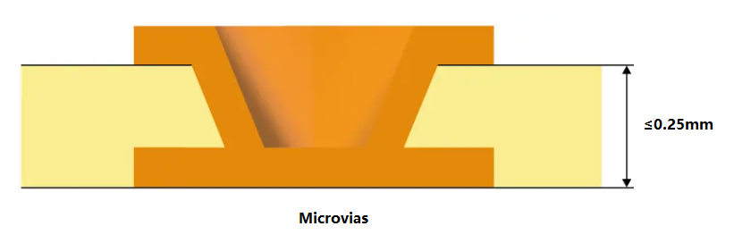
A microvia is a small hole drilled into a PCB that connects different layers. They are essential for high-density interconnections and are commonly used in advanced electronic designs. Typically, microvias equal to or less than 150 microns drilled on the PCB board with a laser. In 2013, the IPC standard changed the definition of microvias to those with an aspect ratio of 1:1. Ratio of aperture to depth (not exceeding 0.25mm). Previously, micropores were less than or equal to 0.15 mm in diameter, so they typically spanned only one layer.
Because the diameter is very small compared to mechanically drilled through holes (PTH), we define them as microvias, usually connecting only one layer of the board to its adjacent layers. These through holes reduce the possibility of any type of manufacturing defect because they are laser drilled, thus reducing the possibility of any residue remaining after the process. Because of their small size and ability to connect one layer to the next, they can make dense printed circuit boards with more complex designs.
Types of Microvias
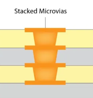
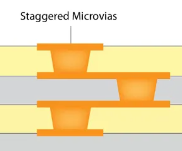
There are two types of microvias in the PCB design – stacked microvias and staggered microvias.
Stacked Microvias
Stacked microvias are formed by stacking multiple layers on top of each other to provide a path through which current flows. Create a hole in one layer and drill into another layer below. The top layer is welded or welded to the bottom layer to form an interconnect between the two layers. This allows for fast, efficient routing without compromising performance or reliability.
Staggered Microvias
The interlaced microvias is aligned with the pad of the same layer, but is offset from its center by half of the pad diameter. The distance from its center to the edge of the board is also half the diameter of the pad. Staggered microvias allow you to place two through holes in a single pad without overlapping them or having to route wires on different layers together in this location. This type of microvias can be used for electrical connections to the surrounding brass pads and traces.
What is the Difference Between Vias and Microvias?
Vias and microvias serve similar purposes in connecting different layers of a PCB, but they differ significantly in size and application.
1. Size
One of the most significant differences between vias and microvias is their size. Standard vias typically have a diameter greater than 150 micrometers (μm), while microvias are defined as having a diameter of 150 μm or less.
2. Design Complexity
As technology advances, the demand for higher circuit densities and more complex designs has grown. Microvias enable designers to create intricate multilayer circuits that were not possible with standard vias.
3. Layer Connection
Standard vias can connect any number of layers in a PCB, typically running from the outer layer through to the inner layers. In contrast, microvias are usually used for connecting one or two layers. Microvias are commonly employed in multilayer PCBs, where they can connect the outer layer to one or more inner layers without passing through the entire board.
4. Aspect Ratio
The aspect ratio, which is the ratio of the depth of a via to its diameter, is another important difference. Standard vias generally have lower aspect ratios, making them easier to fabricate. Microvias, due to their smaller size, often have higher aspect ratios. A typical aspect ratio for microvias ranges from 1:1 to 2:1.
5. Applications
Standard vias are commonly used in traditional PCB designs for applications where space is not as critical. They are suitable for general-purpose circuits, power distribution, and less complex layouts. In contrast, microvias are essential in high-density applications, such as smartphones, tablets, and advanced computing devices, where compact designs are necessary.
Microvias vs. Blind Via
Blind vias connect the outer layer of the PCB to one or more inner layers without penetrating the entire board. As the name suggests, these through-holes are “blind holes” because they are not visible from the other side of the PCB. Blind holes have several advantages, such as saving space on the board, enabling a more compact design, and improving signal integrity by reducing the length of the signal path.
The blind via passes through the surface layer of the PCB, extending through only a portion of the board to connect the surface layer to one or more inner layers. They are a key component in current PCB designs, allowing surface components to connect to inner layers while minimizing the number of layers required for wiring. The advantages of using blind vias including:
Increased density
Reduce the number of layers
Improved signal performance
Good for heat dissipation
Improve mechanical strength
Can Microvias be Designed in Multilayer MCPCB?
Yes, microvias can indeed be designed in multilayer MCPCBs. In fact, their small size and efficient design make them ideal for these types of boards. Multilayer MCPCBs often require compact interconnections to accommodate various functionalities, and microvias facilitate this need. By enabling multiple layers to connect efficiently, microvias enhance the overall performance of the MCPCB. Additionally, they contribute to improved thermal management, a critical factor in high-power applications. Their integration in multilayer designs is a significant advantage for modern electronics.
The process for using microvias in multilayer metal-based circuit boards includes the following key steps:
1. Inner laser drilling and plating: This is the first step in the production of microvias, precisely drilled by laser technology, and electroplated.
2. Resin filled: The micro-vias after electroplating are filled with resin to enhance the stability of the structure.
3. Resin grinding: Grind the orifice after the jack hole to ensure a smooth surface.
4. Electroplating: Metallize the surface of the orifice resin to achieve electrical interconnection between layers.
5. Inner circuit etching and outer layer lamination: To complete the production of the inner circuit, and the outer layer of laser drilling and graphic plating, and finally realize the production of multi-layer circuit board.
MCPCB Material in EBest Circuit (Best Technology)
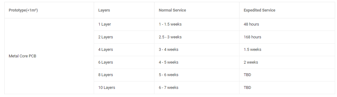
MCPCB Prototype Lead Time (Vary Depends on the MCPCB Design)
Designing and developing printed circuit boards (PCBs) may sound complex, but it’s an exciting process that is within reach, even for beginners. With the right approach, software tools, and an understanding of the basic principles, you can create functional and efficient PCBs.
Is PCB Design Difficult?
The difficulty of PCB design depends on the learning objectives and depth. If it is just the initial stage, do some simple circuit board design, then it is relatively easy. But if you want to go deep and get to expert level, in areas as diverse as pcb layout, signal integrity, electromagnetic compatibility, impedance design, and more, then you need to put in more work.
For beginners, choosing the right software and learning resources is very important. PADS from Protel, Altium Designer (AD) and Mentor Graphics are commonly used PCB design software. Protel software is simple and easy to learn, suitable for beginners to use; AD and PADS are powerful, but the operation is complex, suitable for the design of complex circuit boards.
What is the Basic Rule of PCB Design?
The key to good PCB design is layout organization. Keep the design simple, especially at the beginning. Here are a few basic rules to follow:
Control Trace Length
Controlling the length of traces means adhering to the rule of keeping traces as short as possible in PCB design to avoid unnecessary interference caused by long traces. This is especially crucial for important signal lines, such as clock signal traces, which should be placed very close to the oscillator. When driving multiple devices, the network should be determined based on specific circumstances.
Avoid Forming Self-Inductive Loops
In PCB design, it is important to pay attention to signal lines forming self-inductive loops between different layers, particularly in multilayer boards. The chances of forming self-inductive loops increase when routing signal lines between layers, and these loops can cause radiated interference.
Minimize Ground Loop Principle
The principle of minimizing ground loops is to keep the signal lines and their loops as small as possible. The smaller the loop area, the less external radiation and interference it experiences. When defining ground planes, consider the distribution of the ground plane and important signal lines to prevent issues caused by ground plane cuts.
In double-layer board designs, while leaving sufficient space for the power supply, the remaining areas should be filled with reference ground and include some necessary vias to effectively connect signals on both sides. Ground isolation should be used for key signals. For designs with higher frequencies, special attention should be paid to the signal loop problems of the ground plane, and multilayer boards are recommended.
High-Speed Signal Shielding Design
The relevant ground loop rules are also aimed at minimizing signal loop areas and are mainly used for important signals such as clock and synchronous signals. For particularly important and high-frequency signals, consider using a shielded structure design with copper coaxial cables. This means isolating the line from the ground on all sides while effectively grounding the shield layer and ensuring its connection with the ground plane.
Avoid the “Antenna Effect”
Generally, routing with one end suspended is not allowed to avoid the “antenna effect,” which reduces unnecessary interference radiation and reception; otherwise, it may lead to unpredictable results.
Chamfer Rule
PCB design should avoid sharp corners and right angles to prevent unnecessary radiation and poor manufacturing performance. The angle between all traces should be ≥135°.
Avoid Overlapping Different Power Layers
Different power layers should be spatially separated to reduce interference between them, especially between power supplies with significant voltage differences. Issues arising from overlapping power planes must be avoided, and if unavoidable, consider using an isolated ground layer.
Avoid Via Proximity to SMT Pads
If vias are not covered with a solder plug, they can easily be placed too close to SMT pads during layout. This can cause solder to flow through the via to the other side of the PCB during reflow, resulting in insufficient solder on the SMT pads and causing issues like cold solder joints. It is generally recommended to maintain a distance of more than 25 mils from the edge of the via to the SMT pad and to apply solder mask over the via.
Do Not Route Traces Wider than SMT Pads Directly into the Pads
If traces are wider than the pads, the window area of the SMT pads generally expands beyond the pad size. This means that if the solder paste on the pad is slightly insufficient during reflow, there is a risk of cold solder joints. Using traces that are slightly larger or slightly smaller than the pads can also help avoid excessive heat dissipation during soldering.
Do Not Place Components Too Close to the Board Edge
During the assembly and soldering stages of the PCB, the board will be transported through various processing areas, such as solder paste application and pick-and-place machines, followed by reflow soldering. Therefore, when designing the PCB, at least one side must leave enough space for a processing margin of at least 3 mm in width and 50 mm in length. There should be no interference between components and leads within the processing margin, as this could affect the normal transport of the PCB.
If the layout cannot accommodate this, consider adding an independent 3 mm processing margin or panel. (Note: SMT components cannot be placed within 5 mm of the edge on either side of the processing panel to facilitate reflow soldering.) If the components on your PCB are hand-soldered, you can disregard this requirement.
Keep Solder Mask Window Sizes Consistent
The solder mask layer needs openings for the pads. These openings prevent the solder mask from covering the pad area, protecting the PCB circuit from oxidation and short circuits during soldering. Typically, a solder mask layer covers the outer layers of the PCB. Common solder masks are green (though black, red, yellow, and blue are also used).
Solder should not be applied to pads to avoid solder paste sticking. To avoid the solder mask layer interfering with pad solderability due to process tolerances, it is common to design a solder mask opening that is larger than the pad by approximately 0.1 mm (4 mil). However, it is also acceptable to keep the solder mask opening area the same size as the pad dimensions; the factory will process it uniformly for you.
Reduce EMI Interference
Every PCB can be affected by EMI or become a source of interference. As part of the engineering design, special attention is required during PCB layout:
Increase the spacing between high-frequency traces and low-frequency or analog traces.
Minimize the return path for high-speed signals and ensure they do not cross split planes. Smaller current loops reduce EMI radiation intensity.
High-speed differential signals should be routed in parallel and have equal lengths; otherwise, they will offset the noise suppression characteristics of the differential pair.
Avoid using vias on high-speed traces, as they may lead to EMI emissions.
What Files Are Needed to Manufacture a PCB?
When you’re ready to manufacture your PCB, you will need to generate specific files for the fabrication process. The most common file format used by PCB manufacturers is the Gerber file. Here are some other important files that needed to submitted to manufacturer:
1. Gerber Files – your design files, include the design layout, detailing copper layers, solder masks, and silkscreen layers.
2. Drill Files – specify the locations and sizes of holes for vias and component leads.
3. Bill of Materials (BOM) – a list of all components required for the board, including part numbers and quantities.
4. Pick and Place File – guides the automated machines on where to place each component on the PCB.
What Software to Use for PCB Design?
Choosing the right software can make the design process much easier, especially for beginners. Here are a few commonly used PCB design tools:
KiCad: This is a free, open-source software that’s great for both beginners and professionals. It has a user-friendly interface and includes a schematic editor, PCB layout, and 3D viewer.
Eagle: Popular among hobbyists, Eagle offers a simple design process and an extensive component library. It’s free for small designs but has premium features for more advanced projects.
Altium Designer: For more complex projects, Altium Designer is an industry-standard tool with advanced features. While it’s pricier, it offers professional-grade tools for high-level PCB design.
How Do You Manufacture a PCB Board?
Manufacturing a PCB involves several steps, and understanding the process helps ensure your design is ready for production. Here’s a simplified overview:
Step 1: Designing the PCB
Using PCB design software to create the PCB layout. The design process includes defining the schematic, component placement, and trace routing. Designers must consider factors such as signal integrity, power distribution, and thermal management.
Step 2: Design Review and Engineering Questions
Once the initial design is complete, a thorough review is conducted. This includes checking for design rule violations, verifying component footprints, and ensuring all connections are correct. Engineers may raise questions about potential performance issues, manufacturability, and compliance with regulatory standards. Feedback from this review may lead to modifications to optimize the design.
Step 3: Printing the PCB Design
After finalizing the design, the PCB layout is printed onto a transparent film, which will be used as a photomask for the etching process. This film represents the layers of the PCB, including copper and solder mask layers.
Step 4: Printing the Copper for the Interior Layer
The copper layers are printed onto the laminate using a photoresist process. The photoresist is applied to the copper-clad laminate, and the printed film is exposed to UV light. The areas that are exposed to light will become soluble and can be washed away, leaving behind a copper pattern that matches the PCB design.
Step 5: Etch the Inner Layers or Core to Remove Copper
The exposed copper is etched away using a chemical process, leaving only the desired copper traces. This step must be carefully controlled to ensure the traces are of the correct width and spacing, as specified in the design. The etching process can be done using either chemical etching or laser etching.
Step 6: Layer Alignment
Once the inner layers are etched, they must be aligned correctly for lamination.
Step 7: Automated Optical Inspection (AOI)
Automated Optical Inspection is performed to check the accuracy of the printed copper layers. Any discrepancies, such as missing or misaligned traces, can be identified and corrected before proceeding to the next steps.
Step 8: Laminating the PCB Layers
The aligned layers are then laminated together using heat and pressure. It combines the different layers, including copper, dielectric, and solder mask layers, into a single, solid structure.
Step 9: Drilling
Once the layers are laminated, holes are drilled for vias and mounting holes. The drilling process requires precision, as these holes must align perfectly with the design specifications. Computer-controlled drilling machines are typically used to achieve the necessary accuracy.
Step 10: PCB Plating
After drilling, the PCB goes through an electroplating process where a conductive layer is added to the walls of the drilled holes.
Step 11: Outer Layer Imaging
Similar to the inner layers, the outer layers are prepared for imaging. A photoresist is applied, and the printed film of the outer layer design is aligned and exposed to UV light. The unwanted areas are washed away, leaving a pattern on the copper layer.
Step 12: Outer Layer Etching
The outer copper layers are then etched to remove the unprotected copper, leaving behind the desired copper traces.
Step 13: Outer Layer AOI
Another round of Automated Optical Inspection is conducted on the outer layers to ensure that the copper traces and pads are correctly formed.
Step 14: Solder Mask Application
A solder mask layer is applied to protect the PCB and prevent solder from bridging between components during assembly. The solder mask is typically a green epoxy coating, but it can also be available in other colors. The areas where solder is needed are left exposed.
Step 15: Silkscreen Application
Silkscreen printing is used to apply labels, component designators, logos, and other markings onto the PCB surface.
Step 16: Finishing the PCB
The finishing process includes applying surface finishes such as HASL (Hot Air Solder Leveling), ENIG (Electroless Nickel Immersion Gold), or OSP (Organic Solderability Preservative) and so many surface treatments.
Step 17: Electrical Reliability Test (E-test)
Before packaging, the PCBs undergo electrical testing to ensure that all circuits function correctly. This may include continuity testing, insulation resistance testing, and high-voltage testing.
Step 18: Profiling and Route Out
The final PCB is profiled and routed to its specific shape, including cutting out the edges and any slots or cutouts required.
Step 19: Quality Check and Visual Inspection
A final quality check and visual inspection are performed to ensure that all specifications have been met. Examining for any physical defects, such as scratches, solder mask misalignment, or improper solder application.
Step 20: Packaging and Delivery
Once all checks are complete, the PCBs are cleaned, packaged, and prepared for delivery. Proper packaging is essential to protect the PCBs during shipping.
What Is the Cheapest PCB Finish?
The cheapest finish is HASL, which is also widely used. HASL applies a thin layer of molten solder to the surface, providing good protection and easy solderability. However, it’s not always suitable for fine-pitch components or designs requiring a flat surface. Other options, such as ENIG (Electroless Nickel Immersion Gold), are more expensive but provide a smoother, more durable finish for advanced designs.
Developing a PCB for the first time can feel like a daunting task, but by understanding the basics and using the right tools, it’s a process that anyone can learn. From following simple design rules to choosing affordable software and finishes, creating a PCB can be a good experience. Working closely with manufacturers and learning through trial and error will sharpen your skills over time.
How Much Does It Cost to Get a PCB Board Made?
The cost of producing a PCB depends on several factors, such as the size, number of layers, material used, and whether you’re doing a prototype run or full production. For a simple, single-sided board, costs can start as low as $10 to $20 per board, but more complex, multi-layer designs can cost upwards of $100 or more per board.
Additional costs may include shipping, testing, and assembly if you are having components mounted by the manufacturer. It’s always a good idea to get quotes from multiple manufacturers and consider both cost and quality.
If you don’t want to develop a PCB board by yourself, choosing a reliable EMS PCB manufacturer like EBest Circuit (Best Technology). We are engaging in PCB manufacturing over 18 years, we deeply understand every design rules and know which one is best for manufacturing. Best Team offer full turnkey PCB & PCBA service for over the world. We can help to PCB design, PCB layout, PCB manufacturing, components sourcing, PCB assembly, box building, and function testing. Give us your ideal, we can make it come true!
In the electronic manufacturing process, it is usually necessary to divide a large area of aluminum-based PCB into multiple small pieces so that they can be installed in different electronic devices. Different electronic devices have different requirements for the size of PCBs. Through depaneling, large-area aluminum-based PCBs can be cut into sizes suitable for specific electronic devices.
What is the meaning of depaneling?
Aluminum PCB depaneling refers to cutting multiple circuit boards arranged in a row from a large board into separate small boards. This process is to divide a large aluminum printed circuit board (PCB) into multiple independent and fully functional circuit boards for subsequent assembly and use.
Aluminum PCB depaneling is an important link in the production process of electronic devices, which can improve production efficiency and circuit board flexibility.
What are the methods of PCB depaneling?
There are many ways to depanel aluminum PCBs. Common depaneling methods include:
1. V-cut depaneling: Use a V-shaped blade to cut a V-shaped groove on the PCB board, and then separate the aluminum PCB along the groove by external force. This method is suitable for smaller aluminum PCB boards and fine dividing lines.
2. Sawtooth depaneling: Cut the aluminum PCB board with a sawtooth cutting tool to form multiple small panels, and then separate the panels by pressure or vibration. This method is suitable for aluminum PCB boards with larger areas.
3. Laser depaneling: Use a high-energy-density laser beam to accurately cut the aluminum PCB, which is suitable for production environments with high precision requirements and high efficiency.
4. Chemical corrosion depaneling: Corrode the aluminum PCB with a chemical corrosive agent to form a dividing line, and then separate the panels by physical methods.
What is the process of depaneling PCB?
The aluminum PCB depaneling process varies depending on the depaneling method. The common aluminum PCB depaneling methods and processes are as follows:
Manual depaneling
Preparation: Check whether the aluminum PCB board meets the conditions for manual depaneling, such as confirming that there are no stress-sensitive components such as SMD (Surface Mounted Devices) on the board, and prepare suitable fixtures and operating space.
Positioning and fixing: Place the aluminum PCB concatenated or assembled boards that need to be separated on a stable workbench and fix them with fixtures to ensure that the boards do not move during the separation process. For aluminum PCB boards with V-grooves, align the V-grooves with the direction that is convenient for force application, and ensure that the board is placed in the correct direction and position to facilitate the separation operation.
Separation operation: The operator uses both hands or simple tools (such as tweezers, etc., and small cutting tools may be used in some special cases, but they must be operated with caution to avoid damaging the board) along the V-groove to break or separate the aluminum PCB board into individual small boards with appropriate force. During the operation, pay attention to controlling the force and direction to avoid damage to the board due to uneven force or wrong direction.
V-cut board separation machine separation
Equipment debugging: Turn on the power of the V-cut board separation machine, and adjust the upper guide knife position and lower knife height of the board separation machine according to the thickness of the aluminum PCB board, the depth and width of the V-groove and other parameters to ensure that the spacing between the upper and lower knives is appropriate and the aluminum PCB board can be accurately cut.
Upper board positioning: carefully place the aluminum PCB board with V groove on the workbench of the V-cut board splitter, ensure that the V groove of the aluminum PCB board fits tightly with the lower knife of the board splitter, and the position of the board is accurate to avoid deviation during the cutting process.
Board splitting operation: start the V-cut board splitter manually, electrically or pneumatically, so that the blade cuts along the V groove of the aluminum PCB board. During the cutting process, pay attention to the cutting situation to ensure that the cutting depth is moderate and will not cause over-cutting or incomplete cutting of the aluminum PCB board.
What is the manufacturing process of aluminum PCB?
The manufacturing process of aluminum substrate PCB mainly includes the following steps: cutting, drilling, dry and wet film imaging, etching, surface treatment and final inspection.
1. Cutting: Cut the large-sized incoming materials into the size required for production, pay attention to the protection of the aluminum and copper surfaces, and avoid scratches and board edge delamination.
2. Drilling: Position the holes in the board to ensure the correct number and size, and avoid scratches on the board and deviation of the hole position.
3. Wet and dry film imaging: Present the parts required for making the circuit on the board, and pay attention to whether the circuit is open and whether the alignment is deviated after development.
4. Etching: Remove the uncovered parts to form the circuit pattern, and pay attention to the quality and stability of the circuit after etching.
5. Surface treatment: Perform necessary surface treatment on the circuit board, such as tin spraying, to improve the performance and appearance of the circuit board.
6. Final inspection: Perform a final inspection on the completed circuit board to ensure that the quality meets the requirements.
What are the advantages of aluminum PCB?
The main advantages of aluminum substrate PCB include:
Excellent heat dissipation performance: The aluminum substrate uses high thermal conductivity aluminum alloy as the core material, which can quickly conduct and dissipate heat, thereby effectively reducing the operating temperature of components.
Lightweight design: Compared with traditional FR4 substrates, aluminum substrates have lighter weight, which is particularly important in weight-sensitive fields such as aerospace and automobiles, helping to reduce the weight of the overall equipment and improve energy efficiency and operating performance.
Good mechanical properties: Aluminum substrates have high strength and hardness, providing good support and protection for electronic components. At the same time, its excellent impact resistance and vibration resistance enable it to adapt to various complex working environments and ensure the stable operation of the equipment.
Excellent electrical performance: Aluminum substrates have excellent insulation and voltage resistance, which can meet the electrical requirements of electronic equipment in various working environments and provide stable electrical support for the equipment.
Environmental protection: Aluminum substrates are made of environmentally friendly materials, there is no pollution in the production process, and waste is easy to recycle and dispose, which is fully in line with the current trend of green environmental protection.
Diverse application forms: There are many types of aluminum substrates, including flexible aluminum substrates, hybrid aluminum substrates, multi-layer aluminum substrates, etc., suitable for different application needs.
What are the disadvantages of aluminum PCB?
The main disadvantages of aluminum PCB include high cost, difficult process, electrical strength and withstand voltage problems, mismatched thermal conductivity test, inconsistent material specifications, and more defective products.
First, the price of aluminum PCB is relatively high, usually accounting for more than 30% of the product price. This is because the production of aluminum PCB requires the use of high-purity aluminum materials and special processing technology, all of which push up the cost.
Second, the process of aluminum PCB is difficult, especially when it is made into a double-sided board, the process complexity is higher, and it is easy to have problems in electrical strength and withstand voltage. In addition, the mismatch of thermal conductivity test methods and results of aluminum PCB is also a problem.
In addition, the material specifications of aluminum PCB have not yet been unified, and there are multiple standards such as CPCA industry standards, national standards, and international standards, which brings certain uncertainties to production and application.
Why is aluminum no longer used in integrated circuits?
The main reason why aluminum is no longer used in integrated circuits is that copper has replaced aluminum as an interconnect metal material. Copper has lower resistivity and better anti-electromigration performance than aluminum, which makes copper more reliable and effective in high-speed integrated circuits.
Specifically, aluminum may experience electromigration under long-term current, that is, aluminum atoms migrate inside the wire, causing the wire to break or form voids, which in turn causes the integrated circuit to fail. In addition, as the interconnection spacing decreases, the resistance of the aluminum wire increases and the capacitance between the wires increases, resulting in increased RC delay, which is not conducive to high-speed integrated circuits.
Copper has a lower resistivity than aluminum, can transmit current more efficiently, and can carry more current in thinner metal wires. Copper also has higher electromigration resistance than aluminum, making copper interconnects more reliable under high current conditions. These advantages make copper a preferred material for advanced integrated circuit technology.
Aluminum-based PCB depaneling is an important link in the electronic manufacturing process, which directly affects the quality and performance of electronic equipment. By selecting the appropriate depaneling method, controlling the depaneling accuracy, and avoiding damage to the PCB, the quality and efficiency of aluminum-based PCB depaneling can be effectively improved.
There are many differences between single sided and double sided PCB in terms of structure, performance, application scenarios, etc. Single-sided PCB has conductive lines on only one side, while double-sided PCB has conductive lines on both sides, which makes them perform differently in terms of the complexity of circuit layout, signal transmission capability, and the types of electronic devices they are suitable for.
What is the difference between single and double sided PCB?
The main difference between single-sided PCB and double-sided PCB lies in their structure and use. Single-sided PCB has only one layer of lines, which is suitable for simple circuits; while double-sided PCB has two layers of lines, which is suitable for complex circuits.
The characteristics and application scope of single-sided PCB are as follows:
1. Structure: Single-sided PCB has only one layer of lines, and all components are on the same layer and connected by copper foil lines.
2. Application scope: Usually used for simple circuits, such as LED lights, alarm clocks, etc.
3. Advantages: Low manufacturing cost and simple manufacturing process.
4. Disadvantages: Only simple circuit layout can be realized, and the crossing of lines will increase the size of the board, which is not suitable for complex circuit layout.
The characteristics and application scope of double-sided PCB are as follows:
1. Structure: Double-sided PCB has two layers of lines, and components can be arranged and connected on two levels, and connected to each other through jacks and pads.
2. Application scope: Usually used for complex circuits, such as computers, mobile phones, etc.
3. Advantages: Complex circuit layout can be realized, and the crossing of lines will reduce the size of the board.
4. Disadvantages: The manufacturing cost is high, and the manufacturing process is more complicated than that of single-sided PCB, which is not suitable for ultra-large circuit layout.
The differences in materials and processes between single-sided PCB and double-sided PCB are as follows:
1. Material: Single-sided board has copper foil on only one side, while double-sided board has copper foil on both sides.
2. Process: The solder joints of single-sided board are basically on one side, and components are inserted on the other side; both sides of double-sided board can be soldered, with plug-in components and SMD components.
Why use single sided PCB?
Single-sided PCB is mainly used for simple circuit design and cost-sensitive applications. Since there is only one side of the single-sided board with wiring, the wiring is difficult, so it is mainly suitable for simple circuit design.
The advantages of single-sided PCB include low cost and relatively simple manufacturing process. Since the manufacturing process of single-sided board is relatively simple and does not require complex multi-layer wiring and connection, the cost is low and suitable for mass production.
What is the advantage of single layer PCB?
The main advantages of single-layer PCB include:
1. Low cost: The manufacturing cost of single-layer PCB board is relatively low, because only one layer of copper foil and one layer of substrate are required, the manufacturing process is relatively simple, and the material cost is low.
2. Easy to make: Compared with other structural types of PCB boards, the manufacturing method of single-layer PCB board is relatively simple, only single-sided wiring and single-layer corrosion are required, the manufacturing difficulty is low, the drilling, welding and installation of components are relatively simple, and it is unlikely to cause production problems.
3. High reliability: Single-layer PCB board does not have multi-layer wiring and connection, so it is not easy to have problems such as short circuit and interference, and has high reliability.
4. Suitable for simple circuits: Single-layer PCBs are suitable for simple circuit designs, such as LED lights, household appliances, etc., and can meet most low-complexity circuit requirements.
What are the disadvantages of single sided PCB?
First, the difficulty of wiring a single-sided PCB is a significant disadvantage. Since there is only one layer of copper foil, wiring is difficult, and the layout of the circuit and the location of components need to be carefully planned to avoid short circuits or circuit failures caused by improper wiring.
Second, the electromagnetic interference suppression capability of single-sided PCBs is relatively poor. In high-frequency circuits, the electromagnetic interference problem of single-sided PCBs will be more prominent and become an important factor to be considered during design.
Finally, single-sided PCBs limit the complexity of the circuit. Since it has only one layer of copper, it is not suitable for the design of complex circuits. For circuits that require high complexity, double-sided or multi-layer PCBs would be a better choice.
1. Enhanced circuit density: The available surface area of double-sided PCBs is doubled, and more components can be attached.
2. Higher signal transmission rate: Double-sided PCB design makes the circuit more complex and flexible, thereby improving the signal transmission rate and circuit performance.
3. More reliable circuit connection: By passing the circuit through holes between the two sides, the circuit can be connected on both sides, greatly improving the density and reliability of the circuit board.
4. Convenient wiring and debugging: The design of double-sided PCB makes wiring more flexible, convenient for complex circuit design, and also convenient for subsequent debugging and maintenance.
5. Environmental protection and high efficiency: Double-sided PCBs are made of non-toxic and pollution-free materials, which meet environmental protection requirements, and can carry more electronic components and improve the working efficiency of equipment.
Where are double sided PCBs used?
The characteristic of double-sided PCBs is that both sides can be wired and assembled with electronic components, and the lines on both sides are connected through holes (vias), so as to achieve more complex circuit design.
This design makes double-sided PCBs perform well in application scenarios that require high-density assembly and complex circuit layout. Due to the presence of vias, double-sided PCBs can achieve more complex circuit designs without significantly increasing the size of the circuit board.
Specific application areas include:
1. Computer and industrial control: Double-sided PCBs are widely used in computer motherboards and industrial control systems, providing complex circuit designs and high-density component layouts.
2. Communication equipment: In communication equipment, double-sided PCBs are used to achieve high-density signal processing and transmission, supporting various communication protocols.
3. Consumer electronics: In devices such as smartphones, tablets, routers, etc., double-sided PCBs are used to achieve complex circuit functions and efficient space utilization.
4. Aerospace: In the high-tech field, double-sided PCBs are used for applications with high performance requirements and strict space constraints.
What are the two sides of a PCB called?
The two sides of a PCB are called the top layer and the bottom layer.
The top layer is usually used to place and layout electronic components such as chips, resistors, capacitors, etc. The pins, wires, identifiers, and markings of the components can be seen on this layer. The top layer is also called the component side.
The bottom layer is mainly used to connect the pins of electronic components and connect to the top layer through appropriate wires. In this layer, you can see the pads, vias, connections, and possible ground and power planes. The bottom layer is also called the solder side.
In addition to the top and bottom layers, PCBs may also contain other layers, such as signal layers, power/ground layers, mechanical layers, solder mask layers, solder paste protection layers, and no-routing layers. These layers play different roles in PCB design, such as providing circuit routing, mechanical support, and preventing short circuits.
Can you put components on both sides of a PCB?
Components can be placed on both sides of a PCB. The design of double-sided PCBs allows components and wiring to be placed on both sides of the circuit board, thereby increasing the complexity and functionality of the circuit.
Design features of double-sided PCBs include:
Dual use of wiring and components: Both sides of a double-sided PCB can be used for wiring and component placement, which greatly increases the complexity and functionality of the circuit.
Via connection: In order to achieve interconnection between components and wiring on a double-sided PCB, connections need to be made through vias. A via is a small hole filled or coated with metal that connects wires on both sides.
The use scenarios of double-sided PCBs include:
Increasing circuit density and functionality: Double-sided PCBs increase the layout space for components, allowing designers to achieve more functions without increasing the size of the circuit board, which is particularly suitable for occasions that require high-density integration and complex circuit design.
In short, single-sided and double-sided PCBs differ significantly in many aspects. Both single-sided and double-sided PCBs contribute to the vigorous development of the electronics industry and continue to help electronic technology move forward. BEST Technology has abundant upstream and downstream resources for circuit boards, and can quickly and efficiently meet customers’ various needs for circuit boards.
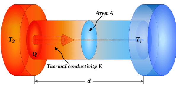
Thermal conductivity refers to a material’s ability to conduct heat. It’s a physical property that indicates how easily heat can pass through a substance when there is a temperature difference. In scientific terms, thermal conductivity is measured in watts per meter-kelvin (W/m·K), describing how much heat (in watts) is transferred through a material for every meter of thickness when there’s a one-degree temperature difference across it.
For ceramic materials, thermal conductivity plays a pivotal role in determining their usability in various industrial and electronic applications. Materials with high thermal conductivity can transfer heat quickly, so it is important in situations where heat must be dissipated rapidly to avoid damage to components, like in electronics or aerospace industries. On the other hand, materials with low thermal conductivity are used for thermal insulation, preventing unwanted heat transfer in applications like kiln linings or fireproofing.
Do Ceramic Materials Have High Thermal Conductivity?
Ceramic materials are generally known for their thermal insulation properties, meaning they typically have low thermal conductivity. However, not all ceramics are insulators. There are a few exceptions with significantly higher thermal conductivity, making them valuable for heat-dissipating applications.
Traditional ceramics such as alumina and zirconia are typically poor conductors of heat due to their atomic structure, which restricts the movement of heat. However, advanced ceramics like aluminum nitride (AlN) and silicon carbide (SiC) exhibit impressive levels of thermal conductivity. These materials are increasingly being used in industries like electronics, aerospace, and automotive manufacturing, where managing heat efficiently is critical to the performance and safety of equipment.
High thermal conductivity ceramics, though less common, have opened new avenues for using ceramic materials in areas where heat transfer was traditionally a limiting factor. So, while most ceramics are not known for high thermal conductivity, advancements in ceramic technology have led to the development of high-performance materials that challenge this generalization.
Why is Thermal Conductivity Important for Ceramic Materials?
Thermal conductivity in ceramics is a key factor that dictates where and how these materials can be used. There are several reasons why thermal conductivity matters for ceramic materials:
Heat Management in Electronics
In electronics, high thermal conductivity ceramics are crucial to ensure that components do not overheat during operation. Many electronic devices produce heat as a byproduct, and if this heat is not managed properly, it can lead to equipment failures. Ceramic materials like AlN and BeO are widely used in applications such as LED packaging, power electronics, and semiconductor manufacturing due to their ability to transfer heat away from sensitive components quickly and efficiently.
Thermal Insulation
On the flip side, some ceramic materials with low thermal conductivity are perfect for insulation. In industries like metallurgy or construction, materials like silicon oxide or zirconia are used to keep heat in or out, making them excellent choices for furnace linings, kilns, and thermal barrier coatings.
Thermal Shock Resistance
Many ceramics with low thermal conductivity also possess high thermal shock resistance, meaning they can withstand rapid temperature changes without cracking or breaking. This is important in applications such as aerospace, where materials are often exposed to extreme temperature variations.
Energy Efficiency
Thermal conductivity affects the energy efficiency of systems. In applications like heating elements, components with good thermal conductivity allow heat to be transferred more effectively, leading to better energy efficiency and lower operational costs. Ceramics that balance both thermal insulation and conductivity provide optimized energy management, crucial for industrial processes.
5 Typical High Thermal Conductivity Ceramic Materials
Aluminum Nitride (AlN)
Thermal Conductivity: ~170-230 W/m·K
Aluminum nitride is one of the most well-known ceramics for high thermal conductivity. It is electrically insulating, which makes it an ideal material for electronic substrates and heat sinks in devices like LEDs and power modules. Its ability to rapidly dissipate heat while maintaining electrical isolation makes it a popular choice in electronics where heat management is critical.
Silicon Carbide (SiC)
Thermal Conductivity: ~120-270 W/m·K
Silicon carbide is not only known for its excellent thermal conductivity but also its incredible hardness and mechanical strength. It is used in high-temperature applications, such as in gas turbines and heat exchangers. Its ability to withstand harsh conditions while transferring heat efficiently makes it invaluable in aerospace and automotive industries.
Beryllium Oxide (BeO)
Thermal Conductivity: ~200-330 W/m·K
Beryllium oxide offers one of the highest thermal conductivities among ceramics, rivaling some metals. Its superior ability to conduct heat while remaining electrically insulating makes it ideal for high-performance electronic devices. However, its use is limited due to the toxic nature of beryllium, requiring careful handling during manufacturing.
Alumina (Al2O3)
Thermal Conductivity: ~20-35 W/m·K
Alumina is a widely used ceramic due to its good combination of thermal conductivity, mechanical strength, and electrical insulation. Though not as high in thermal conductivity as AlN or SiC, alumina’s affordability and versatility make it a common choice in many industrial applications, including substrates for electronics and thermal barriers.
Silicon Nitride (Si3N4)
Thermal Conductivity: ~20-30 W/m·K
Silicon nitride is a material prized for its thermal shock resistance and mechanical strength. Though it does not have the highest thermal conductivity, its ability to withstand extreme temperatures and thermal cycling makes it valuable in engines and high-performance bearings.
What Ceramic Materials Are Best for Thermal Conductivity?
Aluminum nitride is one of the most suitable ceramic materials for conducting heat. aluminum nitride (AlN) has a thermal conductivity of 170-230 W/mK, is one of the best thermal conductivity ceramic substrate materials, especially suitable for high power density and high-frequency electronic devices heat. Aluminum nitride is suitable for heat conduction, mainly for the following reasons:
1. High thermal conductivity: aluminum nitride has extremely high thermal conductivity and can effectively transfer heat from one area to another.
2. Excellent mechanical properties: aluminum nitride not only has good thermal conductivity, but also has high mechanical strength and chemical stability, can maintain the stability of its structure and properties in a variety of environments.
3. Wide application: aluminum nitride is widely used in the heat dissipation of high power density electronic devices and high-frequency electronic devices to meet the needs of modern electronic equipment for efficient heat dissipation.
What are the Thermal Properties of Ceramic Materials?
The thermal properties of ceramic materials mainly include melting point, heat capacity, thermal expansion and thermal conductivity. The melting point of ceramic materials is generally higher than that of metals, up to 3000℃ or more, and has excellent chemical stability at high temperatures.
The heat capacity of ceramic materials refers to the heat required to increase the temperature of ceramic materials by 1℃ per unit mass. Ceramic has a lower heat capacity, which means that it is less able to absorb heat when heated.
The coefficient of thermal expansion of ceramic materials is small, much lower than that of metal. This means that when the temperature changes, the size of the ceramic changes less and has good dimensional stability.
The thermal conductivity of ceramic materials is lower than that of metal materials, but its thermal conductivity depends on the specific type of ceramic. Some ceramics are good thermal insulation materials, while some ceramics are good thermal conductivity materials, such as boron nitride and silicon carbide ceramics.
Your Most Reliable Ceramic PCB Manufacturer – EBest Circuit (Best Technology)
When it comes to finding a reliable manufacturer for ceramic PCBs, EBest Circuit (Best Technology) stands out in the market. As a leader of ceramic material and ceramic PCB manufacturer, EBest Circuit (Best Technology) has over 18 years experience, we are so confident that we can provide the highest quality and high specification PCB for you! Backing up with a group of professional engineers, and well established quality system. EBest Circuit (Best Technology) has grown to become a major PCB manufacturer in Asia to serve in diverse customers base. At EBest Circuit (Best Technology), you can enjoy a full turn-key service from IC substrate design, prototyping, mass production and ceramic PCB assembly.
Whether you need ceramic materials with high thermal conductivity for your electronics, or specialized products for unique applications, we have the expertise and the technology to deliver. Trust EBest Circuit (Best Technology) to provide you with the best in ceramic PCB manufacturing, ensuring that your projects are completed to the highest standards.
Aluminum LED PCB board are almost everywhere in our lives. LED lights have become more popular than other lights in the field of lighting. LED PCBs usually use aluminum or metal core as substrates. Aluminum can dissipate heat effectively and there is no need to use a heat sink, so the PCB can effectively dissipate a lot of heat without problems.
What is aluminum led pcb board?
Aluminum LED PCB board is a special printed circuit board that is mainly used for LED lighting and other equipment that requires efficient heat dissipation. Unlike traditional FR-4 fiberglass boards, aluminum LED PCB boards use aluminum alloy as the substrate and have better thermal conductivity. This type of board usually consists of a three-layer structure: circuit layer (copper foil layer), insulation layer, and metal base layer.
The characteristic of aluminum LED PCB board is that it uses aluminum alloy material, which has excellent thermal conductivity and can quickly dissipate the heat generated when the LED is working. Compared with traditional FR-4 fiberglass boards, aluminum substrates have higher thermal conductivity and can carry higher currents, which are suitable for applications that require high power output.
In addition, aluminum substrates also have good electrical insulation and machining properties, which makes them also have a place in high-end applications.
In terms of application, aluminum LED PCB boards are mainly used in products such as LED lighting equipment and solar street lights that require efficient heat dissipation. Due to its excellent thermal conductivity and cost-effectiveness, aluminum substrates have quickly become the preferred material in these fields.
Why choose aluminum led pcb board?
The main reason for choosing aluminum-based PCB boards is that they are due to their excellent thermal conductivity and light and high-strength characteristics, which can effectively reduce the operating temperature of LED lights and improve their stability and reliability.
The advantages of aluminum-based PCB boards include:
Excellent thermal conductivity : The aluminum substrate uses metal aluminum as the substrate, which has excellent thermal conductivity, can effectively conduct the heat generated by the LED when it is working, reduce the module operating temperature, extend the service life, and improve the power density and reliability.
Lightweight and high strength : The aluminum substrate material is light and has high strength, which is suitable for various complex environments and high-strength application scenarios .
Electromagnetic shielding performance: Aluminum substrate has good electromagnetic shielding performance, which can effectively reduce electromagnetic interference and improve the signal transmission quality of electronic equipment.
High degree of customization: Aluminum substrate can be customized according to customer needs to meet the specific needs of different application scenarios.
Disadvantages of aluminum led pcb board
The main disadvantages of aluminum LED PCB board include high cost, difficult process, electrical strength and voltage resistance problems.
First, the cost of aluminum LED PCB board is high. Compared with other materials, the price of aluminum substrate accounts for more than 30% of the product price, which increases the cost of the product to a certain extent.
Secondly, aluminum LED PCB board has certain difficulties in process. The current mainstream products are mainly single-sided boards, and the process of making double-sided boards is more difficult.
In addition, aluminum LED PCB boards are prone to problems in electrical strength and voltage resistance. Due to the characteristics of the material itself, the manufactured products may not meet the standards in terms of electrical strength and voltage resistance.
What are the types of LED PCB boards?
LED PCB boards are printed circuit boards for mounting LEDs. Their substrate materials mainly determine the thermal conductivity of LED PCBs. According to the different heat dissipation performance, LED PCB boards can be divided into 6 types.
Aluminum LED PCB: Aluminum LED PCB is the most common and cost-effective printed circuit board for LED lights, such as LED plant growth lights.
Copper-based LED PCB: Copper-based LED PCB is used for high-power LED lights, such as car headlights. The structure of ordinary copper-based LED PCB is the same as that of aluminum LED PCB, but the thermal conductivity is several times higher than that of aluminum LED PCB.
FR-4 LED PCB: If the LED light is used as daily household lighting and does not require much printed circuit board heat dissipation, FR-4 LED PCB can be a cost-effective printed circuit board choice. The price of FR-4 LED PCB is lower than other types of circuit boards.
Ceramic LED PCB: High-power LED lights, especially photography and pool lights, use ceramic LED PCB. Ceramic LED PCBs include aluminum nitride (AlN) PCBs, aluminum oxide (alumina) PCBs, boron oxide (BeO) PCBs, and silicon nitride (Si₃N₄) PCBs. The most common ceramic LED PCBs are AlN PCBs and alumina PCBs.
Hybrid substrate LED PCBs: The substrate materials of high-power LED PCBs can be mixed. Hybrid LED PCBs can have two or three substrate materials. And the different substrate materials are connected by phase change, that is, they are combined into a whole.
Flexible LED PCBs: Flexible PCBs with polyimide or polyester substrates are used for flexible LED light strips. Flexible LED PCBs can be used for mask lights, miner headlamps, and indoor/outdoor decorative light strips.
What is a SMD LED PCB board?
SMD LED PCBs are printed circuit boards for surface mounted LEDs (Surface Mounted Devices). SMD LED PCBs are LED chips packaged into lamp beads, which are then soldered on PCBs to make LED modules with different spacings. In this packaging method, each lamp bead is an independent point light source, which has the advantages of small size, large scattering angle, good luminous uniformity and high reliability.
The characteristics of SMD LED PCB board include:
1. Principle of luminescence: When the current passes through the compound semiconductor, the electrons and holes combine to release energy and emit light, which belongs to cold luminescence, and the life span is about 50~100 times longer than that of tungsten filament bulbs, up to 100,000 hours.
2. Fast response speed: The lighting response speed is faster than that of ordinary electric lights, about 3~400 nanoseconds.
3. Energy saving and high efficiency: The electro-optical conversion efficiency is high, the power consumption is small, and it saves about 1/3~1/20 of the energy compared with the light bulb.
4. Wide application: It is mainly used in lighting systems, decorations, electronic equipment indicators, backlights, displays and instruments.
How to make aluminum led pcb board?
LED circuit boards usually have good thermal conductivity, electrical insulation, and mechanical processing performance, and are mainly composed of metal-clad copper plates, conductive layers, and insulating layers.
The main manufacturing processes of LED PCB include:
1. Raw material cutting
2. Drilling
3. Image transmission
4. Etching
5. Screen printing
6. Solder mask
7. Surface treatment
8. V-shaped cutting
9. Testing
10. FQC and packaging
What do G, R, B and + mean on the LED PCB?
On the LED PCB, G, R, B and + represent the following meanings:
G stands for ground: It is the zero potential reference point in the circuit, and the potential of all other circuits is measured relative to the ground. The ground plays the role of providing reference potential and preventing mutual interference between circuits in the circuit.
R stands for red: In LED display screens, R usually refers to red light-emitting diodes, which are used to produce red light. Red light is part of the visible spectrum and is often used in color displays or lighting systems.
B stands for blue: Also in LED display screens, B stands for blue light-emitting diodes, which are used to produce blue light. Blue light, together with red and green light, can synthesize various colors and is widely used in color display technology.
+ represents positive supply voltage: In the circuit, the + symbol usually represents the positive supply, that is, the power supply end that provides positive voltage. This is an important part of the power supply in the circuit to ensure the normal operation of electronic components.
In short, aluminum-based LED PCB boards occupy an important position in the electronics field with their excellent heat dissipation performance, reliable electrical performance and high mechanical strength. With the continuous advancement of technology, it will continue to bring more efficient solutions to many industries such as lighting, display screens, and automotive electronics.
Aluminum nitride PCB also known as Aluminum nitride ceramic PCB or short for AlN PCB. It is a high-performance circuit board made from aluminum nitride ceramic, a material known for its exceptional thermal conductivity and electrical insulation properties. These boards are commonly used in industries where efficient heat dissipation is crucial, such as in power electronics, LED applications, and high-frequency devices. AlN PCBs are gaining popularity due to their ability to withstand extreme temperatures.
Benefits of AlN PCBs
One of the key advantages of AlN PCBs is their excellent thermal conductivity, which helps prevent overheating in electronic components. With exceptional thermal conductivity of 170 W/mK, strong dielectric strength, and a low thermal expansion coefficient (CTE <4 ppm/°C), AlN is widely used in applications like high-power LEDs, lasers, high-current switches, and even ultra-low temperature vacuum electronics such as those in quantum computing. In addition to these features, AlN offers the same benefits as other ceramic materials, including rigidity, environmental and chemical resistance, and 0% water absorption.
Key reasons for choosing Aluminum Nitride over other PCB materials include:
Outstanding thermal conductivity of 170 W/mK
Excellent dielectric properties
High operating temperatures exceeding 350°C
Low thermal expansion coefficient (<4 ppm/°C)
Compact designs due to better integration
Hermetically sealed packages with 0% water absorption
Minimal to no outgassing
What is the Thermal Conductivity of Aluminum Nitride PCB?
The thermal conductivity of aluminum nitride PCB ranges from 170-230W/(m·K).
The high thermal conductivity of aluminum nitride PCB is due to its unique structure and chemical composition. The thermal conductivity of aluminum nitride ceramic substrate is 2-3 times higher than that of traditional alumina ceramics and silicon-based ceramics, and 10-20 times higher than that of titanium substrate. This high thermal conductivity allows them to effectively dissipate heat from high-power electronic components, preventing overheating and ensuring stable performance. The ability to manage heat efficiently makes AlN PCBs an ideal choice for applications that generate a significant amount of heat, such as power modules, LEDs, and RF components. In comparison to other materials like aluminum oxide, which has lower thermal conductivity (around 20-30 W/mK), aluminum nitride stands out as a top choice for heat-sensitive applications.
Factors affect thermal conductivity of AlN PCB
Although the theoretical thermal conductivity of AlN is extremely high, its performance in practical applications is limited by a number of factors, mainly including:
Microstructure
Phonon scattering is a key mechanism for heat conduction. Grain boundaries, interfaces, second phases, and defects can all affect the mean free path of phonons, thereby influencing thermal conductivity. High-purity, low-defect single-crystal AlN has a longer phonon mean free path and higher thermal conductivity.
Oxygen Impurity Content
AlN’s strong affinity with oxygen leads to the easy introduction of oxygen impurities, which form alumina films and lattice defects, such as aluminum vacancies. These significantly reduce the phonon mean free path, lowering thermal conductivity. When the oxygen concentration is below 0.75%, oxygen atoms primarily replace nitrogen atoms in the lattice; however, exceeding this concentration causes aluminum vacancies to disappear and results in the formation of extended defects, further affecting thermal conductivity.
Sintering Process and Additives
By selecting appropriate sintering additives (such as Y₂O₃-Li₂O, Y₂O₃-CaC₂ composite systems), densification can be achieved at lower temperatures, while reducing the formation of oxygen impurities and second phases, effectively improving the thermal conductivity of AlN ceramics. These additives help purify grain boundaries and optimize the microstructure, facilitating more efficient phonon transmission.
What is Aluminum Nitride PCB Used For?
Aluminum nitride as a stable hexagonal wurtzite covalent bond compound, has shown extensive application potential in the field of electronics and optoelectronics due to its unique physical and chemical properties. Its crystal structure takes AlN4 tetrahedron as the basic unit, space group P63mc, belongs to the hexagonal crystal system, which gives AlN a series of excellent properties and use in advanced applications.
Some common applications include:
Optical Communication
Integrated Circuits and High-Power Electronic Devices
Power Electronics
Wafer chips
Epoxy Resin Packaging
Optical Devices and Piezoelectric Devices
Industrial Materials
Acoustic Devices
Aerospace
Military
Why is Aluminum Nitride Expensive?
The high cost of aluminum nitride PCBs stems from several factors.
First of all, the raw material cost of aluminum nitride PCB is higher. The preparation of aluminum nitride powder requires high purity raw materials, synthesis methods include direct nitriding method, carbothermal reduction method, self-propagating high temperature synthesis and chemical vapor deposition method, etc. These methods have high requirements on equipment and technology, resulting in higher costs.
Secondly, the production process is complicated. The preparation process of aluminum nitride PCB is complex, including multiple steps such as molding and sintering, which has high requirements for equipment and technology and a high production threshold.
Finally, the market demand is large. Aluminum nitride PCB in power electronics, communication equipment, automotive electronics and other fields have a wide range of applications, especially in high power, high frequency and other occasions, its excellent heat dissipation and insulation performance can not be replaced, resulting in short supply in the market, the price of natural rising.
Aluminum Nitride PCB vs. Alumina Oxide PCB
Both aluminum nitride (AlN) and alumina oxide (Al2O3) are ceramic materials used in PCB manufacturing, but they differ significantly in terms of performance. AlN offers superior thermal conductivity, typically 170-230 W/mK, compared to aluminum oxide’s lower range of 20-30 W/mK. This makes AlN the better option for applications requiring efficient heat dissipation, such as high-power electronics and LED lighting.
However, aluminum oxide is more cost-effective and is often used in applications where high thermal conductivity is not as crucial. While Al2O3 provides good electrical insulation and is easier to produce, it may not perform as well in heat-sensitive environments as AlN. Therefore, the choice between AlN and Al2O3 depends on the specific thermal and budgetary requirements of the application. Here are the parameters of AlN and Al2O3 materials:
Parameter
Aluminum Nitride (AlN)
Alumina Oxide (Al2O3)
Thermal conductivity
170-230 W/m.k
24-30 W/m.k
Dielectric constant
8.8
9.2-10
Dielectric strength
15-25kV/mm
10-15kV/mm
Temperature resistance
1000-1500C
1000-1200C
CTE
4.0 ppm/K
6.5-7 ppm/K
Flexural strength
450MPa
320MPa
Dielectric breakdown voltage
14 V/m
10 V/m
AlN Ceramic PCB Design Considerations
When designing an aluminum nitride PCB, several factors need to be considered to optimize performance:
1. Trace Width
The trace width on AlN PCBs should be a minimum of 10 mils. This ensures that the conductor cross-section is sufficient to handle the current and heat dissipation needs. Given the thermal advantages of AlN, wider traces help in spreading heat more efficiently, minimizing the risk of overheating in power-dense applications.
2. Trace Clearance
Clearances between adjacent traces should be at least 8 to 10 mils. AlN PCBs often work with higher voltage levels, making spacing critical to prevent arcing or dielectric breakdown. In high-power designs, careful spacing between traces reduces the likelihood of signal interference and maintains the board’s insulation integrity.
3. Via Pads
For via pads, a minimum diameter of 16 mils is recommended. This provides sufficient area for stable soldering and ensures proper electrical connection through the via. Depending on the board’s application, larger via pads may be necessary to accommodate higher currents or thermal dissipation needs. Via sizing should also account for assembly techniques, such as reflow soldering or thermal management features, like thermal vias, which enhance heat transfer away from components.
4. Pad Geometry Adjustments
Unlike FR-4 designs, AlN PCBs often require specific adjustments in pad geometries. The mechanical and thermal properties of AlN are quite different from those of traditional PCBs. The expansion rate, hardness, and substrate fragility mean that pad designs should allow for thermal expansion and contraction without causing stress fractures. Proper pad design also ensures better solder joint reliability, particularly for components exposed to continuous thermal cycling.
5. Gold Plating for Wire Bonding Pads
In high-performance applications, wire bonding is often used, and gold plating is a preferred surface finish for wire bonding pads. The use of gold provides a stable, corrosion-resistant surface that improves bond integrity and longevity. Wire bonding is especially critical in high-frequency, high-reliability devices, where the connections must maintain integrity under thermal stress or in harsh environments.
6. Component and Solder Matching
All components and solder materials must match the electrical and mechanical properties of the AlN substrate. Mismatches in thermal expansion between the PCB material and components can lead to stress, causing cracking or delamination. It’s important to select components and solder that can withstand high temperatures and thermal cycles while maintaining compatibility with AlN’s characteristics, especially in applications like power electronics and RF circuits.
7. Hermetic Sealing and Height Restrictions
For applications requiring hermetic sealing, such as aerospace or medical devices, height restrictions may apply to the components on the PCB. Hermetic seals protect against moisture and environmental contaminants, ensuring long-term reliability in sensitive applications. The overall component height should be kept in line with the sealing requirements, and compact designs are often necessary to meet stringent packaging constraints.
8. Thermal Expansion Management
When attaching large dies or high-power devices, it’s crucial to model and account for thermal expansion. Even though AlN has a low thermal expansion coefficient (<4 ppm/°C), the difference in expansion rates between components and the substrate can create mechanical stress, especially during thermal cycling. Careful design, including flexible connections or underfill materials, can help mitigate these effects.
9. Thermal Vias
Thermal vias are essential for managing heat in high-power applications. By placing thermal vias directly underneath hot components, heat can be efficiently transferred away from sensitive areas, extending the lifespan of both the components and the PCB itself. In many designs, a network of thermal vias is integrated with heat sinks or spreaders to further improve heat dissipation.
10. Surface Finishes and Coatings
Aluminum nitride PCBs can benefit from surface finishes such as electroless nickel immersion gold (ENIG) or immersion silver, which protect the copper traces from oxidation and provide excellent solderability. The choice of surface finish may also depend on the specific application environment and the reliability requirements, especially in high-power or high-frequency circuits.
FAQs About AlN PCBs
1. How durable are aluminum nitride PCBs?
AlN PCBs are highly durable and can withstand extreme temperatures and harsh environments.
2. Can AlN PCBs be used in high-frequency applications?
Yes, aluminum nitride PCBs are well-suited for high-frequency and high-speed applications due to their excellent electrical insulation and low signal loss.
3. Are aluminum nitride PCBs environmentally friendly?
While the production process can be resource-intensive, AlN PCBs offer longer lifespans and higher efficiency, which can reduce the environmental impact over time.
4. How do AlN PCBs compare with metal-core PCBs?
Metal-core PCBs, such as those with an aluminum core, provide good thermal management but lack the superior electrical insulation of AlN PCBs. AlN PCBs are preferred for applications requiring both high thermal conductivity and insulation.
5. What industries typically use aluminum nitride PCBs?
Industries like power electronics, aerospace, automotive, and telecommunications commonly use AlN PCBs for their high-performance needs.