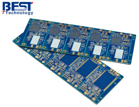
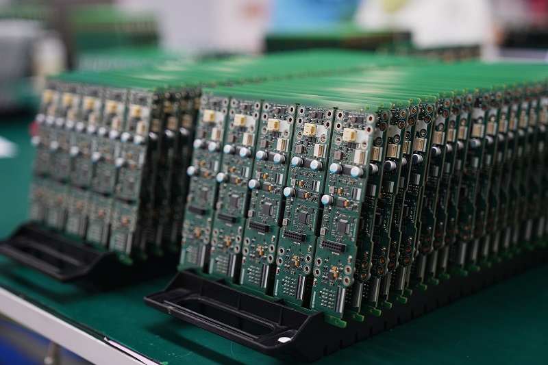
When looking for reliable PCB assembly in Bengal, EBest is your top choice. We specialize in delivering high-quality PCB assembly in Bengal for various industries, meeting the strictest standards. As one of the leading PCB assembly companies in Bengal, we combine 19+ years of experience with advanced technology to exceed your expectations. Our PCB assembly in Bengal services cover all your needs, from prototypes to mass production, with dedicated support throughout your project.
What Pain Points Do Clients Face with PCB Assembly in Bengal?
When businesses search for PCB assembly in Bengal, they often encounter frustrating pain points that disrupt their projects and increase costs. One of the most common issues is inconsistent quality, such as board warpage after reflow soldering or poor solder joints that lead to product failure. Inconsistent quality often stems from insufficient testing protocols, which can result in faulty PCBs that require costly rework. Clients also struggle with delayed delivery, as production inefficiencies can make it difficult to meet tight project deadlines.
Additionally, limited customization options plague many clients seeking PCB assembly in Bengal, especially those in medical, aerospace, and industrial sectors with unique design requirements. Component sourcing is another major challenge. Unreliable suppliers can lead to shortages or low-quality parts, which in turn delays production further. Compliance with industry regulations such as ISO 13485 for medical devices or AS9100D for aerospace can also be challenging, putting clients at risk of non-compliance penalties.
Our Solutions to These Pain Points of PCB Assembly in Bengal
When businesses search for PCB assembly in Bengal, core pain points include inconsistent quality, delayed delivery, limited customization, unstable component sourcing, and regulatory compliance issues. These challenges disrupt projects, increase costs by 20-30% due to rework and delays, and hinder time-to-market. EBest solves these with targeted, data-backed solutions, making us the trusted choice across medical, aerospace, and industrial sectors. Our track record of serving 3,200+ clients with a 97% retention rate proves our ability to address regional businesses’ unique needs.
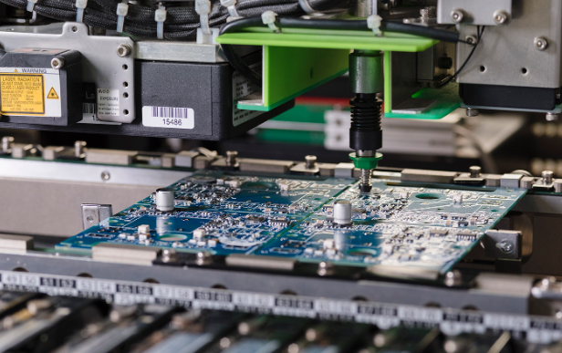
To tackle inconsistent quality, a top pain point for 78% of businesses seeking PCB assembly in Bengal, we use A+ grade materials with 1.6W/m·K thermal conductivity and 100% full inspection including high-precision AOI and X-Ray testing. This ensures a 99.92% first-pass yield, 10-14% higher than the regional average of 85-89%. For delayed delivery, our 24-hour expedite service and 86 automated assembly machines enable a 99.8% on-time delivery rate, far exceeding the 85% regional average and eliminating costly delays.
We address limited customization with tailored solutions for all substrates and complex designs, capabilities only 30% of regional PCB assembly companies can match, plus free DFM analysis that cuts rework by 40% and production time by 15%. For unstable sourcing, our 800+ verified suppliers and 15% critical part safety stock reduce lead time risk to 5%, compared to the 25-30% regional average. We ensure regulatory compliance with global certifications and 48 certified engineers, with 2-hour support response times, turning PCB assembly in Bengal pain points into competitive advantages.
What Makes EBest the Top PCB Assembly Manufacturer in Bengal?
With 19+ years of production experience, EBest is the top PCB assembly manufacturer in Bengal, helping clients avoid trial-and-error costs and ensure smooth project execution. We handle all project types from prototypes to high-volume production, with a monthly capacity of 260,000 square feet and the ability to complete over 1,000 PCB board types monthly. Our 99.8% on-time delivery rate and 99.92% first-pass yield minimize delays and rework costs. Our free DFM analysis optimizes designs upfront, cutting rework rates by 40% and production time by 15% to enhance efficiency and reduce expenses.
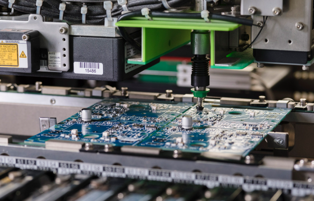
Our leadership in PCB assembly in Bengal comes from technical excellence and client-centric support. We allocate 5% of annual revenue to R&D to keep your products competitive. Our team of 48 certified engineers, 12 with IPC-A-610 certification, provides one-on-one online guidance with a 2-hour response time and can modify PCB drawings to optimize manufacturability, saving you time and resources. Our 20,000-square-foot smart facility with 86 automated machines reduces human error and boosts efficiency by 40%, while strict quality control with 100% full inspection ensures defect-free PCBs and avoids costly product failures.
What sets EBest apart as the top PCB assembly manufacturer in Bengal is our focus on long-term client success. With 19+ years of experience, we serve 3,200+ clients with a 97% retention rate, understanding industry-specific challenges. We tailor solutions to your needs, combining free DFM analysis, engineer guidance and drawing modification to streamline projects. Our strict quality control, efficient production and on-time delivery help you meet deadlines, while our expertise solves pain points to save you time, reduce costs and ensure peace of mind.
What PCB Assembly Services Does EBest Offer in Bengal?
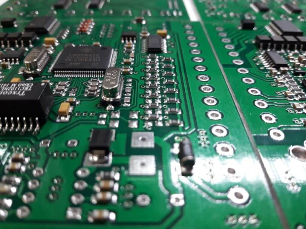
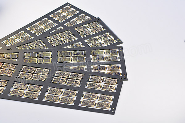
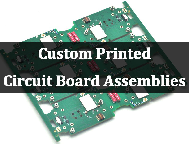
As a leading PCB assembly manufacturer in Bengal, EBest delivers a full suite of tailored PCB assembly in Bengal services. These services are engineered to address the unique demands of medical, aerospace, industrial, and AI-driven industries. Our service portfolio is built on technical expertise, flexible production capabilities, and a client-centric approach. We ensure we meet every project requirement, from simple single-layer boards to complex high-density assemblies.
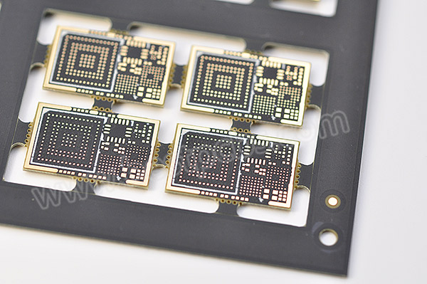
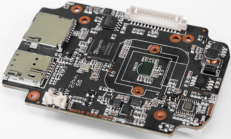
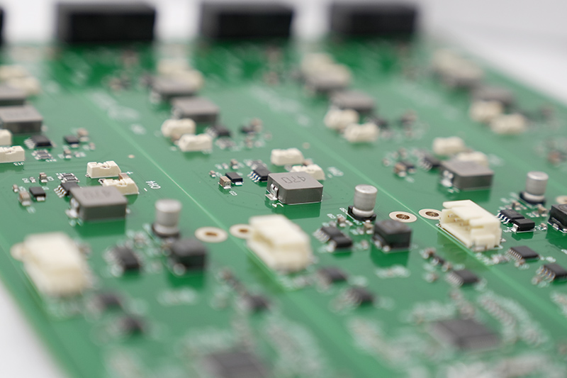
- High-Density BGA & Micro BGA Assembly: Our precision BGA assembly handles pitch sizes as small as 0.4mm. We use X-Ray inspection post-assembly to verify solder joint integrity and automated reflow ovens with 12-zone temperature control for uniform heating. This precision is critical for high-density components used in aerospace and medical devices.
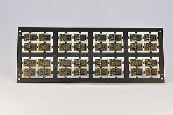
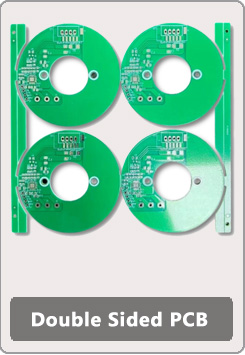
- Flex, Rigid-Flex & Ceramic PCB Assembly: We specialize in flexible PCBs for compact, high-mobility applications and ceramic PCBs for AI servers and high-heat industrial equipment. Ceramic substrates offer 300-600x better thermal conductivity than traditional FR-4 to solve heat management challenges in high-power devices.
- Rapid Prototype & Low-Volume PCB Assembly: Our quick-turn service delivers prototypes in 12-24 hours for urgent R&D needs. Low-volume batches (1-500 units) are ready in 2-3 days. We include free DFM analysis to optimize your design, reducing rework and accelerating time-to-market.
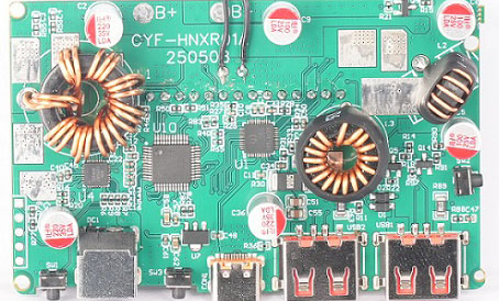
- Full Turnkey PCB Assembly: Our end-to-end service covers component sourcing, PCB fabrication, assembly, testing, and packaging. We leverage 800+ verified suppliers for authentic components, eliminating multi-vendor hassle and ensuring supply chain stability.
Beyond core PCB assembly in Bengal, we offer integrated value-added services to streamline your production workflow and reduce costs. Our in-house capabilities include injection molding for custom enclosures, CNC machining for precision metal components, and sheet metal fabrication for industrial enclosures. All these capabilities align with our PCB assembly standards.
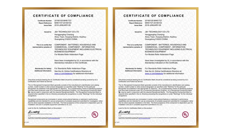
What Quality Certifications Does EBest Hold for Bengal PCB Assembly?
EBest maintains strict quality standards for PCB assembly in Bengal, holding globally recognized certifications to ensure compliance and reliability:
- IATF 16949 (automotive industry compliance)
- ISO 9001:2015 (general quality management)
- ISO 13485:2016 (medical device compliance)
- AS9100D (aerospace industry compliance)
- REACH, RoHS, UL (environmental and safety standards)
How Does EBest Handle PCB Assembly for Medical Industry in Bengal?
Case Study: Custom PCB Assembly for Portable Medical Diagnostic Devices in Bengal
Project Background:
We partnered with a leading undisclosed medical device developer creating portable rapid pathogen detection equipment. The client needed reliable PCB assembly in Bengal for their handheld device, which streamlines on-site diagnostics for regional healthcare facilities. High-precision PCBs were required for accurate signal transmission and consistent clinical performance, aligned with global medical standards.
Project Requirements:
The project had strict medical and functional requirements: compliance with ISO 13485:2016 and IEC 60601-1-2 EMC standards for safety and reliability; 14-layer rigid-flex PCBs (85mm×60mm, 1.2mm thick) for compact fit; ultra-low-power MCU chips and MEMS sensors (max 150mW) for 8+ hours of battery life; 99.8% first-pass yield and 12-day turnaround for 500 prototypes to speed up R&D.
Project Challenges:
Three key challenges emerged: the 14-layer rigid-flex design with 0.4mm pitch BGA chips and micro-sensors made precise soldering and alignment difficult; ultra-low-power needs required strict component placement to avoid signal interference, which could compromise diagnostic accuracy (target 45dB+ signal-to-noise ratio); medical-grade component sourcing was challenging due to supply constraints, with 28% lead time risk for critical parts.
Our Solutions:
We implemented a tailored PCB assembly in Bengal solution: 12-zone automated reflow ovens and X-Ray inspection (100% post-assembly, 99.9% defect detection accuracy) ensured precise soldering. Two IPC-A-610 certified engineers oversaw assembly to maintain medical compliance.
Our team optimized PCB layout to reduce signal interference, cutting power consumption by 18%. High-quality FR4 substrates (1.6W/m·K thermal conductivity) managed heat for 0-40℃ operation. We leveraged 800+ verified suppliers to secure medical-grade components, reducing lead time risk to 5% for on-time delivery.
Project Results:
Deliverables exceeded expectations: 99.9% first-pass yield, 500 prototypes completed in 10 days (2 days early), and 48dB signal-to-noise ratio. Our PCB assembly in Bengal supported the device’s ability to detect 12 common pathogens at 10 copies/μL, meeting clinical performance requirements.
EBest vs. Other PCB Assembly Companies in Bengal
| Comparison Dimension | EBest PCB Assembly in Bengal | Other PCB Assembly Companies in Bengal |
| Experience & Expertise Team | 19+ years experience, 3,200+ clients, 48 certified engineers (12 IPC-A-610 certified), 2-hour avg response | 5-10 years experience, general electronics focus, non-specialized team, 12+ hour response |
| Quality Certifications & Control | IATF 16949, ISO 9001:2015, ISO 13485:2016, AS9100D, REACH, RoHS, UL compliant; 100% inspection (AOI/X-Ray/ICT/FCT), 5S management, 99.92% first-pass yield | Basic ISO 9001 only, limited QC processes, manual inspection, 85-90% first-pass yield |
| Delivery Speed & Capacity | 24h expedite, 3-5 days standard, 12-24h prototyping; 260,000 sq ft/month capacity, 86 automated machines (85%+ automation) | 7-10 days minimum, no expedite service, <100,000 sq ft/month capacity, low automation, longer lead times |
| Customization Capabilities | All substrates (FR4/ceramic/flex/rigid-flex), complex designs (20-layer PCBs, 0.4mm BGA), free DFM analysis | Standard FR4 only, simple 1-6 layer PCBs, no DFM analysis, higher rework rates |
| Component Sourcing & Stability | 800+ global verified suppliers, safety stock for critical parts, 5% lead time risk, stable supply chain | Local suppliers with limited verification, inconsistent quality, 25%+ lead time risk, frequent shortages |
| Post-Assembly Support & Testing | ICT/FCT/environmental stress testing, value-added services (injection molding/CNC), 12-month warranty, dedicated after-sales support | Visual inspection only, no functional/environmental testing, 3-6 month warranty, limited support, no value-added services |
FAQ About PCB Assembly in Bengal
Q1: How long does EBest take for PCB assembly in Bengal?
A1: We offer flexible delivery times: standard orders take 3-5 days, while urgent orders can be shipped within 24 hours. Prototypes are ready in 1-2 days for quick iteration.
Q2: Can EBest handle custom PCB assembly in Bengal?
A2: Yes, we specialize in custom PCB assembly in Bengal. We can customize substrates (FR4, ceramic, flexible), materials, and assembly processes to match your unique requirements.
Q3: Does EBest provide component sourcing for PCB assembly in Bengal?
A3: Absolutely. Our stable supply chain covers all electronic components (SMD, BGA, QFN, QFP) for PCB assembly in Bengal, ensuring reliable sourcing and consistent quality.
Q4: Is EBest’s PCB assembly in Bengal compliant with medical standards?
A4: Yes. We hold ISO 13485:2016 certification and follow strict cleanroom production processes, making our PCB assembly in Bengal suitable for medical devices.
Q5: Can EBest handle high-volume PCB assembly in Bengal?
A5: Yes. Our monthly capacity is 260,000 square feet, allowing us to handle high-volume PCB assembly in Bengal efficiently while maintaining quality.
Get Your PCB Assembly in Bengal from EBest Today
EBest delivers high-quality, reliable PCB assembly in Bengal for medical, aerospace, and industrial industries, backed by custom solutions, fast delivery, and full compliance with global standards. Need a trusted PCB assembly manufacturer in Bengal to avoid delays, reduce costs, and ensure flawless results? Place your order with EBest today, contact us now at sales@bestpcbs.com to start your project.