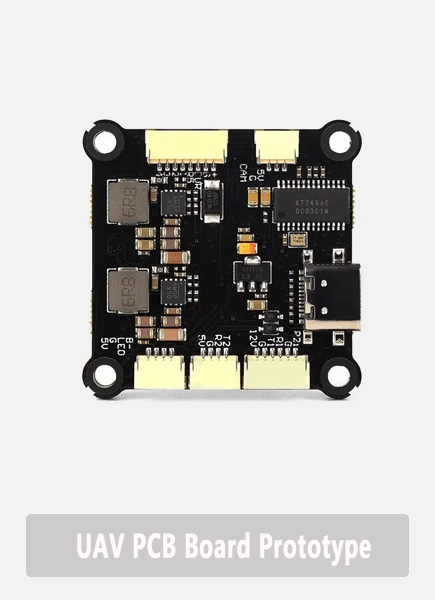
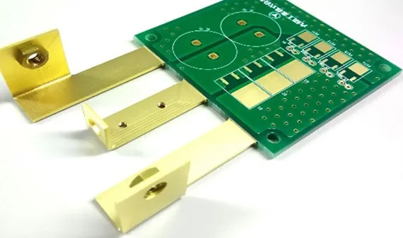
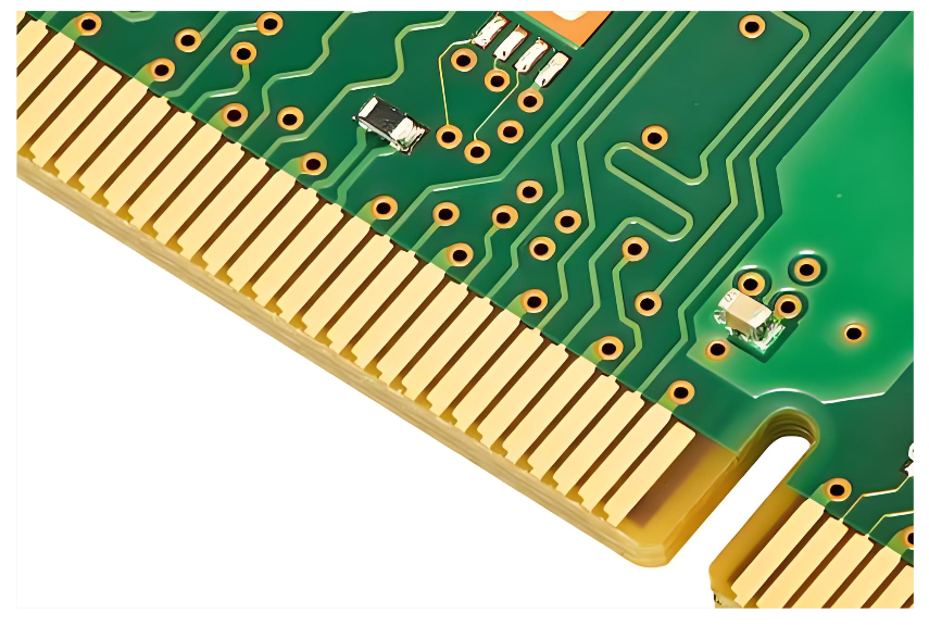
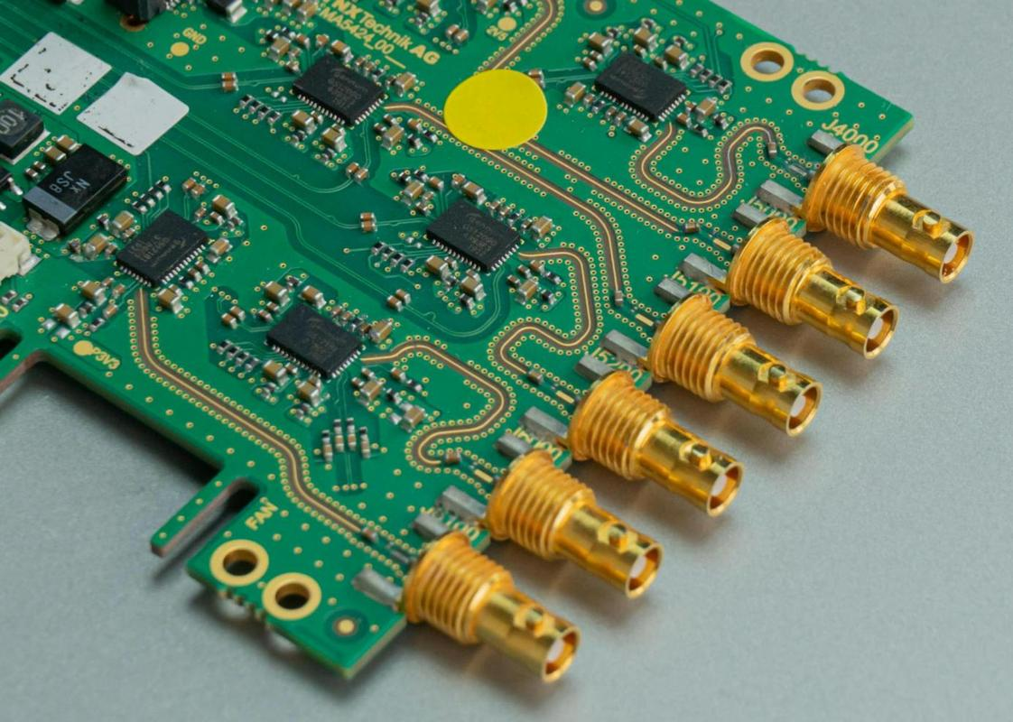
Our PCB on PCB solutions support high-density assembly, reduced size and enhanced functionality for industrial, consumer and automotive electronics.
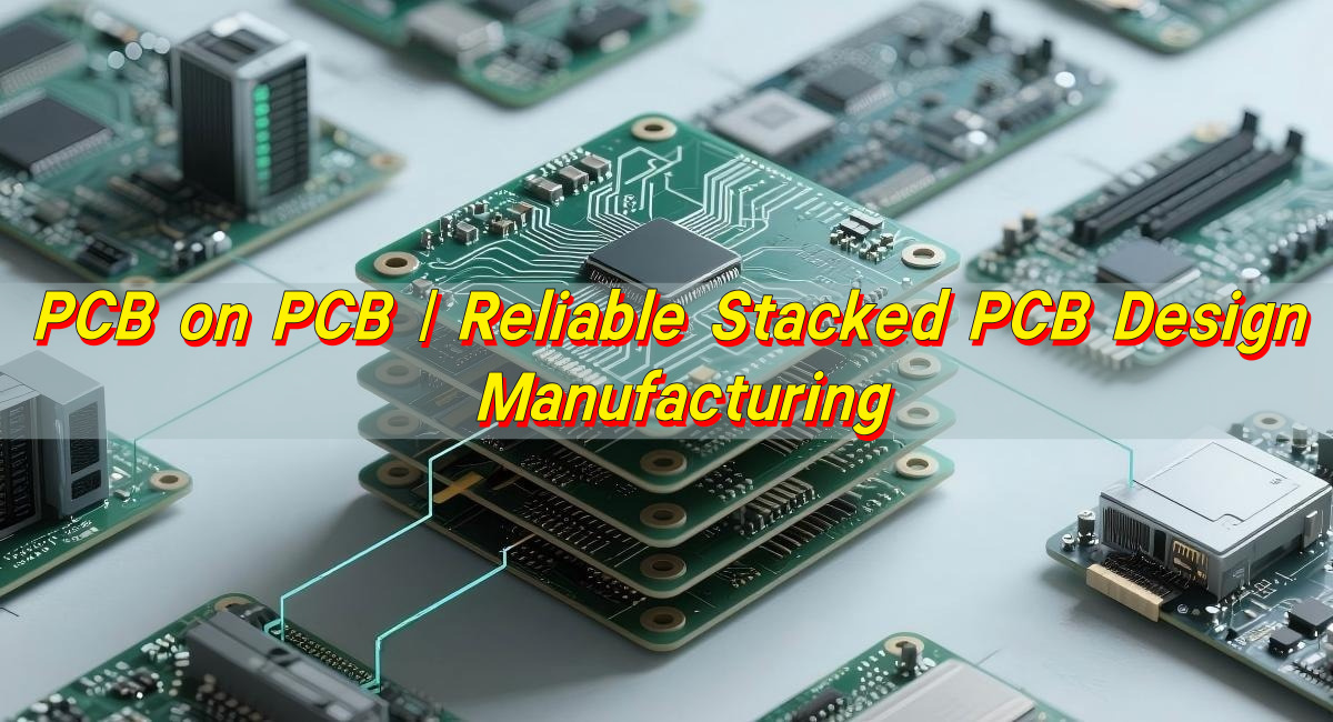
What is PCB on PCB technology?
PCB on PCB technology refers to a design method where one printed circuit board is mounted directly onto another printed circuit board. Instead of placing all electronic circuits on a single board, engineers stack two or more boards together to build a compact and efficient electronic system.
In many modern electronic devices, space is limited. Designers often need to add more features without increasing product size. PCB stacking provides a practical solution. By placing boards vertically, engineers can increase circuit density and integrate more functions in a small area.
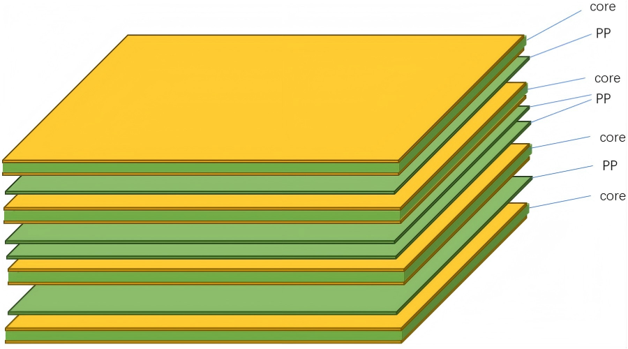
A typical PCB on PCB structure includes a main board and a secondary board. The main board usually handles core functions such as power management, control circuits, and signal routing. The secondary board may include specialized modules like sensors, communication units, or memory components.
Several connection methods are commonly used for stacked boards. These include:
- Board-to-board connectors
- Pin headers
- Mezzanine connectors
- Soldered stacking pins
- Flexible interconnects
Each method serves different design goals. Some offer easy replacement and maintenance, while others provide stronger mechanical stability.
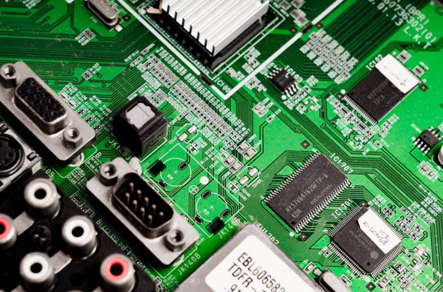
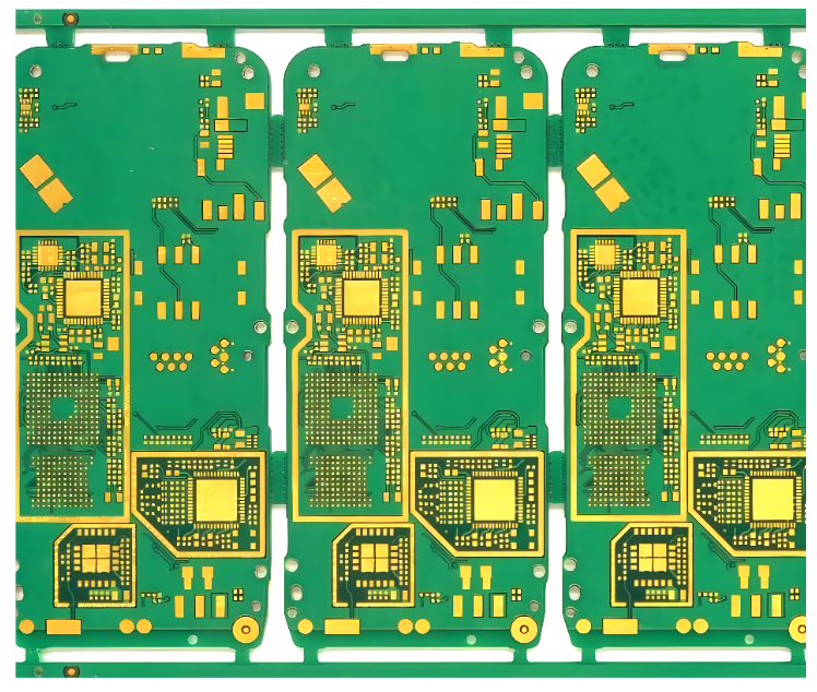
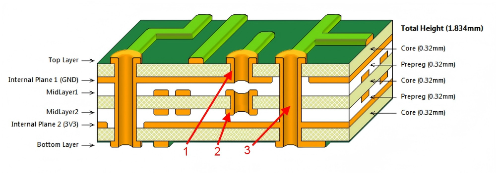
In a PCB on PCB structure, components on a PCB can be distributed across multiple layers. This allows designers to isolate high-frequency circuits, power circuits, and control logic more effectively. It improves signal quality and reduces interference.
Another important aspect of this technology is protective surface treatment. Many stacked boards include coating on PCB surfaces. Conformal coating protects circuits from dust, humidity, and chemical contamination. It is widely used in industrial and automotive electronics. Design engineers also rely on fiducials on PCB surfaces to support automated assembly. Fiducial marks help pick-and-place machines identify accurate component placement positions. When stacking boards, precise alignment becomes even more important.
PCB on PCB technology is widely used in advanced electronics because it provides several clear advantages:
- Higher circuit density
- Compact mechanical design
- Better functional separation
- Flexible module upgrades
Manufacturers such as EBest Circuit (Best Technology) support stacked PCB designs by offering both PCB fabrication and assembly services. With strong engineering support and precise manufacturing processes, stacked board solutions can be implemented efficiently and reliably.
What are the benefits of PCB on PCB stacking?
PCB stacking offers multiple technical and commercial advantages. It helps engineers create powerful electronic systems while keeping device size small and manufacturing costs under control.
One of the most noticeable benefits is space efficiency. Instead of expanding the board horizontally, stacking allows circuits to grow vertically. This approach is especially useful in compact electronics where internal space is limited. Modern electronic devices demand high functionality. PCB stacking allows designers to separate functions across multiple boards. Each board can focus on a specific task such as power control, signal processing, or wireless communication.
Another benefit is improved design flexibility. Engineers can update or replace one board without redesigning the entire system. This modular design method shortens development cycles and simplifies product upgrades.
Key benefits of PCB on PCB structures include:
- Compact electronic design
- Higher circuit density
- Modular architecture
- Easier product upgrades
- Improved signal separation
- Better thermal management
Stacked boards also help manage heat distribution. When circuits are separated across multiple layers, heat can spread more evenly across the structure. This reduces the risk of overheating and improves system reliability. Another advantage is improved signal integrity. Sensitive circuits can be placed on dedicated boards. This reduces electromagnetic interference and improves overall signal performance.
Protective measures such as coating on PCB surfaces also enhance durability. Conformal coatings protect circuits from moisture, vibration, and dust. This makes stacked boards suitable for demanding environments. Fiducials on PCB surfaces also contribute to precise assembly. Automated assembly equipment uses these markers to align components accurately during manufacturing. Accurate alignment becomes essential when multiple boards must connect perfectly.
Manufacturers like EBest Circuit (Best Technology) provide advanced PCB fabrication services that support stacked board applications. Our experience with complex PCB structures ensures reliable electrical performance and long product lifespan.
How does PCB on PCB assembly work?
PCB on PCB assembly involves attaching one circuit board to another while maintaining stable electrical and mechanical connections. The process requires precise manufacturing and careful alignment to ensure long-term reliability.
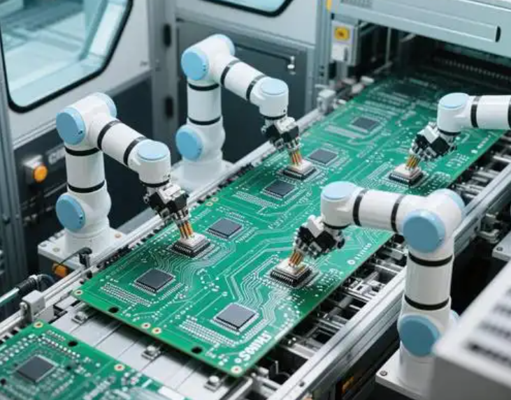
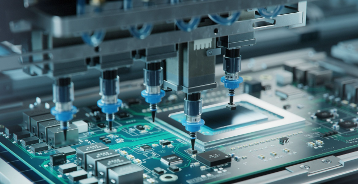
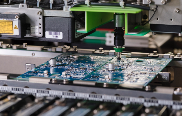
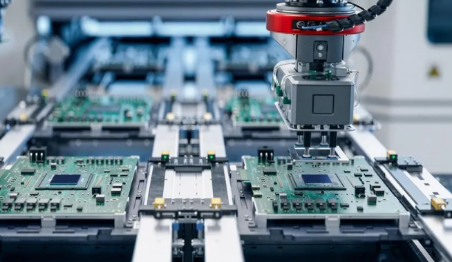
The assembly process usually begins with PCB fabrication. Each board is produced separately according to its design requirements. This includes drilling, copper plating, solder mask application, and surface finishing. Once fabrication is complete, components on a PCB are mounted through standard assembly methods such as surface mount technology (SMT) or through-hole assembly. After individual boards are assembled, the stacking process begins.
The general PCB on PCB assembly workflow includes several steps:
- PCB fabrication
- Component placement and soldering
- Inspection and electrical testing
- Board stacking and connection
- Final functional testing
Different connection methods are used depending on the design. Some stacked boards rely on connectors, while others use soldered pins.
The most common stacking techniques include:
- Board-to-board connectors
- Stacking headers
- Mezzanine connectors
- Direct solder connections
Board-to-board connectors are widely used because they allow easy maintenance and replacement. Mezzanine connectors provide compact spacing and strong electrical performance. During assembly, fiducials on PCB surfaces play a critical role. Automated equipment identifies these reference marks to align boards correctly. Accurate alignment prevents connection failures and ensures consistent assembly quality.
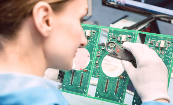
After stacking, the system undergoes multiple inspection steps. These may include:
- Optical inspection
- X-ray inspection
- Electrical testing
- Functional testing
Protective coating on PCB surfaces may also be applied after assembly. This protective layer shields circuits from environmental stress such as moisture or dust.
Reliable PCB assembly requires both precision equipment and experienced engineers. Companies like EBest Circuit (Best Technology) combine automated SMT lines with strict quality control procedures. This ensures that stacked boards meet demanding performance and reliability standards. When properly assembled, PCB on PCB structures provide stable electrical connections and long service life across many electronic applications.
Why use PCB on PCB in electronic design?
Engineers choose PCB stacking because it offers powerful design advantages. As electronic products become smaller and more complex, traditional single-board layouts often reach their limits.
PCB on PCB design allows engineers to break complex circuits into manageable modules. Each board can handle a dedicated function, making the overall system easier to design, test, and maintain. This modular structure improves design efficiency. Teams can develop separate boards simultaneously, reducing development time.
Another major advantage is better signal management. High-frequency circuits, power circuits, and control logic can be placed on separate boards. This physical separation helps reduce signal interference. PCB stacking also improves product scalability. If a new feature is required, engineers can add another board instead of redesigning the entire circuit.
Common reasons engineers adopt PCB stacking include:
- Compact product design
- Functional separation
- Faster development cycles
- Simplified system upgrades
- Improved electrical performance
Components on a PCB can be arranged more efficiently when multiple boards are used. High-density components may be placed on a secondary board while the primary board handles core system functions.
Stacked structures also support specialized protection techniques. For example, coating on PCB surfaces protects circuits from environmental hazards in industrial or outdoor devices. Precision alignment is another key factor. Fiducials on PCB surfaces ensure that automated machines place components accurately during assembly. This is especially important when boards must connect perfectly in stacked designs.
Manufacturers such as EBest Circuit (Best Technology) work closely with engineers during the design phase. Our engineering team helps optimize stacked board structures for performance, reliability, and manufacturability. With the growing demand for compact electronics, PCB stacking continues to play a major role in modern electronic design strategies.
How to test capacitor on PCB?
Testing capacitors directly on a circuit board is an important step during troubleshooting and quality control. Capacitors are widely used for filtering, energy storage, and signal stabilization. A faulty capacitor may cause unstable voltage, signal noise, or system failure. Proper testing helps identify issues before they affect the entire circuit.
The first step in capacitor testing is visual inspection. Engineers check for signs of damage such as:
- Bulging capacitor tops
- Leakage or corrosion
- Burn marks
- Loose solder joints
If physical damage appears, the capacitor should be replaced immediately. Next, electrical testing can be performed using several instruments.
Common testing tools include:
- Digital multimeter
- LCR meter
- Oscilloscope
A digital multimeter can check basic capacitance values and detect short circuits. An LCR meter provides more precise measurements including capacitance, resistance, and inductance. When testing capacitors on stacked boards, access may be limited. Engineers must carefully probe test points without damaging nearby components on a PCB.
In some cases, removing the capacitor from the circuit is necessary to obtain accurate readings. This avoids interference from other circuit elements.
Capacitor testing often follows this general process:
- Power off the device
- Discharge the capacitor safely
- Measure capacitance using a meter
- Compare readings with the rated value
Protective coating on PCB surfaces may slightly complicate testing because probes must contact exposed pads. Engineers should ensure the coating does not prevent reliable measurement. High-quality PCB manufacturing reduces the risk of capacitor failures. Reliable soldering, precise assembly, and careful inspection help ensure long-term circuit stability.
Manufacturers such as EBest Circuit (Best Technology) apply strict quality control during PCB assembly. Our testing procedures help detect potential issues before products reach customers.
How to solder components on PCB?
Soldering components correctly is essential for reliable electronic performance. Poor solder joints can cause intermittent connections, signal loss, or device failure.
Soldering techniques vary depending on the component type and board structure. Surface mount technology is widely used for modern electronics. Components on a PCB are placed directly on solder pads and then soldered using reflow ovens.
Through-hole soldering is another common method. Component leads pass through drilled holes and are soldered on the opposite side of the board.
Basic PCB soldering steps include:
- Clean the PCB surface
- Apply solder paste or flux
- Place components accurately
- Heat the joint using a soldering iron or reflow oven
- Inspect the solder connection
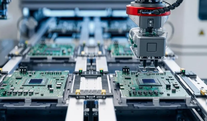
Automated assembly lines often use pick-and-place machines to position components with high precision. Fiducials on PCB surfaces guide these machines during placement. Good solder joints should appear smooth and shiny. They must fully cover the pad and component lead without forming excess solder.
In stacked board designs, soldering becomes more complex because space is limited. Engineers must ensure that solder joints remain accessible for inspection and maintenance. Protective coating on PCB surfaces is usually applied after soldering. This coating protects circuits without interfering with electrical connections.
Professional manufacturers like EBest Circuit (Best Technology) use advanced SMT equipment to ensure consistent solder quality. Automated optical inspection systems detect solder defects early in the production process. Reliable soldering ensures that components remain securely connected throughout the product’s lifetime.
Where is PCB on PCB commonly applied?
PCB stacking is widely used across many industries because it supports compact and high-performance electronics.
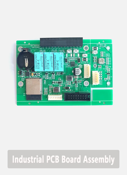
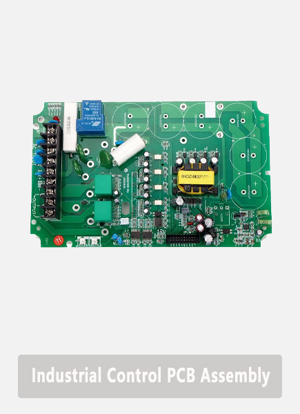
Consumer electronics represent one of the largest application areas. Smartphones, wearable devices, and portable gadgets often rely on stacked boards to maximize functionality in small spaces. Industrial electronics also benefit from PCB stacking. Control systems and automation equipment often require modular designs that support easy maintenance and upgrades.
Common applications include:
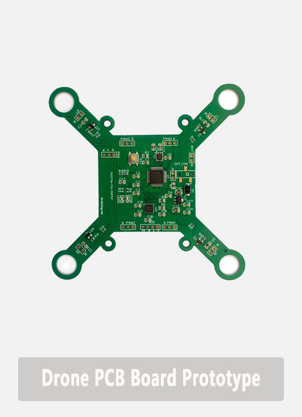
- Smartphones and tablets
- IoT devices
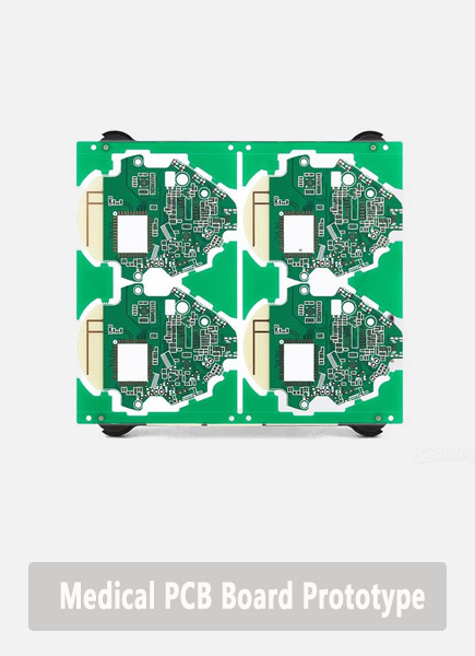
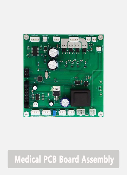
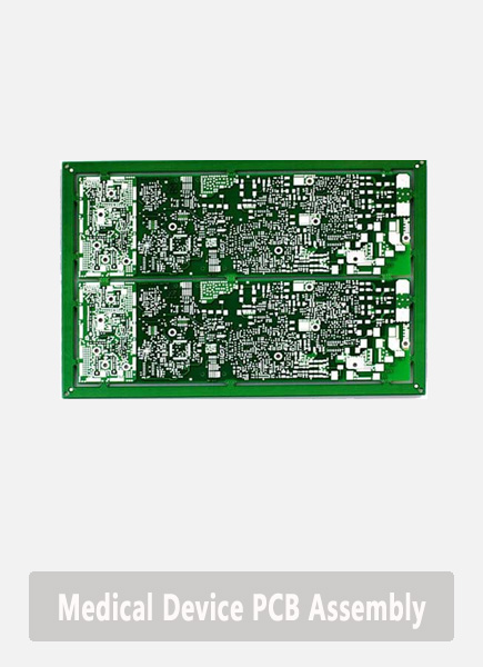
- Medical monitoring equipment
- Automotive electronics
- Communication modules
- Industrial control systems
In medical devices, stacked boards help integrate sensors, processing circuits, and wireless communication modules within compact housings. Automotive electronics also rely on stacked PCB structures. Advanced driver assistance systems and infotainment systems require high circuit density.
Protective coating on PCB surfaces is especially important in these industries because devices often operate in harsh environments. Fiducials on PCB surfaces ensure accurate assembly during high-volume manufacturing. This precision supports consistent product quality across large production runs.
Manufacturers like EBest Circuit (Best Technology) support these industries with reliable PCB fabrication and assembly services. Our experience with complex PCB structures helps customers achieve dependable product performance.
What are the key considerations for PCB on PCB?
Designing a stacked PCB structure requires careful planning. Engineers must consider electrical performance, mechanical stability, and manufacturing feasibility.
One of the most important factors is board spacing. The distance between stacked boards must allow enough room for components while maintaining compact design. Connector selection is also critical. The chosen connector must support the required signal speed, current capacity, and mechanical strength.
Important design considerations include:
- Board spacing and alignment
- Connector reliability
- Signal integrity
- Thermal management
- Mechanical stability
Components on a PCB must be arranged carefully to avoid interference between stacked layers. High-profile components should not block adjacent boards. Thermal management is another key factor. Heat generated by one board should not affect neighboring boards. Engineers may use heat sinks or thermal vias to improve heat dissipation.
Protective coating on PCB surfaces can enhance durability. However, designers must ensure that connectors and test points remain accessible. Fiducials on PCB surfaces are also essential for accurate assembly. Proper placement of these markers ensures reliable alignment during automated production.
Working with an experienced manufacturer greatly simplifies the design process. EBest Circuit (Best Technology) offers engineering guidance to optimize stacked PCB structures and ensure smooth manufacturing.
How to choose PCB on PCB manufacturing services?
Selecting the right manufacturing partner plays a major role in the success of stacked PCB projects. Reliable manufacturers provide both technical expertise and consistent production quality. When evaluating PCB suppliers, engineers should consider several factors including experience, equipment, and quality management systems.
A strong PCB manufacturer typically offers:
- Advanced fabrication capabilities
- Automated SMT assembly lines
- Strict quality control procedures
- Engineering support for design optimization
Experience with stacked board structures is particularly important. PCB on PCB assembly requires precise alignment and reliable connectors. Manufacturers should also provide inspection and testing services to verify electrical performance.
Important evaluation criteria include:
- Production capacity
- Lead time
- Certification standards
- Engineering support
- Quality inspection processes
Protective coating on PCB surfaces and accurate fiducials on PCB placement are also indicators of professional manufacturing standards.
EBest Circuit (Best Technology) has more than 19 years of experience in PCB manufacturing and electronic assembly. The company offers complete services including PCB fabrication, SMT assembly, and stacked board solutions. Our engineering team works closely with customers to ensure each project meets strict reliability requirements. Choosing the right partner ensures that stacked PCB designs are manufactured efficiently and perform reliably throughout the product lifecycle.
Summary:
PCB on PCB technology has become an essential solution for modern electronic design. By stacking multiple circuit boards together, engineers can create compact systems with high functionality and improved performance.
This design approach offers several advantages including higher circuit density, flexible modular architecture, and better signal management. It is widely used in consumer electronics, medical devices, automotive systems, and industrial equipment.
Manufacturers such as EBest Circuit (Best Technology) provide professional support for stacked PCB design and production. With extensive experience in PCB fabrication and assembly, We help engineers transform complex electronic concepts into reliable hardware solutions.
If you are exploring PCB stacking solutions or need professional manufacturing support, feel free to contact: sales@bestpcbs.com