Looking for Top 10 PCB turkey manufacturer? Let’s cover its list, selection guide, service types, evaluation methods of lead time and technical capability for PCB turkey manufacturer.

Why Choose PCB Turkey Manufacturer?
Benefits of PCB Turkey Manufacturer:
Strategic Geographic Location with Low Logistics Costs
- Turkey’s transcontinental position between Europe, the Middle East, and Central Asia enables efficient logistics networks. For European clients, Turkish PCB manufacturers offer “localized supply” solutions, reducing delivery times to 3-5 days and cutting shipping costs by over 50% compared to Far Eastern suppliers.
Significant Cost Efficiency with Outstanding Value
- Labor costs in Turkey are 1/3 to 1/2 of Western European levels, complemented by competitive energy and land expenses. Combined with scalable production capabilities, Turkish PCB quotes typically undercut German or French counterparts by 20-40% while maintaining international quality certifications like ISO 9001 and UL. This achieves an optimal balance of affordability and reliability.
Advanced Technology with Flexible Production Capacity
- Leading Turkish PCB manufacturers have mastered high-end technologies including HDI (High-Density Interconnect), FPCB (Flexible Printed Circuit Boards), and rigid-flex boards. These capabilities support precision requirements for 5G, automotive electronics, and medical devices.
Strict Environmental Compliance and Sustainable Practices
- Turkish factories rigorously adhere to EU environmental regulations such as RoHS and REACH. Most are equipped with advanced wastewater treatment and air purification systems, utilizing lead-free processes and recyclable materials. Many hold ISO 14001 environmental management certifications, meeting global clients’ demands for eco-friendly supply chains.
Integrated Supply Chain for Enhanced Collaboration Efficiency
- Turkey boasts a comprehensive domestic electronics ecosystem encompassing raw material suppliers (copper foil, CCL, plating chemicals) and complementary services like SMT assembly and testing. This “one-stop-shop” capability minimizes cross-regional coordination costs for clients, significantly improving overall project efficiency.
Top 10 PCB Turkey Manufacturer List in 2026
| Company | Main Business | Advantages | Capability | Lead Time |
| EBest Circuit (Best Technology) Co., Ltd | FR4, HDI, MCPCB, ceramic PCB, rigid-flex, SMT | Strong RF/high-speed skills, wide materials, stable quality, full DFM | Multilayer, heavy copper, HDI, flex/rigid-flex | 5–7 days prototype; 2–4 weeks mass |
| Odak PCB | LED PCBs, multilayer, flex, rigid-flex | Strong LED focus, fast service, stable for industrial/auto | LED, single-sided, multi-layer, flex | 5–10 days proto; 3–5 weeks mass |
| Asik Elektronik | PCB + PCBA, flex, aluminum board | One-stop fab + assembly, ISO/UL | FR4, aluminum, flex + SMT/THT | 7–10 days proto; 2–4 weeks PCBA |
| Baski Devre | Single to 32-layer, flex, thick-copper | Long history, good for complex builds | Up to 32 layers, thick copper | 7–12 days proto; 3–5 weeks mass |
| EMS Elektronik | PCB, SMD/THT assembly | Strong automation, good QC | PCB + assembly for auto/medical | 2–3 weeks NPI; 4–6 weeks mass |
| Makro PCB | PCB, SMT/THT, design support | Integrated design + fab + parts | Multi-layer PCBs + EMS | 2–3 weeks proto; 4–6 weeks mass |
| ATEL Teknoloji | Defense electronics, high-reliability cards | Strong R&D, rugged builds | Complex defense PCBs | 6–12+ weeks project-based |
| Net Elektronik | PCB design + fab + assembly | Fast design iterations | Standard + multilayer | 2–3 weeks proto; 3–5 weeks repeat |
| Aktifses Electronics | PCB fab, assembly, reverse-engineering | LED + industrial projects, legacy support | FR4 PCBs + SMT/THT | 2–3 weeks proto; 4–6 weeks mass |
| Bayelektrosan | Single/multilayer PCB + assembly | One of earliest multilayer facilities | Multi-layer + EMS | 2–4 weeks proto; 4–7 weeks mass |
How to Choose the Right PCB Turkey Manufacturer?
Selection Guide to PCB Turkey Manufacturer:
1. Technical Compatibility Data Verification
- Per IPC-6012 standards, qualified manufacturers must support line width/spacing ≤0.1mm (tolerance ±0.02mm), multi-layer boards ≥10 layers with interlayer alignment accuracy ≤75μm. Turkey Electronics Association 2024 report states 75% of local designs require HDI blind/buried via processes. Prioritize manufacturers equipped with LDI exposure machines (accuracy ±5μm) and AOI inspection systems (defect detection rate ≥99.8%).
2. Quality Certification Quantitative Indicators
- ISO 9001 certification requires full-process quality control coverage. UL certification mandates flame retardancy compliance (e.g., FR-4 material achieving 94V-0). Turkey Standards Institution 2023 inspections reveal certified manufacturers maintain defect rates ≤0.3%, significantly lower than non-certified counterparts at 2.1%.
3. Production Cycle Empirical Data
- Standard multi-layer board lead time is 5-7 days (including routine testing), with urgent orders compressible to 3 days. Leading Turkish manufacturers achieve monthly capacity up to 5000 square meters, 85% equipment utilization, and on-time delivery rates ≥98%.
4. Cost-Benefit Comparison Model
- For 10-layer boards, premium pricing includes material costs (40%), processing fees (35%), testing charges (15%), and technical support (10%). Long-term collaboration cases demonstrate selecting manufacturers with DFM design feedback reduces prototype costs by 30%.
5. Localized Support Response Data
- Local technical teams in Turkey provide 24-hour responses to design consultations. Prototype testing cycles reduce to 2 days. Istanbul warehousing centers enable same-day logistics coverage across key regions.
6. Environmental Compliance Standards Data
- Manufacturers complying with RoHS directive must provide hazardous substance test reports (content ≤0.1% for lead, cadmium, etc.). Turkey Ministry of Environment 2024 data shows compliant manufacturers achieve 100% wastewater treatment compliance and ≥85% waste recycling utilization.
7. Customer Case Quantitative Verification
- Well-known Turkish electronics enterprises report delivery quality satisfaction rates of 92% and repeat order rates of 85% with partner manufacturers. Industry forum data indicates premium manufacturers maintain negative review rates ≤3%, well below the industry average of 12%.

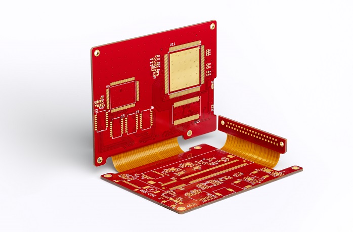
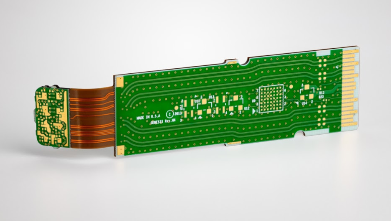
Types of PCB Manufacturing in Turkey
- High-layer rigid PCBs
- High-frequency microwave PCBs
- Rigid-flex PCBs
- HDI (High-Density Interconnect) PCBs with arbitrary layer interconnection
- Aluminum-based PCBs
- Copper-based PCBs
- Thick copper power PCBs
Quality Certification for PCB Manufacturing in Turkey
- CE Mark
- IECQ QC 080000
- ISO 9001:2015
- ISO 14001
- IATF 16949
- ISO 13485
- AS9100D
How to Evaluate the Technical Capability of PCB Manufacturing in Turkey?
Evaluation Guide to Technical Capability of PCB Manufacturing in Turkey:
1. Manufacturing Process Precision Verification
- Verify minimum line width/spacing capabilities (e.g., below 50μm), maximum number of layers (e.g., more than 20 layers), and support for special processes (HDI blind/buried vias, rigid-flex PCBs).
- Sample testing should be conducted according to IPC-A-600 standards, and suppliers are required to provide third-party test reports, such as SGS or TÜV certified data on hole wall copper thickness and impedance control (±10% error range).
2. Equipment and Technology Investment Assessment
- Assess whether the production line is equipped with laser drilling machines (e.g., capable of drilling holes smaller than 50μm), automatic optical inspection (AOI) equipment, and flying probe testers.
- Confirm the adoption of Industry 4.0 intelligent systems, such as MES (Manufacturing Execution System) for real-time monitoring of yield rate (target ≥98%) and AOI inspection coverage (≥95%).
3. Quality Certification and Standard Compliance
- Verify certifications such as ISO 9001, TS 16949, and UL certification, ensuring compliance with international standards such as IPC-6012, RoHS, and REACH.
- Verify whether the supplier has experience in producing automotive-grade PCBs (AEC-Q200) or medical-grade PCBs (ISO 13485), and request historical project case data.
4. Material Supply Chain Transparency
- Evaluate the source of base materials (e.g., mainstream brands such as Isola and Ventec), copper foil type (e.g., HVLP low-loss copper foil), and surface treatment processes (ENIG, OSP).
- Require suppliers to disclose their raw material supplier list and verify their ISO 14001 environmental certification to ensure supply chain stability.
5. R&D and Innovation Capabilities
- Assess whether the company has an independent R&D team and patented technologies (e.g., high-frequency/high-speed material applications, micro-via filling processes).
- Evaluate their ability to support complex designs, such as development cases and test data for RF PCBs (5G frequency band) and high-heat dissipation substrates (metal-based/ceramic-based) (e.g., thermal conductivity ≥2.0W/mK).

How to Evaluate the Lead Time of PCB Manufacturing in Turkey?
Evaluation Guide to Lead Time of PCB Manufacturing in Turkey:
- Clarify demand stage division by breaking lead time into six core phases: order confirmation, engineering evaluation, material procurement, production manufacturing, quality inspection, and logistics. Demand suppliers provide standard duration and fluctuation range for each phase to avoid vague commitments.
- Verify local supply chain by prioritizing manufacturers with local warehouses or partner material suppliers in Turkey. Ensure critical materials like substrates and solder masks are allocated within 24 hours to avoid 15-30 day delays from international sea freight.
- Evaluate engineering capabilities by requiring suppliers to share engineering modification counts and average processing times for similar PCB orders in the past three months. For complex designs like HDI or high-frequency boards, confirm engineer qualifications and CAM software compatibility.
- Ensure production scheduling transparency by demanding suppliers provide real-time production dashboards or ERP system screenshots. Confirm current capacity utilization rates and your order’s position in the production queue to prevent delays from insufficient capacity.
- Standardize quality inspection by defining clear criteria such as IPC-A-600G Class 2/3. Require suppliers provide recent external audit reports and defective product handling cases to ensure inspection time is controlled (typically 1-3 days).
- Compare logistics options by analyzing air freight (3-5 days), land transport (7-10 days), and sea freight (20-30 days) timeliness and costs. Demand suppliers demonstrate last-mile delivery coverage in Turkey and door-to-door solutions for urgent orders.
- Validate historical data by requiring suppliers share actual delivery time statistics for similar orders in the past six months. Focus on verifying the deviation rate between promised and actual delivery times (should be within ±5%).
- Develop risk contingency plans for Turkish holidays (e.g., Eid al-Fitr, Republic Day) and peak logistics seasons (e.g., Black Friday, Christmas). Require suppliers provide emergency plans like backup production lines and multimodal transport to ensure delivery stability during special periods.
Frequently Asked Questions About PCB Manufacturing in Turkey
Q1: What causes price variations in Turkish PCBs?
A1: Price differences stem from material selection, capacity constraints, surface finish options, and QC intensity. Standardizing material sourcing (e.g., Rogers, Isola) and optimizing panel utilization stabilizes pricing, with transparent cost breakdowns for material, plating, and testing charges.
Q2: Can Turkish manufacturers produce HDI, RF, microwave or ceramic PCBs?
A2: Most factories focus on basic FR4, while few support high-complexity products. Available options include HDI (1+n+1/2+n+2 structures), PTFE RF boards (RO4350B/RO3003), AlN/Al₂O₃ ceramic substrates, and precision impedance-controlled multilayers with strict tolerance control.
Q3: What are typical PCB lead times in Turkey and how to avoid delays?
A3: Standard lead times for multilayer/flex/LED boards range 2-5 weeks. Delays often result from engineering rechecks, unclear stack-ups, or material shortages. Solutions include early DFM validation, rapid stack-up confirmation, locked production schedules, and 5-7 day express builds for urgent needs.
Q4: How reliable is quality control among Turkish PCB suppliers?
A4: Some plants lack full-process AOI, flying probe, or impedance analysis, affecting consistency for high-frequency/high-density boards. Full-process QA includes step-by-step AOI, 100% electrical testing, impedance verification, microsection reports, solderability testing, and MES traceability, with COC and material certificates provided per shipment.
Q5: Can local Turkish EMS handle complex component sourcing for PCBA?
A5: Local EMS often struggle with RF components, BGAs, fine-pitch ICs, and long-lead parts due to limited inventory. Global sourcing channels (China/Vietnam) secure hard-to-find components, supporting turnkey PCB+SMT assembly with SPI/AOI/X-Ray inspection, process tuning, and sample validation to reduce procurement risk and improve yield.