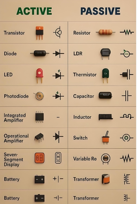
Why Choose EBest as Your Preferred PCB Manufacturer in Israel
When sourcing a PCB manufacturer in Israel, EBest stands out with proven performance across critical metrics. We deliver consistent on-time delivery, zero-defect quality, full regulatory compliance, and flexible support for every project stage.
- On-Time Delivery: 99% on-time rate for prototypes and mass production, with expedited options for urgent Israeli projects
- Uncompromising Quality: Full in-house testing (AOI, X-ray, impedance verification) to meet IPC Class 2/3 standards
- Global Certifications: ISO 9001, AS9100, ISO 13485, and IATF 16949 for medical, automotive, and aerospace applications
- Cost-Effective Support: Free DFM analysis, low or no MOQ for prototypes, and transparent pricing without hidden fees
- Dedicated Local Support: An English-speaking engineering team for real-time design collaboration and issue resolution

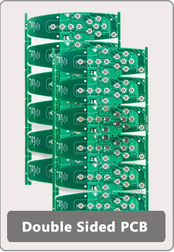
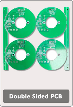
PCB Manufacturer in Israel

Comprehensive PCB Manufacturing & Assembly Services by EBest
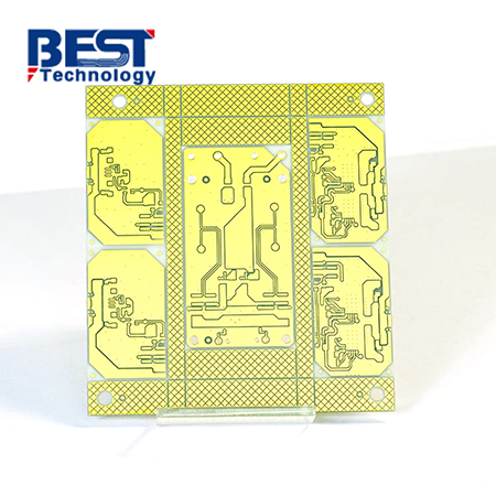
EBest provides end-to-end PCB manufacturing in Israel for all volume and complexity needs, from quick-turn prototypes to full-scale mass production.
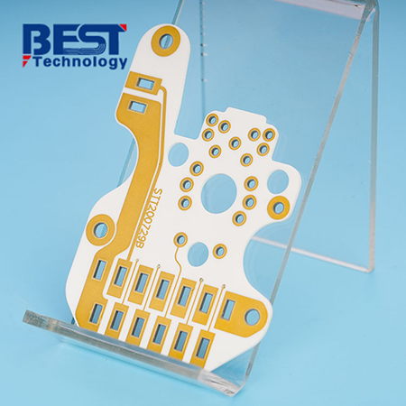
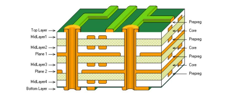
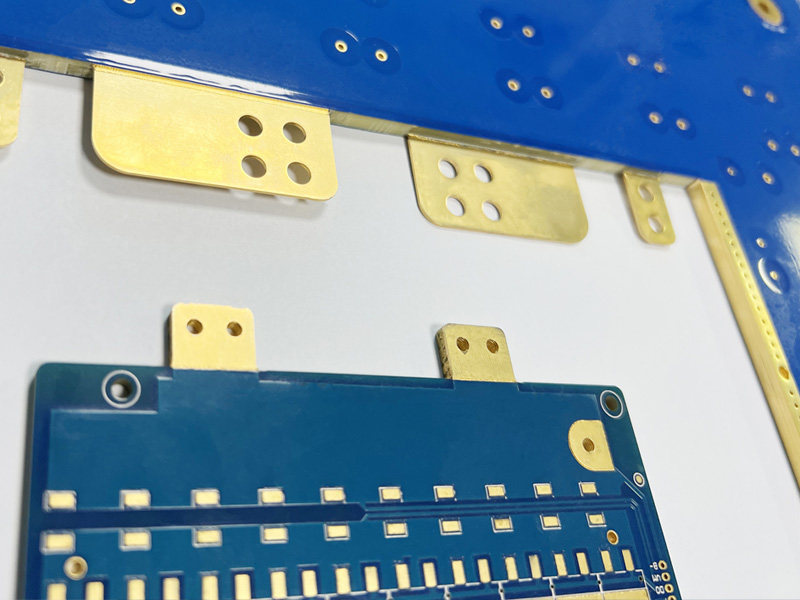
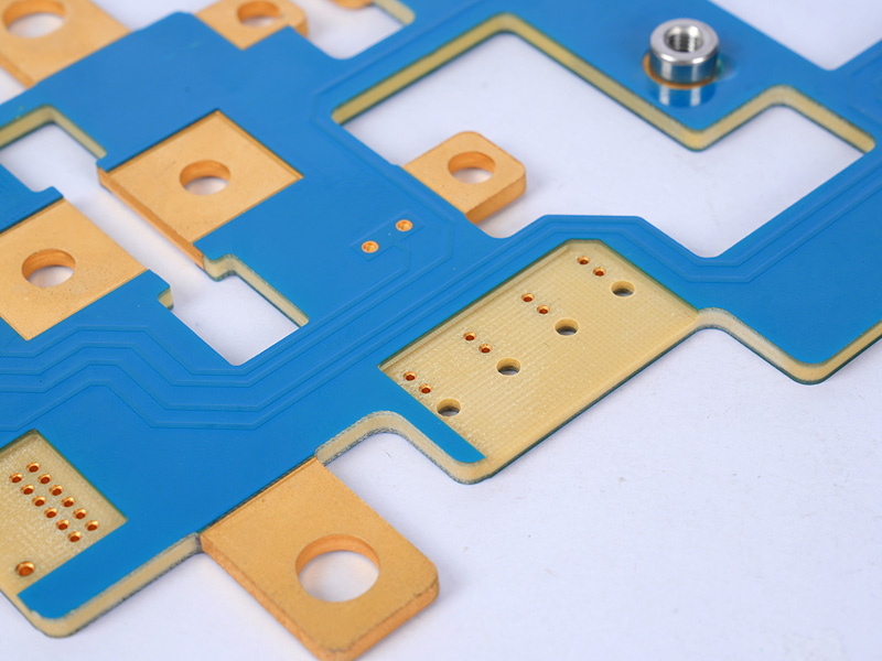
- Rigid, flex, rigid-flex, HDI, RF/high-frequency, ceramic, thick-copper, and micro-via PCB fabrication
- Full PCBA assembly: SMT, through-hole, BGA, micro-BGA, and mixed-technology assembly
- Scaling from prototype to mass production with consistent process control
- Custom stack-up, surface finish (ENIG, immersion silver, HASL), and material selection (FR-4, Rogers, ceramic, polyimide)
- Free DFM report with every order to optimize design for manufacturability and reduce rework
- On-demand customization for specialized Israeli high-tech applications
EBest’s Industry Certifications & Quality Accreditations
Our certifications validate compliance with global and Israeli industry standards, ensuring your PCB manufacturer in Israel meets strict regulatory requirements.
- ISO 9001:2015 – Quality management system
- AS9100D – Aerospace & defense quality standard
- ISO 13485 – Medical device manufacturing compliance
- IATF 16949 – Automotive electronics quality management
- IPC-A-610 Class 2/3 – PCB assembly acceptability standards
- RoHS & REACH compliant – Environmental material restrictions
- ITAR registered – For defense and aerospace projects requiring U.S. compliance
Key Challenges in Israeli PCB Sourcing & How EBest Solves Them
Israeli electronics teams face unique hurdles when sourcing PCBs locally—long lead times, limited advanced capabilities, high prototype costs, and inconsistent DFM support. EBest eliminates these pain points with targeted solutions.
We cut prototype lead times by 50% compared to local Israeli suppliers with our quick-turn fabrication lines. Our advanced in-house equipment supports HDI, ceramic, and RF PCBs that many local manufacturers cannot produce. We provide free DFM analysis upfront to catch design flaws before production, reducing costly rework cycles.
Our flexible MOQ policy lets you order small prototype runs without premium pricing. For Israeli projects, we offer dedicated engineering support in English to align with local design teams and ensure seamless communication. Choose EBest as your PCB manufacturer in Israel for reliable, cost-effective, and technologically advanced PCB solutions.
Top 10 PCB Manufacturers in Israel: Verified List with Certifications & Services
| Manufacturer Name | Certifications | Primary Products & Services | Key Industries |
|---|---|---|---|
| Nistec (Eltek) | AS9100, ISO 9001, ISO 13485, IATF 16949 | Rigid/flex PCBs, HDI, assembly, aerospace/medical | Aerospace, Medical, Automotive, Defense |
| PCB Technologies | ISO 9001, AS9100, Nadcap | Multilayer rigid, rigid-flex, prototype to mass production | Telecom, Aerospace, Industrial |
| IDANics L.T.D | ISO 9001 | 28-layer rigid, ceramic/FR-4, automotive/medical | Automotive, Medical, Industrial |
| Flexitech Avia | ISO 9001 | Flexible/rigid PCBs, aluminum/ceramic substrates | Lighting, Industrial, Consumer |
| Newline-PCB | N/A | Rigid-flex, polyimide/Kapton, 14-layer designs | Aerospace, Medical, Telecom |
| Ma’agalim D.S. Ltd | ISO 9001 | HDI, flex, rigid PCBs, microvias | Telecom, Industrial, Consumer |
| Elcad PCB Ltd | UL, ISO 9001 | 28-layer rigid, aerospace-grade, copper core | Aerospace, Defense, Medical |
| PCB Runner | ISO 9001 | Quick-turn prototypes, rigid/flex, RF PCBs | R&D, Industrial, Telecom |
| P.C.L Electronics Ltd | N/A | Rigid/flex, 20-layer, aluminum substrates | Industrial, Lighting, Consumer |
| Inviatech PCB Engineering | ISO 9001 | Design, layout, prototype fabrication, DFM support | R&D, Startups, Industrial |
DFM Guidelines & Local Manufacturing Constraints for Israeli PCB Production
Israeli PCB facilities have specific process limits that impact design feasibility—understanding these rules prevents costly delays and redesigns.
Local manufacturers typically support up to 28 layers for rigid PCBs, with limited HDI/microvia capabilities compared to global suppliers. Minimum line width/space is often 4/4 mil for standard production, with tighter tolerances requiring premium pricing.
Material selection is restricted to FR-4, standard Rogers, and basic ceramic; high-frequency RF or specialized ceramic substrates may require import. Via-in-pad and stacked microvias are not widely available locally.
EBest provides free DFM analysis tailored to Israeli manufacturing constraints, optimizing your design to balance performance, cost, and local production feasibility.
Lead Time, MOQ & Production Volume Comparison: Prototype vs Mass Production
Balancing speed, quantity, and cost is critical for Israeli projects—here’s how prototype and mass production compare for PCB manufacturer in Israel options.
| Production Stage | Typical Lead Time (Local Israel) | Typical Lead Time (EBest) | MOQ Requirement |
|---|---|---|---|
| Quick-Turn Prototype | 7–14 days | 3–5 days | 1–5 pcs (No MOQ) |
| Standard Prototype | 10–20 days | 5–7 days | 5–10 pcs |
| Low-Volume Production | 20–30 days | 10–15 days | 50–100 pcs |
| Mass Production | 30–45 days | 15–25 days | 500+ pcs |
EBest delivers faster lead times across all volumes while maintaining the same high-quality standards as local Israeli manufacturers.
How to Select a Reliable PCB Manufacturer in Israel: Avoid Common Pitfalls
Choosing the right PCB manufacturer in Israel requires evaluating technical capability, quality, compliance, and support—avoid these costly mistakes.
- Skip verifying certifications: Always confirm ISO, AS9100, or industry-specific accreditations for your application.
- Ignore DFM support: Lack of upfront design review leads to 30%+ rework costs and delays.
- Underestimate advanced capability needs: Many local firms cannot handle HDI, RF, or ceramic PCBs.
- Overlook communication barriers: Ensure English-speaking engineering support for seamless collaboration.
- Neglect scalability testing: Confirm the manufacturer can scale from prototype to mass production without quality drops.
EBest eliminates all these risks with full transparency, advanced capabilities, and dedicated support.
Advanced PCB Capabilities in Israel: HDI, RF, Ceramic, Rigid-Flex & High-Reliability Solutions
Israeli high-tech sectors demand advanced PCBs—here’s what’s available locally and how EBest fills capability gaps.
Local Israeli manufacturers excel at standard rigid PCBs but lack consistent capacity for HDI (microvias, 9+N+9 structures), high-frequency RF (Rogers/Taconic), ceramic substrates, and complex rigid-flex designs. These technologies are critical for Israeli aerospace, medical, and telecom projects.
EBest specializes in these advanced processes:
- HDI PCBs with 2/2 mil line width, microvias down to 3 mil, and via-in-pad
- RF/high-frequency PCBs with impedance control ±5% and low-loss materials
- Ceramic PCBs for high-temperature, high-thermal-conductivity applications
- Rigid-flex PCBs with up to 20 layers for space-constrained designs
DFM & Engineering Support: Reduce Rework & Boost Yield for Israeli Projects
DFM (Design for Manufacturability) is the single biggest factor in reducing production issues and costs for PCB manufacturer in Israel projects.
Israeli design teams often face misalignment between design intent and local manufacturing capabilities, leading to repeated redesigns and missed deadlines. EBest provides complimentary, expert DFM analysis with every order:
- Review layer stack-up, trace width/spacing, via size, and clearances for local process compatibility
- Identify and resolve manufacturability issues before production starts
- Optimize panel utilization to reduce material waste and cost
- Provide clear design recommendations in English, aligned with Israeli project requirements
This support cuts rework by up to 40% and improves first-pass yield to 98%+.
Industry Case Studies: EBest PCB Solutions for Israeli High-Tech Sectors
EBest has delivered custom PCB manufacturing in Israel solutions for four high-demand Israeli industries, solving critical technical challenges.
Aerospace & Defense
We produced 16-layer rigid-flex HDI PCBs for Israeli drone navigation systems, with microvias and impedance control for reliable signal transmission in high-vibration environments. The design met AS9100 standards and reduced weight by 30% compared to traditional rigid boards.
Medical Devices
ISO 13485-certified ceramic PCBs for portable Israeli diagnostic equipment provide excellent thermal stability and biocompatibility. The boards supported high-density component placement and passed rigorous medical regulatory testing.
Industrial Automation
Thick-copper (4oz) PCBs for Israeli industrial control systems handle high current loads and extreme temperature fluctuations. The design included heavy copper planes for heat dissipation and improved long-term reliability.
Telecom Infrastructure
RF/high-frequency PCBs using Rogers materials for Israeli 5G base station components feature precise impedance control and low signal loss. The boards supported high-speed data transmission and met strict telecom performance standards.
FAQ: Common Questions About PCB Manufacturing in Israel
What certifications should I look for in a PCB manufacturer in Israel?
Prioritize ISO 9001 (quality), AS9100 (aerospace), ISO 13485 (medical), and IATF 16949 (automotive) based on your industry. RoHS/REACH compliance is also essential for global distribution.
How long does PCB prototyping take in Israel?
Local prototype lead times range from 7–14 days; EBest delivers in 3–5 days with expedited options for urgent Israeli R&D projects.
Can Israeli PCB manufacturers produce HDI or ceramic PCBs?
Most local firms have limited HDI/ceramic capabilities. EBest specializes in these advanced processes for Israeli projects requiring high-performance PCBs.
What is the typical MOQ for PCB prototypes in Israel?
Local manufacturers often require 10+ pcs; EBest offers no MOQ for prototypes to support Israeli startups and R&D teams.
Do Israeli PCB manufacturers provide DFM support?
Many offer basic DFM, but few provide detailed, English-language analysis. EBest includes free comprehensive DFM reports with every order.
Can I get custom PCB materials in Israel?
Standard FR-4 is readily available; specialized materials (Rogers, ceramic) often require import. EBest sources and fabricates with all high-performance materials for Israeli clients.
How does EBest ensure quality for Israeli PCB orders?
We perform 100% AOI, X-ray inspection, impedance testing, and functional verification, with full traceability and compliance with IPC Class 2/3 standards.
Final Call to Action
EBest provides custom PCB manufacturing in Israel with free DFM reports and full technical support for every project. For high-quality, on-time PCB solutions tailored to Israeli high-tech needs, contact us at sales@bestpcbs.com to start your order.